
FPGA based implementation of divider in Finite field
FPGA based implementation of divider in Finite field Final MS Project by Fareena Fiaz Advisor Dr Shahid Masud Lahore University of Management Sciences (LUMS) 5 th July 2004
Overview ¡ Problem description l l l ¡ ¡ Related work My contribution l l l ¡ ¡ ¡ Finite field Representing Alpha values Finite/Galois field algebra Division algorithms Efficient hardware requirements Project phases Design flow UMD Algorithm, pseudocode, description, state diagram C code implementation Verilog code results & timing diagram Implementation, synthesis for a FPGA (Field Programmable Gate Array) Conclusion Future work References 2
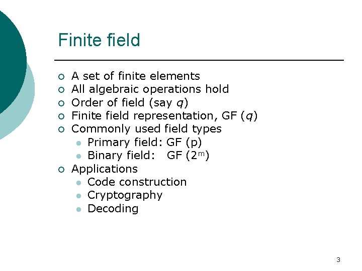
Finite field ¡ ¡ ¡ A set of finite elements All algebraic operations hold Order of field (say q) Finite field representation, GF (q) Commonly used field types l Primary field: GF (p) l Binary field: GF (2 m) Applications l Code construction l Cryptography l Decoding 3
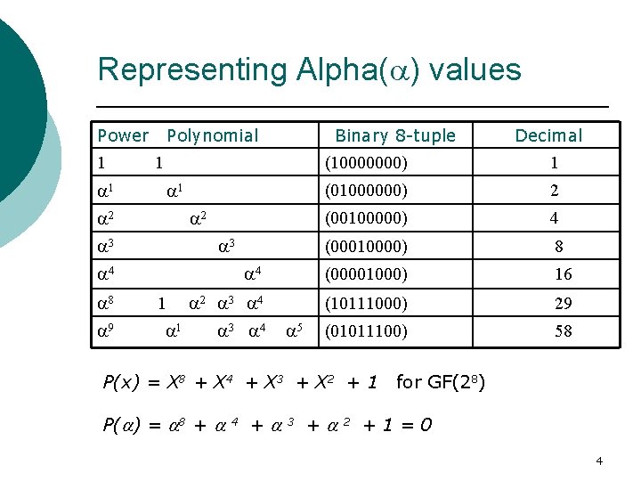
Representing Alpha( ) values Power Polynomial Binary 8 -tuple Decimal 1 1 (10000000) 1 1 (01000000) 2 2 2 (00100000) 4 3 3 (00010000) 8 4 4 (00001000) 16 8 1 2 3 4 (10111000) 29 9 1 3 4 5 (01011100) 58 P(x) = X 8 + X 4 + X 3 + X 2 + 1 for GF(28) P( ) = 8 + 4 + 3 + 2 +1=0 4

Finite/Galois field algebra ¡ ¡ ¡ Field – a number system with defined fundamental operations (+, -, /, x) Galois Field (GF) is a finite field GF(2 m ) m=8 Multiplication: i * j = [(i + j) mod (2^m - 1)] Division: i / j = [(i - j) mod (2^m - 1)] l Example: 5 * 4 = 9 mod 7 = 2 Addition/Subtraction: ( use binary XOR) l Example: (00011001) + (10110100) = (10101101) 5
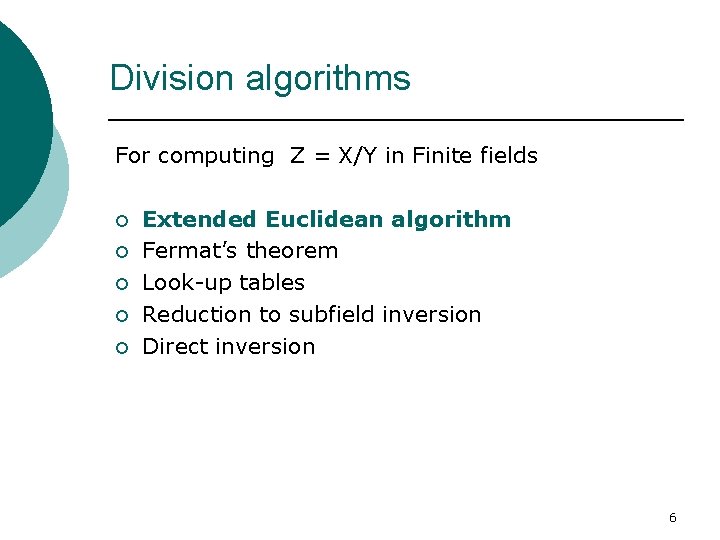
Division algorithms For computing Z = X/Y in Finite fields ¡ ¡ ¡ Extended Euclidean algorithm Fermat’s theorem Look-up tables Reduction to subfield inversion Direct inversion 6
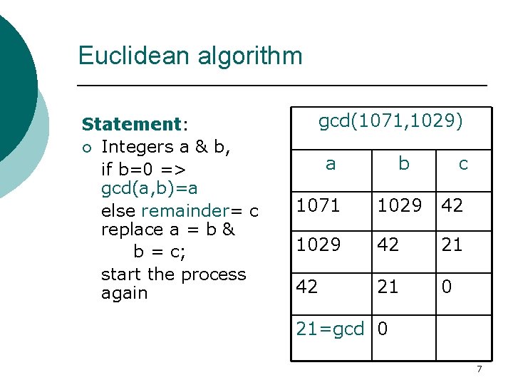
Euclidean algorithm Statement: ¡ Integers a & b, if b=0 => gcd(a, b)=a else remainder= c replace a = b & b = c; start the process again gcd(1071, 1029) a b c 1071 1029 42 21 0 21=gcd 0 7
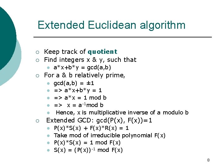
Extended Euclidean algorithm ¡ ¡ Keep track of quotient Find integers x & y, such that l ¡ For a & b relatively prime, l l l ¡ a*x+b*y = gcd(a, b) = ± 1 => a*x+b*y = 1 => a*x = 1 mod b => x = a-1 mod b Hence, x is multiplicative inverse of a modulo b Extended GCD: gcd(P(x), F(x))=1 l l P(x)*S(x) + F(x)*R(x) = 1 Take mod of irreducible polynomial F(x) P(x)*S(x) = 1 mod F(x) S(x) = (P(x))-1 mod F(x) 8
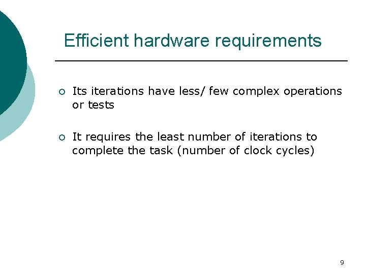
Efficient hardware requirements ¡ Its iterations have less/ few complex operations or tests ¡ It requires the least number of iterations to complete the task (number of clock cycles) 9
Overview ¡ Problem description l l l ¡ ¡ Related work My contribution l l l ¡ ¡ ¡ Finite field Representing Alpha values Finite/Galois field algebra Division algorithms Efficient hardware requirements Project phases Design flow UMD Algorithm, pseudocode, description, state diagram C code implementation Verilog code results & timing diagram Implementation, synthesis for a FPGA (Field Programmable Gate Array) Conclusion Future work References 10

Systolic VLSI implementation [2][3] ¡ Serial-in serial-out architectures ¡ Parallel-in serial-out architectures ¡ Serial-in parallel-out architectures 11
Overview ¡ Problem description l l l ¡ ¡ Related work My contribution l l l ¡ ¡ ¡ Finite field Representing Alpha values Finite/Galois field algebra Division algorithms Efficient hardware requirements Project phases Design flow UMD Algorithm, pseudocode, description, state diagram C code implementation Verilog code results & timing diagram Implementation, synthesis for a FPGA (Field Programmable Gate Array) Conclusion Future work References 12
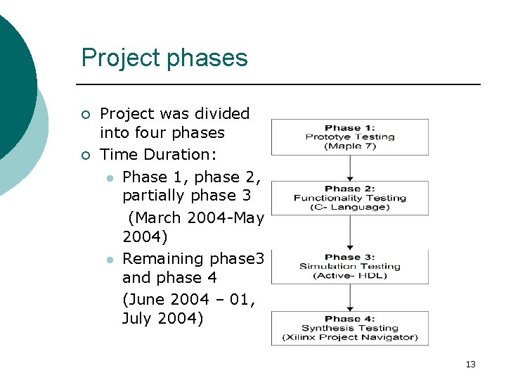
Project phases ¡ ¡ Project was divided into four phases Time Duration: l Phase 1, phase 2, partially phase 3 (March 2004 -May 2004) l Remaining phase 3 and phase 4 (June 2004 – 01, July 2004) 13
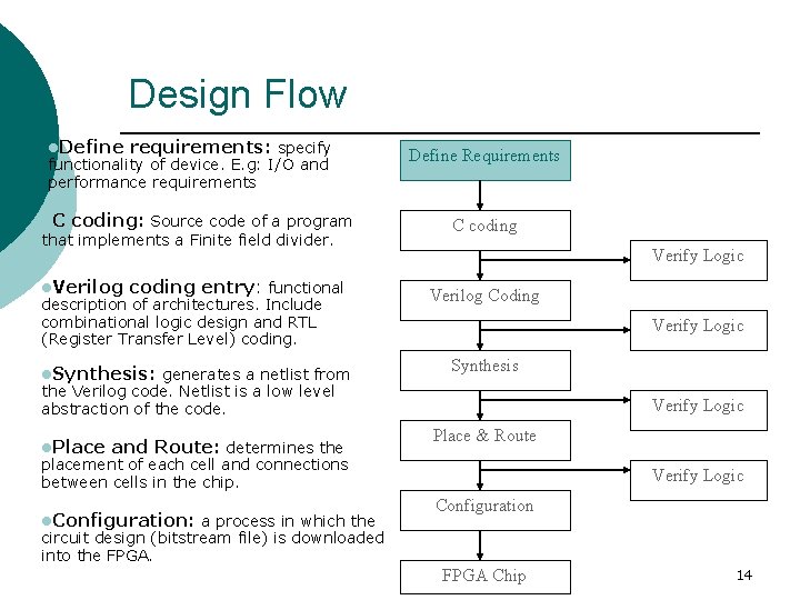
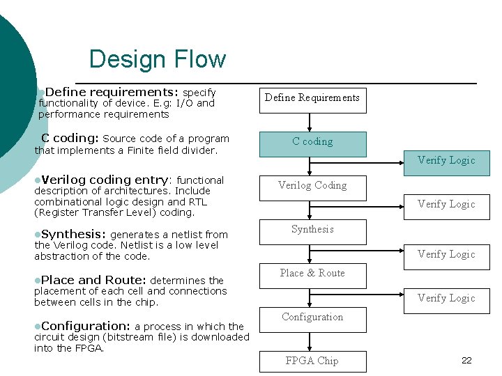
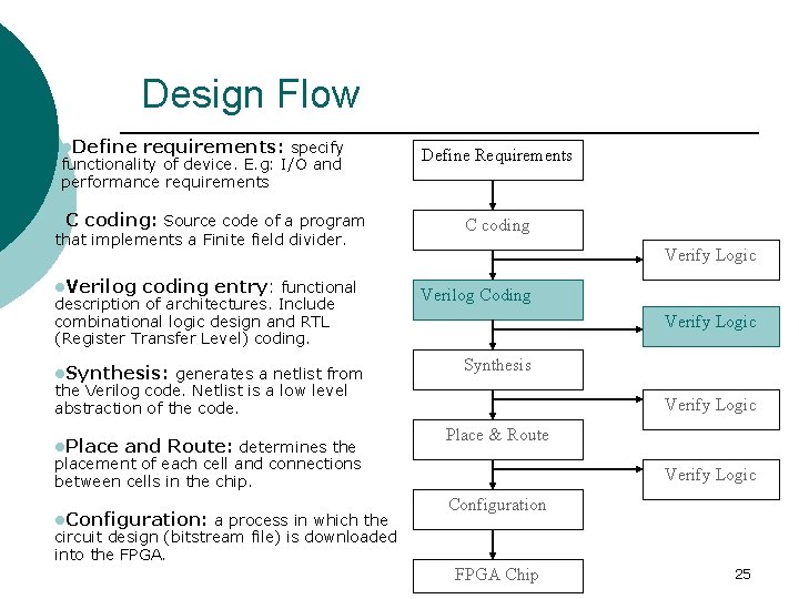
Design Flow l. Define requirements: specify functionality of device. E. g: I/O and performance requirements l. C coding: Source code of a program that implements a Finite field divider. l. Verilog coding entry: functional description of architectures. Include combinational logic design and RTL (Register Transfer Level) coding. l. Synthesis: generates a netlist from Define Requirements C coding Verify Logic Verilog Coding Verify Logic Synthesis the Verilog code. Netlist is a low level abstraction of the code. l. Place and Route: determines the Verify Logic Place & Route placement of each cell and connections between cells in the chip. l. Configuration: a process in which the circuit design (bitstream file) is downloaded into the FPGA. Verify Logic Configuration FPGA Chip 14
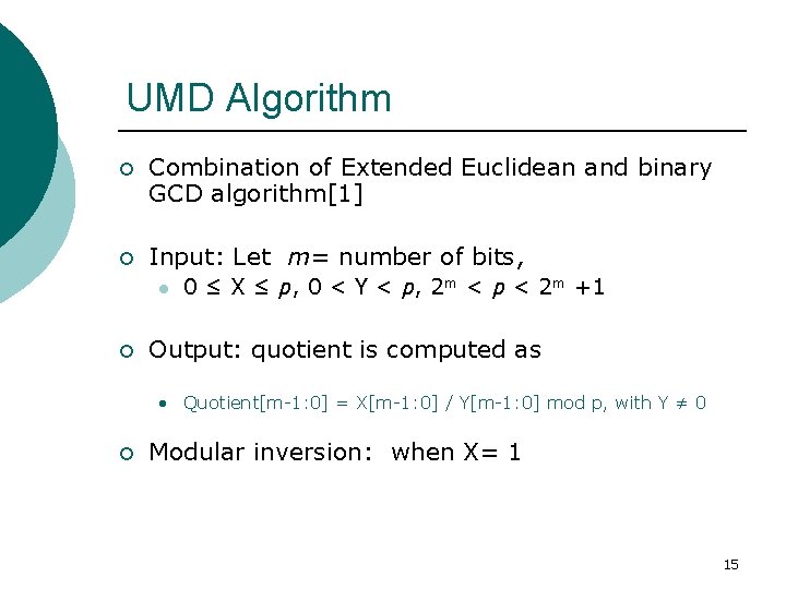
UMD Algorithm ¡ Combination of Extended Euclidean and binary GCD algorithm[1] ¡ Input: Let m= number of bits, l ¡ 0 ≤ X ≤ p, 0 < Y < p, 2 m < p < 2 m +1 Output: quotient is computed as • Quotient[m-1: 0] = X[m-1: 0] / Y[m-1: 0] mod p, with Y ≠ 0 ¡ Modular inversion: when X= 1 15

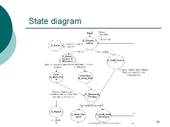
Pseudocode Inputs: X, Y, p c = Y, u = X, d = p, w = 0, g = 0 WHILE c != 0 IF co = 0 THEN /* co: Least significant bit of c */ c : = c/2 g : = g-1 ELSE IF g < 0 THEN SWAP(c, d), SWAP(u, w), g : = -g ENDIF; k = 1 IF ((c+d) mod 4 ≠ 0) THEN k = -1 ELSE g: = g -1 ENDIF; c : = (c + k*d)/2, u = (u+ k*w) ENDIF u : = (u + uo* p)/2 /* uo: Least significant bit of u */ END WHILE IF d = 1 THEN Quotient : = w ELSE Quotient : = p - w ENDIF 16
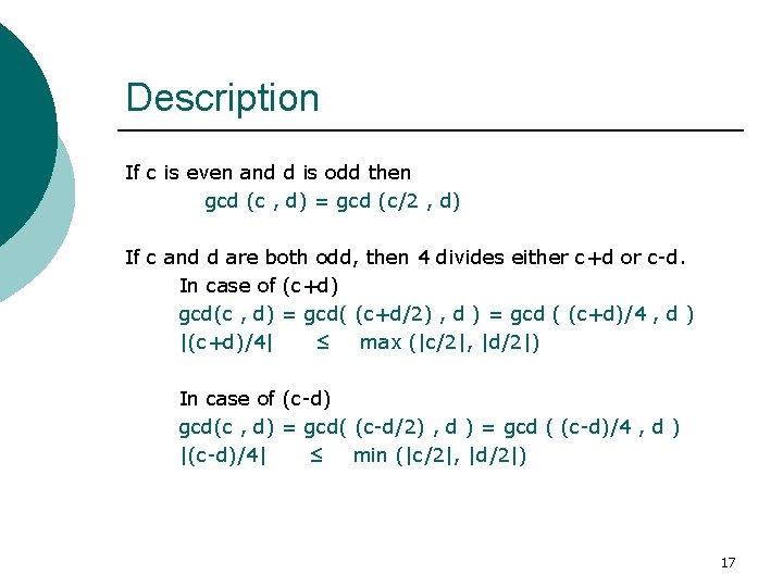
Description If c is even and d is odd then gcd (c , d) = gcd (c/2 , d) If c and d are both odd, then 4 divides either c+d or c-d. In case of (c+d) gcd(c , d) = gcd( (c+d/2) , d ) = gcd ( (c+d)/4 , d ) |(c+d)/4| ≤ max (|c/2|, |d/2|) In case of (c-d) gcd(c , d) = gcd( (c-d/2) , d ) = gcd ( (c-d)/4 , d ) |(c-d)/4| ≤ min (|c/2|, |d/2|) 17
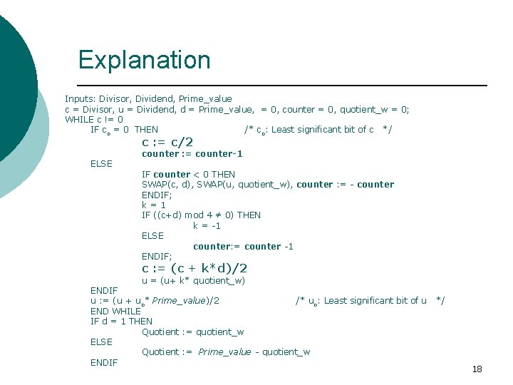
Explanation Inputs: Divisor, Dividend, Prime_value c = Divisor, u = Dividend, d = Prime_value, = 0, counter = 0, quotient_w = 0; WHILE c != 0 IF co = 0 THEN /* co: Least significant bit of c */ c : = c/2 ELSE counter : = counter-1 IF counter < 0 THEN SWAP(c, d), SWAP(u, quotient_w), counter : = - counter ENDIF; k = 1 IF ((c+d) mod 4 ≠ 0) THEN k = -1 ELSE counter: = counter -1 ENDIF; c : = (c + k*d)/2 u = (u+ k* quotient_w) ENDIF u : = (u + uo* Prime_value)/2 /* uo: Least significant bit of u */ END WHILE IF d = 1 THEN Quotient : = quotient_w ELSE Quotient : = Prime_value - quotient_w ENDIF 18
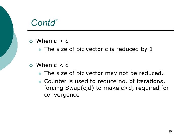
Contd’ ¡ When c > d l The size of bit vector c is reduced by 1 ¡ When c < d l The size of bit vector may not be reduced. l Counter is used to reduce no. of iterations, forcing Swap(c, d) to make c>d, required for convergence 19

Contd’ ¡ ¡ ¡ At any point l w*Y = d*X (modp) l u*Y = c*X (modp) always hold Start of Iterations l w=0, d=p; 0*Y = X*p mod(p)=0 End of Iterations l c=0, d=± 1, w=Z , gcd(Y, p) =1 l Z*Y = X mod(p) l => Z=X/Y mod(p) 20
State diagram 21
Design Flow l. Define requirements: specify functionality of device. E. g: I/O and performance requirements l. C coding: Source code of a program that implements a Finite field divider. l. Verilog coding entry: functional description of architectures. Include combinational logic design and RTL (Register Transfer Level) coding. l. Synthesis: generates a netlist from Define Requirements C coding Verify Logic Verilog Coding Verify Logic Synthesis the Verilog code. Netlist is a low level abstraction of the code. l. Place and Route: determines the Verify Logic Place & Route placement of each cell and connections between cells in the chip. l. Configuration: a process in which the circuit design (bitstream file) is downloaded into the FPGA. Verify Logic Configuration FPGA Chip 22
C Code Implementation ¡ Source code of a program that implements the divider using UMD algorithm ¡ Verification purposes 23

Consultation Session Example: X=98; Y=11; P=103 Quotient =37 98/11 mod(103)=37 98= (37*11) mod (103) = 98 Outputs of C Code 24
Design Flow l. Define requirements: specify functionality of device. E. g: I/O and performance requirements l. C coding: Source code of a program that implements a Finite field divider. l. Verilog coding entry: functional description of architectures. Include combinational logic design and RTL (Register Transfer Level) coding. l. Synthesis: generates a netlist from Define Requirements C coding Verify Logic Verilog Coding Verify Logic Synthesis the Verilog code. Netlist is a low level abstraction of the code. l. Place and Route: determines the Verify Logic Place & Route placement of each cell and connections between cells in the chip. l. Configuration: a process in which the circuit design (bitstream file) is downloaded into the FPGA. Verify Logic Configuration FPGA Chip 25
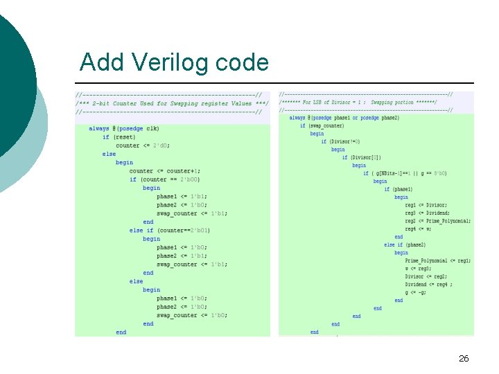
Add Verilog code 26
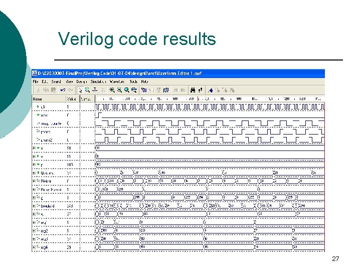
Verilog code results . 27
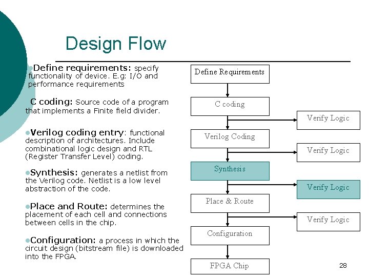
Design Flow l. Define requirements: specify functionality of device. E. g: I/O and performance requirements l. C coding: Source code of a program that implements a Finite field divider. l. Verilog coding entry: functional description of architectures. Include combinational logic design and RTL (Register Transfer Level) coding. l. Synthesis: generates a netlist from Define Requirements C coding Verify Logic Verilog Coding Verify Logic Synthesis the Verilog code. Netlist is a low level abstraction of the code. l. Place and Route: determines the Verify Logic Place & Route placement of each cell and connections between cells in the chip. l. Configuration: a process in which the circuit design (bitstream file) is downloaded into the FPGA. Verify Logic Configuration FPGA Chip 28
Implementation ¡ FPGA design for primary divider 29
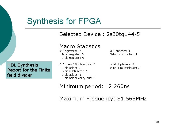
Synthesis for FPGA Selected Device : 2 s 30 tq 144 -5 Macro Statistics HDL Synthesis Report for the Finite field divider # Registers: 14 1 -bit register: 5 8 -bit register: 9 # Counters: 1 3 -bit up counter: 1 # Adders/ Subtractors: 6 8 -bit adder: 3 8 -bit subtractor: 1 9 -bit adder carry out: 1 # Multiplexers: 3 2 -to-1 multiplexer: 3 Minimum period: 12. 260 ns Maximum Frequency: 81. 566 MHz 30
Overview ¡ Problem description l l l ¡ ¡ Related work My contribution l l l ¡ ¡ ¡ Finite field Representing Alpha values Finite/Galois field algebra Division algorithms Efficient hardware requirements Project phases Design flow UMD Algorithm, pseudocode, description, state diagram C code implementation Verilog code results & timing diagram Implementation, synthesis for a FPGA (Field Programmable Gate Array) Conclusion Future work References 31
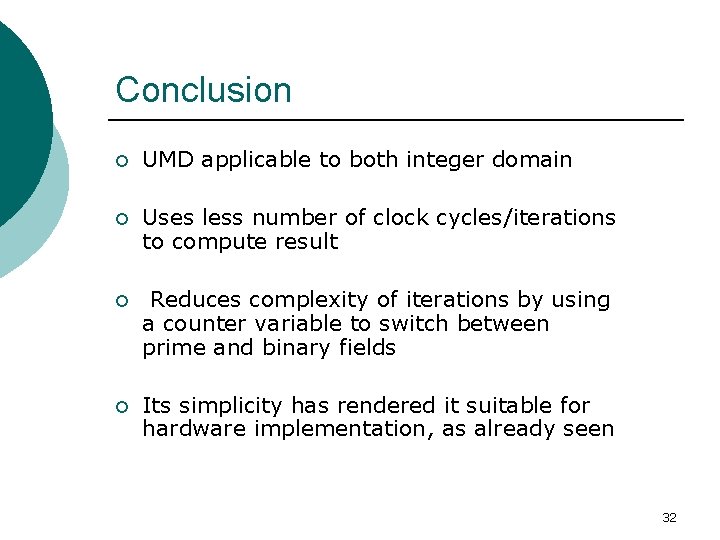
Conclusion ¡ UMD applicable to both integer domain ¡ Uses less number of clock cycles/iterations to compute result ¡ Reduces complexity of iterations by using a counter variable to switch between prime and binary fields ¡ Its simplicity has rendered it suitable for hardware implementation, as already seen 32
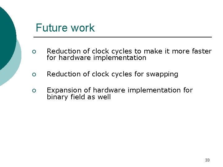
Future work ¡ Reduction of clock cycles to make it more faster for hardware implementation ¡ Reduction of clock cycles for swapping ¡ Expansion of hardware implementation for binary field as well 33
References ¡ J. Guajardo and C. Paar, “Itoh-Tsuji Inversion in Standard Basis and Its Applications in Cryptography and Codes, ” and Christof Paar, “Inversion in Finite Fields and Rings” , Designs, Codes and Cryptography, 25, app. 207 -216, 2002. ¡ A. F. Tenca, L. A. Tawalbeh (School of Electrical Engineering and Computer Sciences, Oregon State University, USA), “Algorithm for unified modular division in GF(p) and GF(2 n) suitable for cryptographic hardware”, Electronics Letters, March 2004, Vol. 40 No. 5 ¡ IEEE P 1363 / D 13, Standard Specifications for Public Key Cryptography, copyright © 1999 by the Institute of Electrical and Electronics Engineers, Inc. 345 East 47 th Street, New York, NY 10017, USA ¡ http: //www. math. sc. edu/~sumner/numbertheory/euclidean. html ¡ Shu Lin/ Daniel J. Costello, Jr. , Error Control Coding: Fundamentals and Applications, Prentice Hall Series in Computer Applications in Electrical Engineering, Franklin F. Kuo Editor ¡ Chin-Liang Wang and Jung-Lung Lin, “A Systolic Architecture for Computing Inverses and Divisions in Finite Fields GF(2 m)”, IEEE Log Number 9207282, Dec. 19, 1990; revised July 1, 1992, Department of Electrical Engineering, National Tsing Hua University, Hsinchu, Taiwan, Republic of China. 34
¡ ¡ Chien-Hsing Wu, Chien-Ming Wu, Ming-Der Shieh, and Yin-Tsung Hwang, “High. Speed, Low-Complexity Systolic Designs of Novel Iterative Division Algorithms in GF(2 m)”, IEEE transactions on Computers, Vol. 53, No. 3, March 2004. S. C. Shantz. “From Euclid's GCD to Montgomery Multiplication to the Great Divide". Technical Report TR-2001 -95, Sun Microsystems Laboratories, 2001. 4, 7 Savas, E. , and Koc, C. K. “Architectures for unified field inversion with applications in elliptic curve cryptography” 9 th IEEE Intl. Conf. on Electronics, Circuits and System – ICECS’ 2002, Dubrovnik, Croatia, September 2002 Clifford E. Cummings, “Non Blocking Assignments in Verilog Synthesis, Coding Styles That Kill”, Sunburst Design, Inc. cliffc@sunburst-design. com : web site: www. sunburst-design. com/papers VHDL & RTL Books ¡ Lionel Bening and Harry Foster, Principles of Verifiable RTL Design, A Functional Coding Style Supporting Verification Processes in Verilog, Kluwer Academic Publishers ¡ J. Bhasker, Verilog VHDL Synthesis, A Practical Primer, Star Galaxy Publishing, Lucent Technologies 1998 35

Thankyou Questions ? ?
- Slides: 36