Fourier Ptychographic Microscopy at Telecommunication Wavelength Using a

- Slides: 1

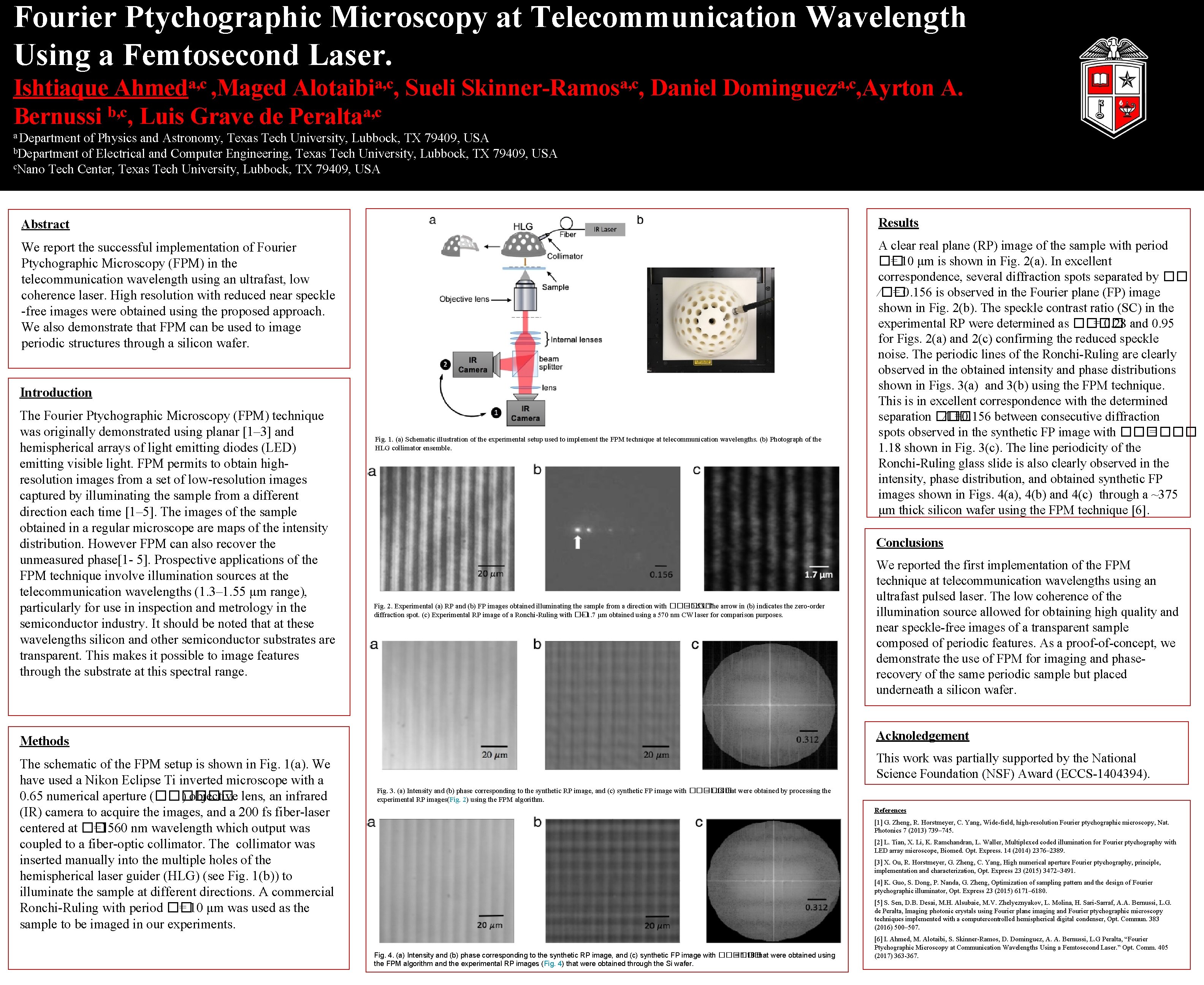
Fourier Ptychographic Microscopy at Telecommunication Wavelength Using a Femtosecond Laser. a, c Ahmed , Maged a, c Alotaibi , Ishtiaque Sueli b, c a, c Bernussi , Luis Grave de Peralta a, c Skinner-Ramos , Daniel a, c Dominguez , Ayrton A. a Department of Physics and Astronomy, Texas Tech University, Lubbock, TX 79409, USA b. Department of Electrical and Computer Engineering, Texas Tech University, Lubbock, TX 79409, USA c. Nano Tech Center, Texas Tech University, Lubbock, TX 79409, USA Abstract Results We report the successful implementation of Fourier Ptychographic Microscopy (FPM) in the telecommunication wavelength using an ultrafast, low coherence laser. High resolution with reduced near speckle -free images were obtained using the proposed approach. We also demonstrate that FPM can be used to image periodic structures through a silicon wafer. A clear real plane (RP) image of the sample with period �� = 10 μm is shown in Fig. 2(a). In excellent correspondence, several diffraction spots separated by �� ∕�� = 0. 156 is observed in the Fourier plane (FP) image shown in Fig. 2(b). The speckle contrast ratio (SC) in the experimental RP were determined as ���� = 0. 28 and 0. 95 for Figs. 2(a) and 2(c) confirming the reduced speckle noise. The periodic lines of the Ronchi-Ruling are clearly observed in the obtained intensity and phase distributions shown in Figs. 3(a) and 3(b) using the FPM technique. This is in excellent correspondence with the determined separation �� ∕�� =0. 156 between consecutive diffraction spots observed in the synthetic FP image with ������ = 1. 18 shown in Fig. 3(c). The line periodicity of the Ronchi-Ruling glass slide is also clearly observed in the intensity, phase distribution, and obtained synthetic FP images shown in Figs. 4(a), 4(b) and 4(c) through a ~375 μm thick silicon wafer using the FPM technique [6]. Introduction The Fourier Ptychographic Microscopy (FPM) technique was originally demonstrated using planar [1– 3] and hemispherical arrays of light emitting diodes (LED) emitting visible light. FPM permits to obtain highresolution images from a set of low-resolution images captured by illuminating the sample from a different direction each time [1– 5]. The images of the sample obtained in a regular microscope are maps of the intensity distribution. However FPM can also recover the unmeasured phase[1 - 5]. Prospective applications of the FPM technique involve illumination sources at the telecommunication wavelengths (1. 3– 1. 55 μm range), particularly for use in inspection and metrology in the semiconductor industry. It should be noted that at these wavelengths silicon and other semiconductor substrates are transparent. This makes it possible to image features through the substrate at this spectral range. Fig. 1. (a) Schematic illustration of the experimental setup used to implement the FPM technique at telecommunication wavelengths. (b) Photograph of the HLG collimator ensemble. Conclusions Fig. 2. Experimental (a) RP and (b) FP images obtained illuminating the sample from a direction with ������ = 0. 53. The arrow in (b) indicates the zero-order diffraction spot. (c) Experimental RP image of a Ronchi-Ruling with �� = 1. 7 μm obtained using a 570 nm CW laser for comparison purposes. We reported the first implementation of the FPM technique at telecommunication wavelengths using an ultrafast pulsed laser. The low coherence of the illumination source allowed for obtaining high quality and near speckle-free images of a transparent sample composed of periodic features. As a proof-of-concept, we demonstrate the use of FPM for imaging and phaserecovery of the same periodic sample but placed underneath a silicon wafer. Methods Acknoledgement The schematic of the FPM setup is shown in Fig. 1(a). We have used a Nikon Eclipse Ti inverted microscope with a 0. 65 numerical aperture (������ ) objective lens, an infrared (IR) camera to acquire the images, and a 200 fs fiber-laser centered at �� =1560 nm wavelength which output was coupled to a fiber-optic collimator. The collimator was inserted manually into the multiple holes of the hemispherical laser guider (HLG) (see Fig. 1(b)) to illuminate the sample at different directions. A commercial Ronchi-Ruling with period �� = 10 μm was used as the sample to be imaged in our experiments. This work was partially supported by the National Science Foundation (NSF) Award (ECCS-1404394). Fig. 3. (a) Intensity and (b) phase corresponding to the synthetic RP image, and (c) synthetic FP image with ������ = 1. 18 that were obtained by processing the experimental RP images(Fig. 2) using the FPM algorithm. References [1] G. Zheng, R. Horstmeyer, C. Yang, Wide-field, high-resolution Fourier ptychographic microscopy, Nat. Photonics 7 (2013) 739– 745. [2] L. Tian, X. Li, K. Ramchandran, L. Waller, Multiplexed coded illumination for Fourier ptychography with LED array microscope, Biomed. Opt. Express. 14 (2014) 2376– 2389. [3] X. Ou, R. Horstmeyer, G. Zheng, C. Yang, High numerical aperture Fourier ptychography, principle, implementation and characterization, Opt. Express 23 (2015) 3472– 3491. [4] K. Guo, S. Dong, P. Nanda, G. Zheng, Optimization of sampling pattern and the design of Fourier ptychographic illuminator, Opt. Express 23 (2015) 6171– 6180. [5] S. Sen, D. B. Desai, M. H. Alsubaie, M. V. Zhelyeznyakov, L. Molina, H. Sari-Sarraf, A. A. Bernussi, L. G. de Peralta, Imaging photonic crystals using Fourier plane imaging and Fourier ptychographic microscopy techniques implemented with a computercontrolled hemispherical digital condenser, Opt. Commun. 383 (2016) 500– 507. Fig. 4. (a) Intensity and (b) phase corresponding to the synthetic RP image, and (c) synthetic FP image with ������ = 1. 18 that were obtained using the FPM algorithm and the experimental RP images (Fig. 4) that were obtained through the Si wafer. [6] I. Ahmed, M. Alotaibi, S. Skinner-Ramos, D. Dominguez, A. A. Bernussi, L. G Peralta, “Fourier Ptychographic Microscopy at Communication Wavelengths Using a Femtosecond Laser. ” Opt. Comm. 405 (2017) 363 -367.