Formal Design and Verification of an Asynchronous SRAM

![Summary ■ An alternative to [Baz et al. ] design of an asynchronous SRAM Summary ■ An alternative to [Baz et al. ] design of an asynchronous SRAM](https://slidetodoc.com/presentation_image_h/f776110e560271506b32bbfd64a25f4e/image-15.jpg)

- Slides: 17

Formal Design and Verification of an Asynchronous SRAM Controller Victor Khomenko, Andrey Mokhov, Danil Sokolov, Alex Yakovlev

Motivation ■ SRAM is a ubiquitous component – so must be robust and efficient ■ Advantages of asynchronous SRAM: – reliable operation under a wide range of supply voltages – can trade off energy for performance (essential for lowpower devices, e. g. powered by energy harvesters) ■ Fascinating challenge for the application of formal models of concurrency! 2

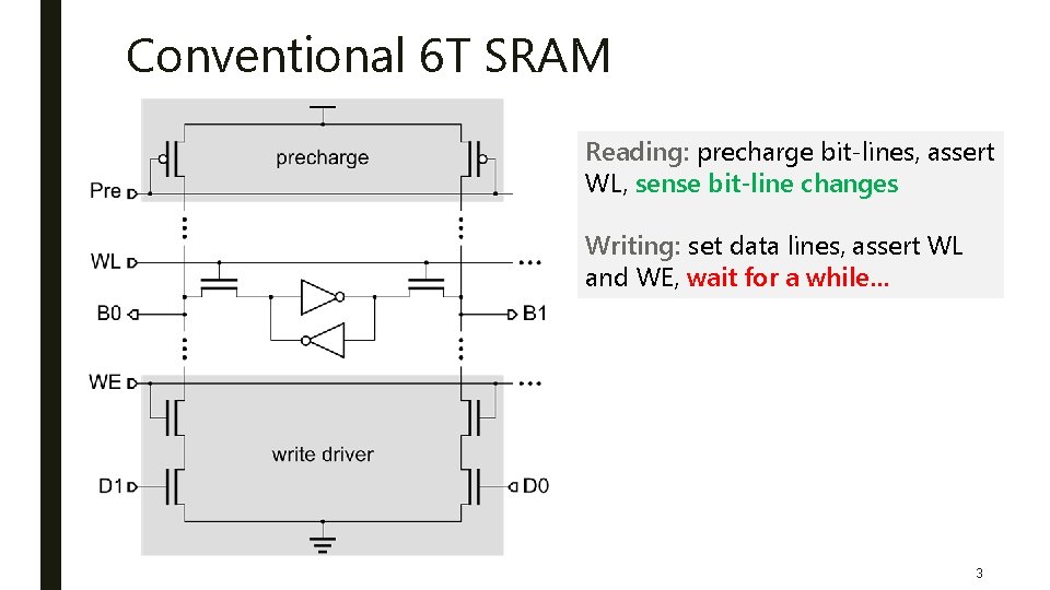
Conventional 6 T SRAM Reading: precharge bit-lines, assert WL, sense bit-line changes Writing: set data lines, assert WL and WE, wait for a while… 3

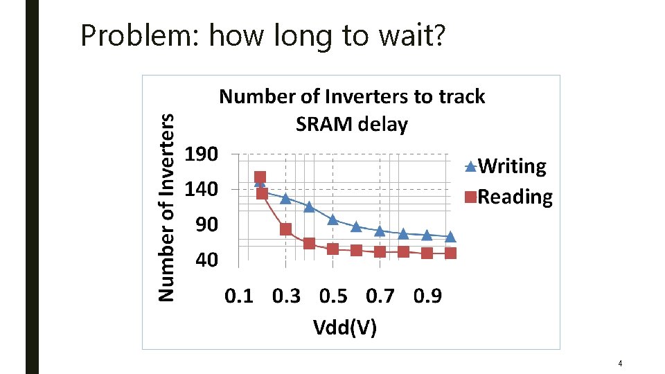
Problem: how long to wait? 4

Previous work ■ Using non-standard memory cells – Extra transistors, and – Extra bit-lines or acknowledgement lines ■ Different delay lines for different voltages – Voltage references ■ Duplicating an SRAM line to act as a reference delay line 5

Previous work (cont’d) ■ Async solution with completion detection – developed by A. Baz et al. (PATMOS 2010, JOLPE 2011) based on the original idea of V. Varshavsky (USSR Patent, 1988) – no voltage references – speed-independent, but – interface to bit-lines is not delay-insensitive ■ less robust in the low-power mode, especially if bit-lines are buffered or augmented with a sense amplifier ■ Completion detection in write mode idea: – easy when the bit is flipped – read before writing to check if the bit needs flipping 6

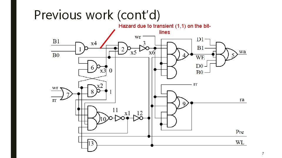
Previous work (cont’d) Hazard due to transient (1, 1) on the bitlines 7

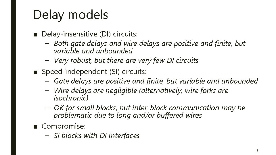
Delay models ■ Delay-insensitive (DI) circuits: – Both gate delays and wire delays are positive and finite, but variable and unbounded – Very robust, but there are very few DI circuits ■ Speed-independent (SI) circuits: – Gate delays are positive and finite, but variable and unbounded – Wire delays are negligible (alternatively, wire forks are isochronic) – OK for small blocks, but inter-block communication may be problematic due to long and/or buffered wires ■ Compromise: – SI blocks with DI interfaces 8

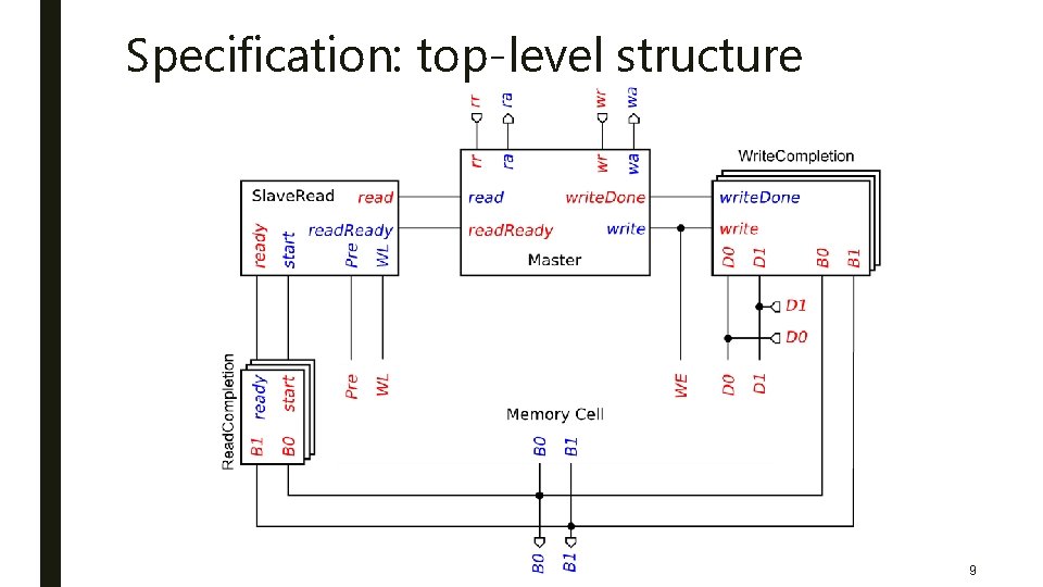
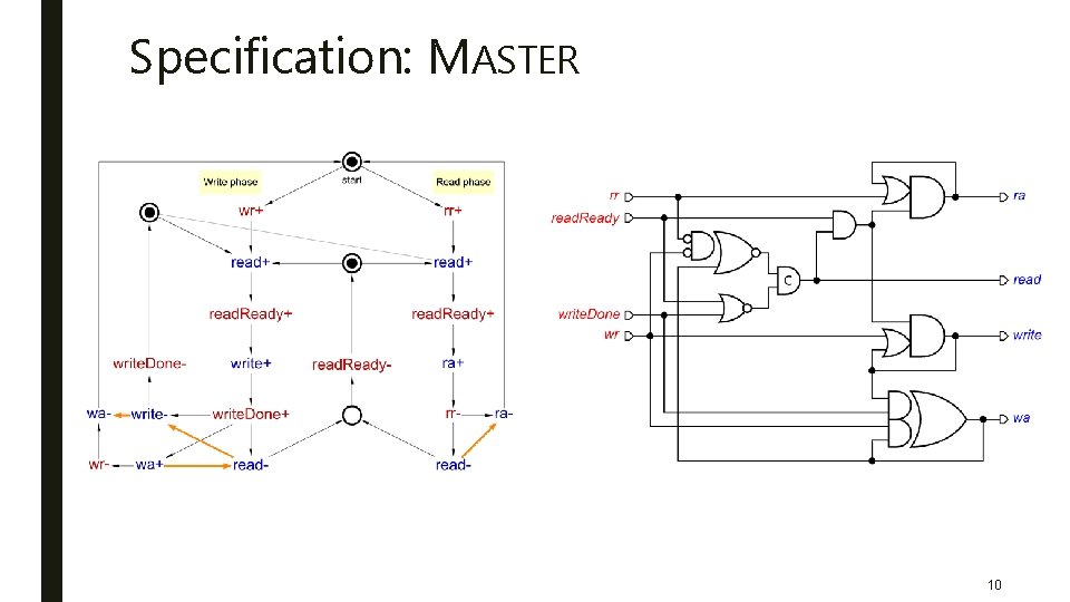
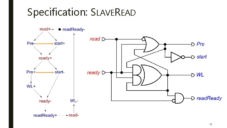
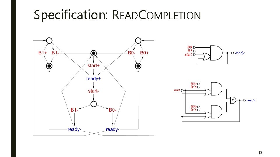
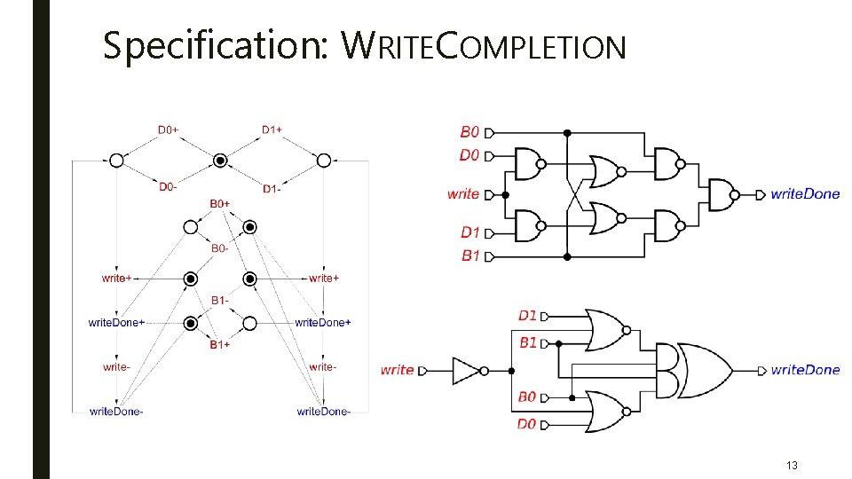
Specification: top-level structure 9

Specification: MASTER 10

Specification: SLAVEREAD 11

Specification: READCOMPLETION 12

Specification: WRITECOMPLETION 13

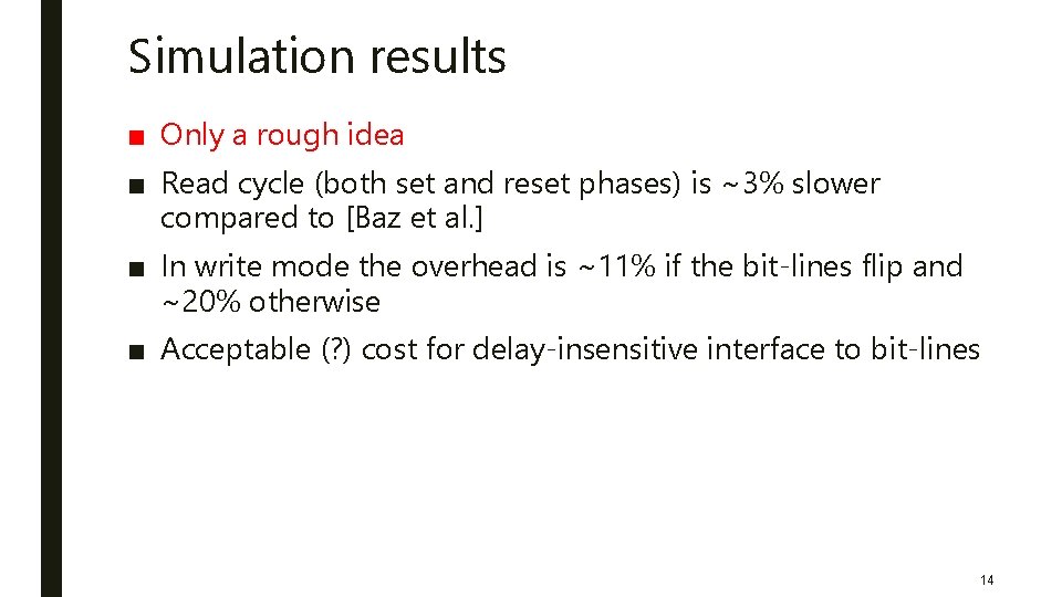
Simulation results ■ Only a rough idea ■ Read cycle (both set and reset phases) is ~3% slower compared to [Baz et al. ] ■ In write mode the overhead is ~11% if the bit-lines flip and ~20% otherwise ■ Acceptable (? ) cost for delay-insensitive interface to bit-lines 14
![Summary An alternative to Baz et al design of an asynchronous SRAM Summary ■ An alternative to [Baz et al. ] design of an asynchronous SRAM](https://slidetodoc.com/presentation_image_h/f776110e560271506b32bbfd64a25f4e/image-15.jpg)
Summary ■ An alternative to [Baz et al. ] design of an asynchronous SRAM controller – delay-insensitive interface to bit-lines – performance overhead is small ■ Systematically designed ■ Formally verified ■ The design flow is supported by: workcraft. org 15

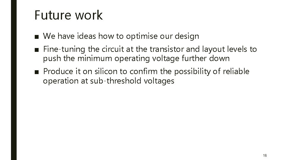
Future work ■ We have ideas how to optimise our design ■ Fine-tuning the circuit at the transistor and layout levels to push the minimum operating voltage further down ■ Produce it on silicon to confirm the possibility of reliable operation at sub-threshold voltages 16

Thank you! Any questions? 17