FMC adapter status Luis Miguel Jara Casas 5092017


 is included in the SCC")

")
 uses RJ")


- Slides: 21
FMC adapter status Luis Miguel Jara Casas 5/09/2017
FMC adapter: Connection with PCIe in XPress. K 7 board, from FPGA(no room for cables) ~7 mm ~18 mm JTAG ~ 20 mm ~ 17 mm DP 2 FMC connector DP 1 RJ 45 ~ 20 mm LEMO § § § § AC coupling Signal multiplexing Level converters Regulators Clock generation ADC EEPROM … LEMO ~7 mm 2
Status: DP 1 DP 2 LEMO RJ 45 JTAG FMC connector Interface Display. Ports-FMC connector: • Ongoing • Some doubts about multiplexing of signals, AC coupling and signal integrity depending on final SCC pinout. Lemo connectors interface with FMC connector: DONE RJ 45 interface with FMC connector: DONE JTAG interface with FMC: to be decided which JTAG connector to use. Ongoing, pending to close depending on the decisions for Display. Ports. Clock generation in FMC Two clocks added (GTXs reference and one for the general fabric), I 2 C programmable, more clocks can be added under request. EEPROM included for compliance with other boards. 3
Display. Ports Interface Display. Ports with FMC adapter: • Taking as a reference the DRAFT schematics of SCC (below): some data lanes are also used for external clocks (serializer and CMD clock). • Study of the proposal of being able to use the same Display. Port connector on the DAQ side for both CMD+DATA as well as CLK+HIT_OR from firmware. In order to multiplex this signals in the FMC board via firmware, high speed bidirectional analog switches are needed: • Data are CML while external clocks are LVDS. • Data and clocks have different directions. Display. Port pinout in SCC draft version 4
Display. Ports Interface Display. Ports with FMC adapter: • Taking as a reference the DRAFT schematics of SCC (below): some data lanes are also used for external clocks (serializer and CMD clock). • Study of the proposal of being able to use the same Display. Port connector on the DAQ side for both CMD+DATA as well as CLK+HIT_OR from firmware. FMC adapter card SCC LEMO JTAG DP 2 FMC connector DP 1 RJ 45 LEMO 5
Display. Ports One level of switches in two data pairs: • First one in order to provide flexibility from firmware point of view, being able to use both Display. Ports in the FMC adapter for CMD+DATA or CLK+HIT_OR • Second in order to be able to provide external serializer and command clock in some of the data lanes (in two of the high speed differential pairs). SCC FPGA FMC adapter card DP 1 TX DATA or HIT_OR High speed analog switch AC coupling CML buffer CML DATA GTX LVDS Sel 2 LVDS Buffer In order to provide flexibility and choose from firmware which DP connector goes to which SCC DP connector HIT_OR RX 6
Display. Ports Two levels of switches in two data pairs: • First one in order to provide flexibility from firmware point of view, being able to use both Display. Ports in the FMC adapter for CMD+DATA or CLK+HIT_OR • Second in order to be able to provide external serializer and command clock in some of the data lanes (in two of the high speed differential pairs). SCC FPGA FMC adapter card High speed bidirectional analog switch Clock Buffer LVDS DP 1 TX Sel 1 DATA or HIT_OR EXT_CLK (SER, CMD) High speed analog switch AC coupling CML buffer CML DATA LVDS Sel 2 Buffer In order to provide flexibility and choose from firmware which DP connector goes to which SCC DP connector GTX HIT_OR RX 7
Display. Ports Display. Port pinout in SCC draft version Problems and questions of this configuration: • AC coupling after the analog switches (operating range of analog switches can be exceeded if used in SP chains). • Signal integrity of the data lanes: § Ron of high speed bidirectional switches around 8Ω. § Possible parasitic C and L in this switches. § Layout: routing more complex. § Recommendations from signal integrity experts at CERN: data lanes the most straight forward connected to multi-gigabit transceivers. If signal integrity is a real problem, possible solutions: • Giving up to the flexibility of being able to choose which Display. Port in the FMC adapter goes with which one in the SCC would provide two data lanes without any analog switch interface. The multiplexing could be implemented with jumpers if needed. • Give up with that flexibility just for one of the HIT_OR pairs, HITOR 3, so GTX 0 doesn’t go through any analog switch. 8
Display. Port: NTC • Negative Temperature Coefficient thermistor (NTC) is included in the SCC card and connected to pins 13 and 14 of DP 1 in SCC card. • In the FMC adapter card, the voltage drop in this resistor is amplified and the output is ADC converted. • Converter is controlled via I 2 C. NTC pins (coming from Display. Port) Resistor network and amplifier of voltage drop 4 channel 12 bit ADC control and readout via I 2 C FMC connector 9
Clock generation in FMC adapter • Clock resources in XPress. K 7 are not enough. • Also a clock reference is needed for GTXs PLLs. • A clock multiplier is included in the FMC adapter, with two clock outputs available: § One connected to GTX clock reference pin. § The second connected to MRCC driver in FPGA for general purpose. • The output frequency can be programmed via I 2 C • Clocks can be synchronized with an external signal if needed. Sync clock Crystal oscillator x 2 Clock multiplier CLK_GEN_PURPOSE FMC connector CLK_GTX_REF Frequency programming for each output channel via I 2 C • Clock output can be programmed from 0. 001 to 1028 MHz • It fulfils the clock requirements needed for clock reference signals on GTXs (see back-up slides) 10
Trigger IO 4 x LEMO: • 4 Lemo connectors (2 RX and 2 TX) connected to a transceiver with configurable voltage translation. • MMC 3 taken as a reference FMC connector LEMO 4 -Bit Dual. Supply Bus Transceiver With Configurable Voltage Translation LEMO TX TX RX RX Voltage selection with jumpers 11
Trigger IO FMC connector RJ 45: • EUDET Telescope family (test-beam infrastructure) uses RJ 45 connectors for trigger and handshake communication with the telescope/trigger devices. • MMC 3 taken as a reference Drivers and receivers RJ 45 12
EEPROM FMC connector • Included just in case the adapter is used with a Xilinx evaluation board for FMC Standard compliance (VITA 57. 1). • For these boards, the EEPROM is queried at power on. Problems detecting the presence of an FMC mezzanine in case not mounted. • Not need to be mounted for other boards. ADC control and readout via I 2 C EEPROM memory Write protection via jumpers 13
JTAG • From RD 53 A, all JTAG pads are pulled-up or down ON-CHIP according to the standard, except the test reset pad TRST_B. • Pending to decide which JTAG connector type. FMC connector • Pinout of the FMC connector takes into account the resources of the Xpress. K 7 (allocation of different drivers, power sources, clock capable pins…) • Some pins in Column J are avoided as they are non-FMC compliant signals in the XPress. K 7. • Pinout changes depending on topics discussed previously. Layout • Layout will be done by CERN PCB workshop and reviewed by ourselves once a stable version of the schematics is finished. 14
Thank you! 15
Backup slides 16
Clock reference for MGTs: • MGTs in XPress. K 7 board are already connected to oscillators, needed as a reference, but in the case of the MGTs connected to the FMC, no oscillator is mounted. Oscillator used as a clock reference for MGTs connected to PCIe The oscillator connected to the quad MGT bank that is wired to the FMC connector is not mounted (but clock of the previous MGT bank can be used, 100 MHz, external clock can source up to 3 GTX quads)
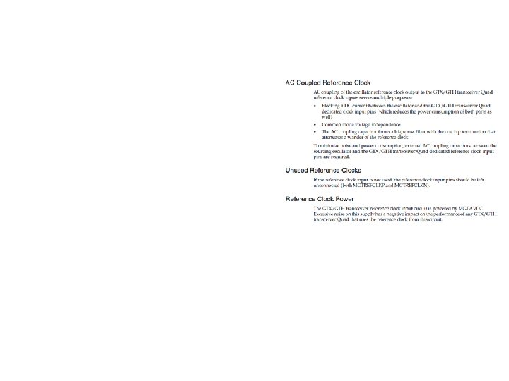
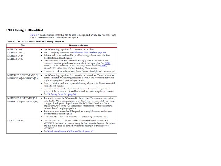
• Jitter on the reference clock has a disastrous effect on the channel’s quality, can be far worse than poor a poor PCB layout. • QPLL and CPLL locks in the reference clock, so jitter on the reference clock results in jitter in the serial data clock. • The prevailing effect is in the transmitter, which relies on this serial data clock. • The receiver is mainly based on the clock it recovers from the incoming data stream, so it is less sensitive to jitter. • Transceiver reference clock checklist from Xilinx 7 series FPGAs GTX/GTH Transceivers User Guide (UG 476)
• VOLTAGE SWING of the reference clock: -0. 5 V min, 1. 32 V max • REFERENCE CLOCK characteristics: OURS is -2 (DS 182 Xilinx data sheet)