Floating point processor for Programmable calculator Vikas Kumar
Floating point processor for Programmable calculator Vikas Kumar Sharma Saurabh Gupta Mentors: Veeramani V. , Abhinav Agarwal June 14, 2006 EE Summer Camp 2006 1
Outline n n IEEE 754 standard Floating Point Arithmetic q q q n Processor Design q q n n Addition & Subtraction Multiplication & Division Exceptions Instruction Set Architecture (ISA) Processor units FPGA implementation Conclusion Future work References June 14, 2006 EE Summer Camp 2006 2
Introduction n n Floating point Calculator design Standard used: IEEE 754 Operations implemented: - Addition, Subtraction, Multiplication, Division User programs in hex using simple assembly instructions June 14, 2006 EE Summer Camp 2006 3
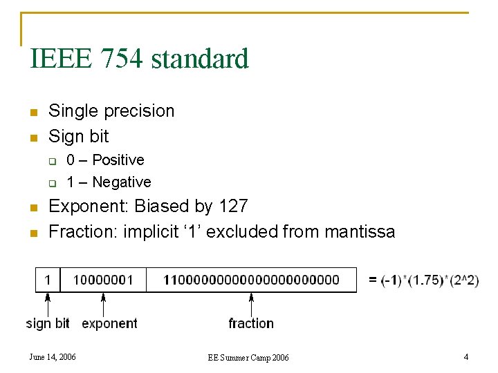
IEEE 754 standard n n Single precision Sign bit q q n n 0 – Positive 1 – Negative Exponent: Biased by 127 Fraction: implicit ‘ 1’ excluded from mantissa June 14, 2006 EE Summer Camp 2006 4
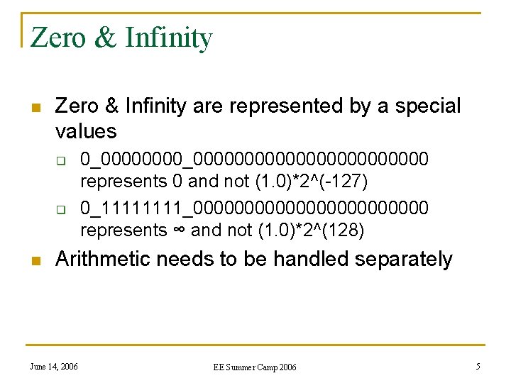
Zero & Infinity n Zero & Infinity are represented by a special values q q n 0_000000000000000 represents 0 and not (1. 0)*2^(-127) 0_1111_000000000000 represents ∞ and not (1. 0)*2^(128) Arithmetic needs to be handled separately June 14, 2006 EE Summer Camp 2006 5
Arithmetic Algorithms n n Addition Subtraction Multiplication Division June 14, 2006 EE Summer Camp 2006 6
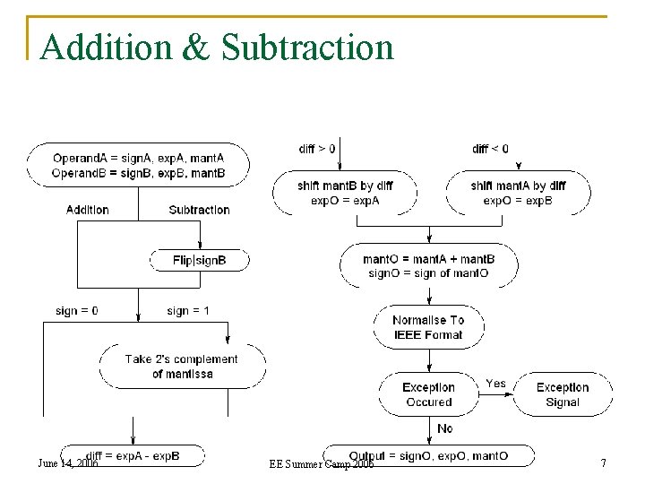
Addition & Subtraction June 14, 2006 EE Summer Camp 2006 7
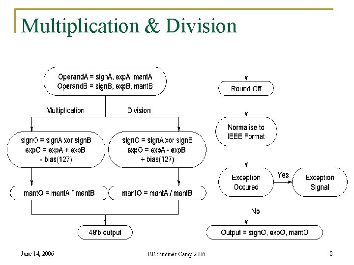
Multiplication & Division June 14, 2006 EE Summer Camp 2006 8
Normalization to IEEE 754 n n 0. 0000101000000… * 2^(128) Normalized as 1. 010000… * 2^(123) q n How? q q n We need implicit ‘ 1’ in the IEEE 754 format Leading Zero Counter Barrel Shifter Both these modules are combinatorial June 14, 2006 EE Summer Camp 2006 9
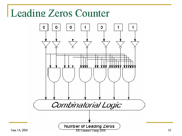
Leading Zeros Counter June 14, 2006 EE Summer Camp 2006 10
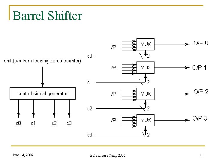
Barrel Shifter June 14, 2006 EE Summer Camp 2006 11
Exceptions Behavior n Exceptions Implemented q q n Out of Bound Invalid operation Operation suspended & FPGA LED blink June 14, 2006 EE Summer Camp 2006 12
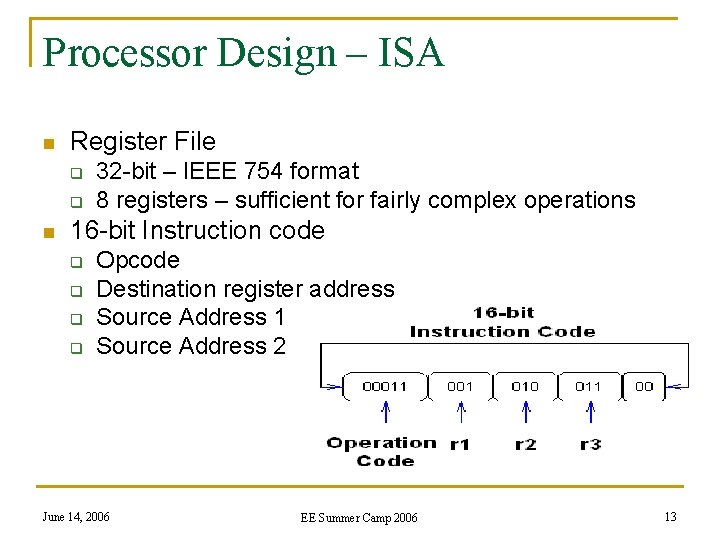
Processor Design – ISA n Register File q q n 32 -bit – IEEE 754 format 8 registers – sufficient for fairly complex operations 16 -bit Instruction code q q Opcode Destination register address Source Address 1 Source Address 2 June 14, 2006 EE Summer Camp 2006 13
Instructions n Arithmetic operations – 16 bit, 3 register addresses q q n n Add Subtract Multiply Divide Move – 48 bit, 1 register address Termination instruction – 16 bit, all zeros June 14, 2006 EE Summer Camp 2006 14
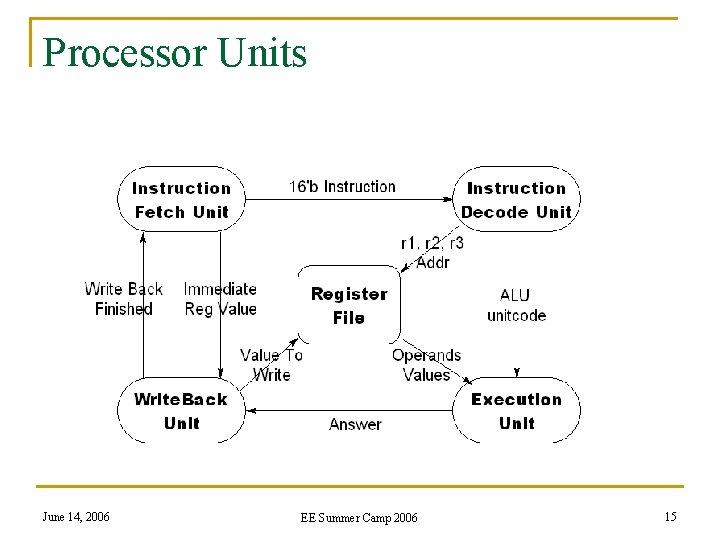
Processor Units June 14, 2006 EE Summer Camp 2006 15
Processor Units… n Instruction Fetch Unit (IF) q q n Starts on reset with counter value zero Fetches instruction to decoder or register file depending on the instruction type Instruction Decode Unit (ID) q q Starts at the finish of IF Passes proper ALU unit code to execution module and register addresses to register file June 14, 2006 EE Summer Camp 2006 16
Processor Units… n Execution Unit (EX) q q q n Starts at the data read signal from register file Operands passed to FPU with a activation signal to the required arithmetic unit Gives the result to Write Back Unit in IEEE 754 format Write Back Unit (WB) q q Starts at the finished execution signal from EX Selects between the result and the input data depending upon the instruction code June 14, 2006 EE Summer Camp 2006 17
Simulation of FPU n n Appropriate test benches were used for simulation and design was verified Exception behavior was checked June 14, 2006 EE Summer Camp 2006 18
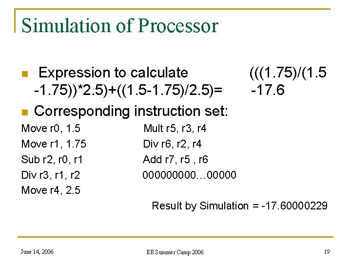
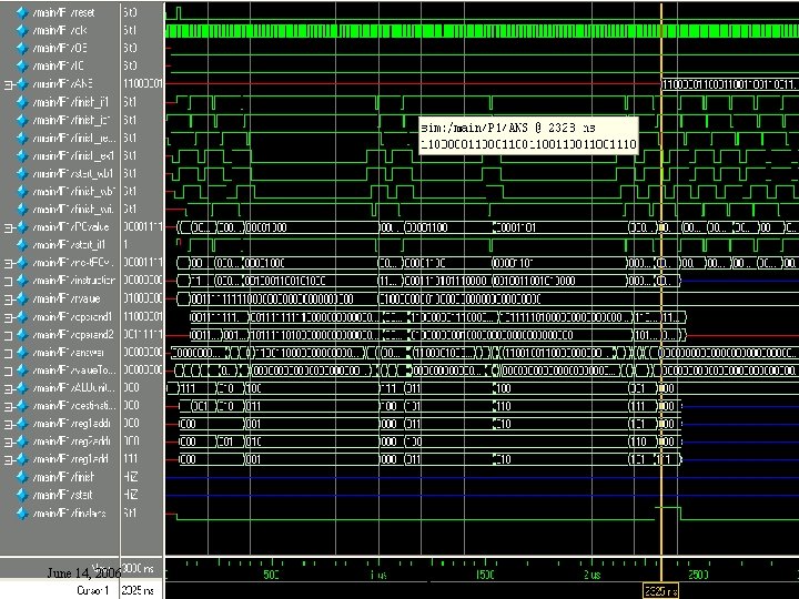
Simulation of Processor n n Expression to calculate -1. 75))*2. 5)+((1. 5 -1. 75)/2. 5)= Corresponding instruction set: Move r 0, 1. 5 Move r 1, 1. 75 Sub r 2, r 0, r 1 Div r 3, r 1, r 2 Move r 4, 2. 5 (((1. 75)/(1. 5 -17. 6 Mult r 5, r 3, r 4 Div r 6, r 2, r 4 Add r 7, r 5 , r 6 00000… 00000 Result by Simulation = -17. 60000229 June 14, 2006 EE Summer Camp 2006 19
June 14, 2006 EE Summer Camp 2006 20
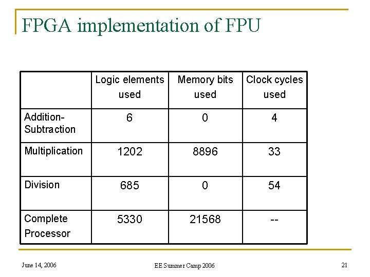
FPGA implementation of FPU Addition. Subtraction Multiplication Division Complete Processor June 14, 2006 Logic elements used Memory bits used Clock cycles used 6 0 4 1202 8896 33 685 0 54 5330 21568 -- EE Summer Camp 2006 21
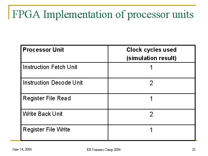
FPGA Implementation of processor units Processor Unit Clock cycles used (simulation result) Instruction Fetch Unit 1 Instruction Decode Unit 2 Register File Read 1 Write Back Unit 2 Register File Write 1 June 14, 2006 EE Summer Camp 2006 22
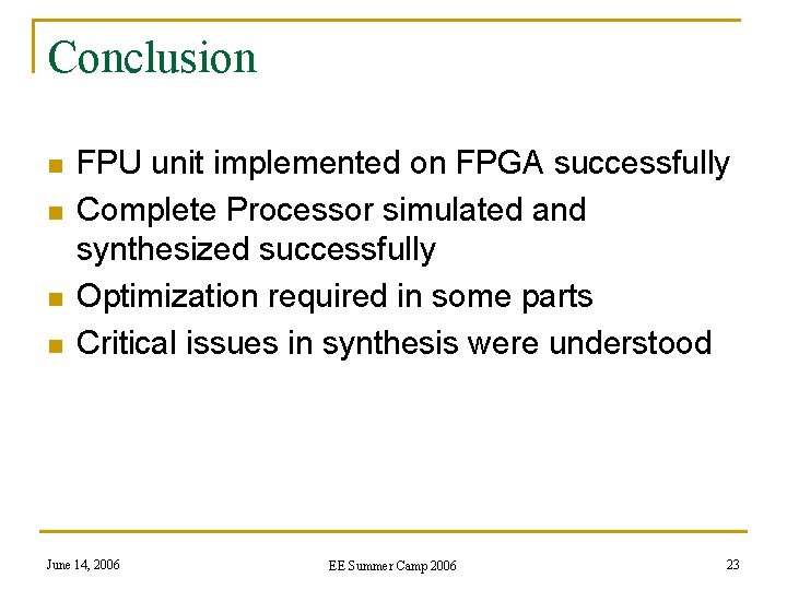
Conclusion n n FPU unit implemented on FPGA successfully Complete Processor simulated and synthesized successfully Optimization required in some parts Critical issues in synthesis were understood June 14, 2006 EE Summer Camp 2006 23
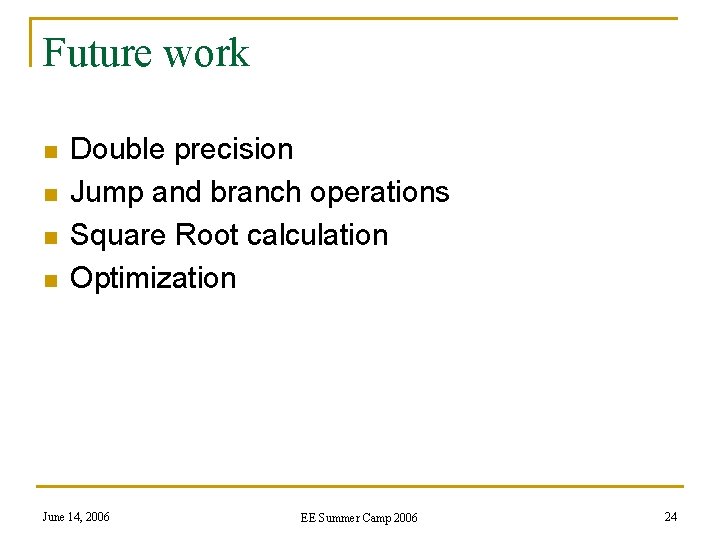
Future work n n Double precision Jump and branch operations Square Root calculation Optimization June 14, 2006 EE Summer Camp 2006 24
References 1. 2. 3. 4. Institute of Electrical and Electronics Engineers, ”IEEE Standard for Binary Floating-Point Arithmetic”, ANSI/IEEE Standard 754 -1985, August 1985 http: //docs. sun. com/source/806 -3568/ncg goldberg. html http: //en. wikipedia. org/wiki/Booth’s multiplication algorithm http: //www. cs. wisc. edu/ smoler/x 86 text/lect. notes/arith. flpt. html June 14, 2006 EE Summer Camp 2006 25
Thank you June 14, 2006 EE Summer Camp 2006 26
- Slides: 26