FlipFlops Reference Chapter 5 Sequential Circuits Moris Mano







- Slides: 46

Flip-Flops Reference: Chapter 5 Sequential Circuits Moris Mano 4 th Ediditon

Revision

Types of Logic Circuits 1. Combinational Logic Circuits 2. Sequential Circuits

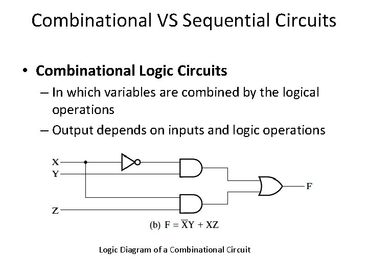
Combinational VS Sequential Circuits • Combinational Logic Circuits – In which variables are combined by the logical operations – Output depends on inputs and logic operations Logic Diagram of a Combinational Circuit

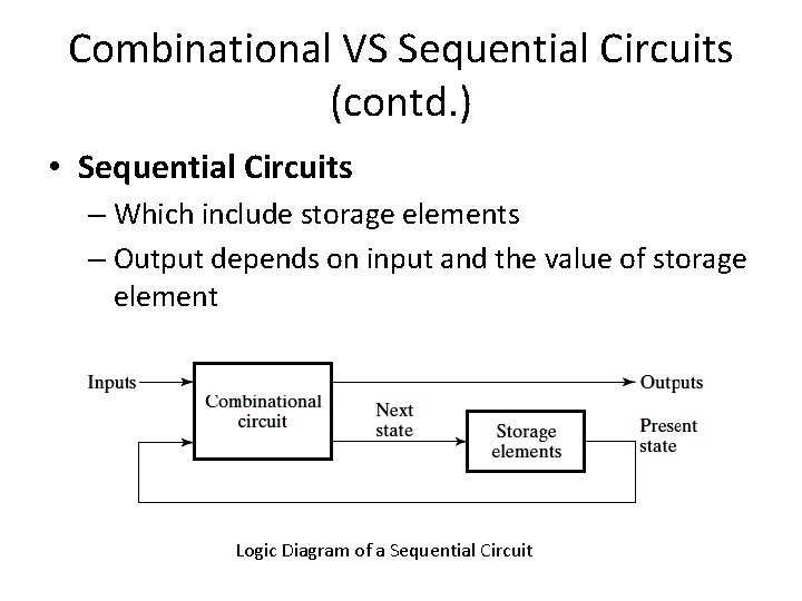
Combinational VS Sequential Circuits (contd. ) • Sequential Circuits – Which include storage elements – Output depends on input and the value of storage element Logic Diagram of a Sequential Circuit

Storage Element • Storage elements are circuits • that store binary information for indefinite time • Can change their state(value stored) on the basis of input signal

Latches

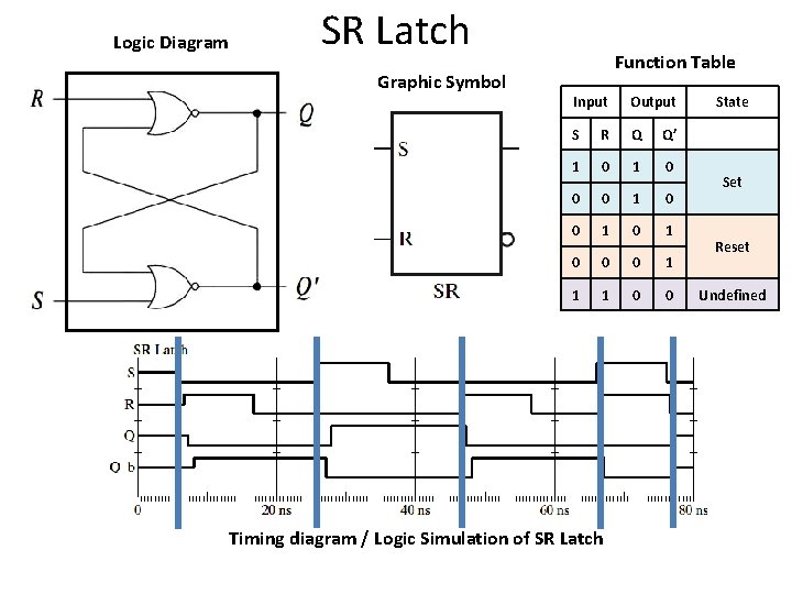
Logic Diagram SR Latch Graphic Symbol Function Table Input Output S R Q Q’ 1 0 0 0 1 0 1 0 0 0 1 1 1 0 0 Timing diagram / Logic Simulation of SR Latch State Set Reset Undefined

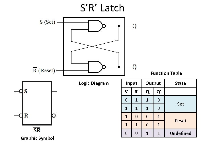
S’R’ Latch Function Table Logic Diagram Graphic Symbol Input Output S’ R’ Q Q’ 0 1 1 1 0 1 0 0 1 1 State Set Reset Undefined

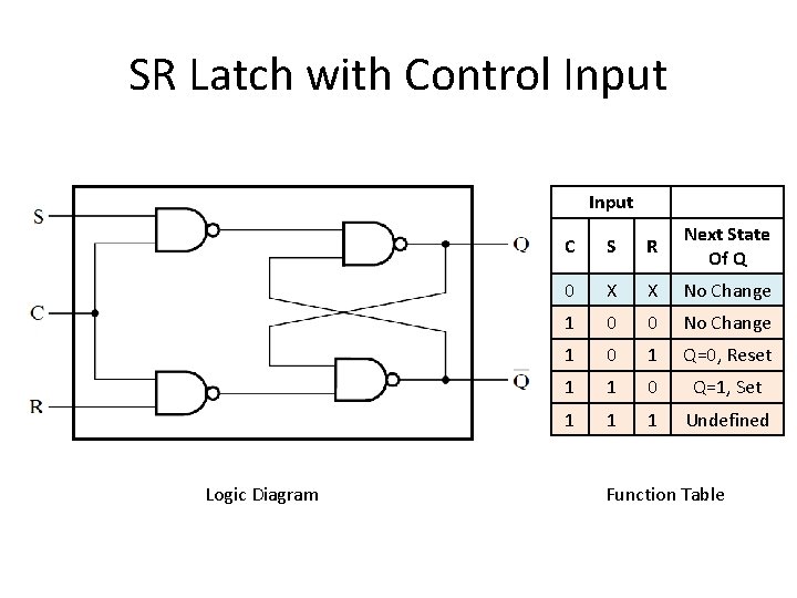
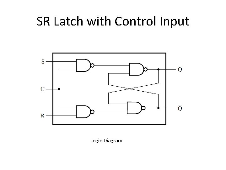
SR Latch with Control Input Logic Diagram C S R Next State Of Q 0 X X No Change 1 0 0 No Change 1 0 1 Q=0, Reset 1 1 0 Q=1, Set 1 1 1 Undefined Function Table

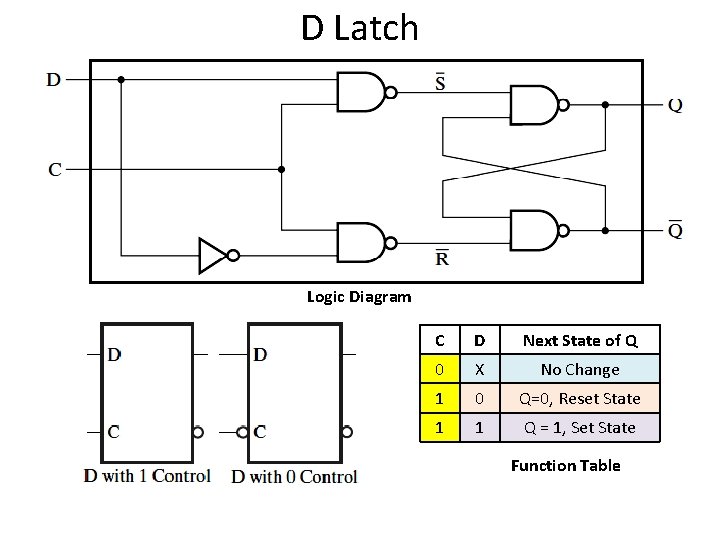
D Latch Logic Diagram C D Next State of Q 0 X No Change 1 0 Q=0, Reset State 1 1 Q = 1, Set State Function Table

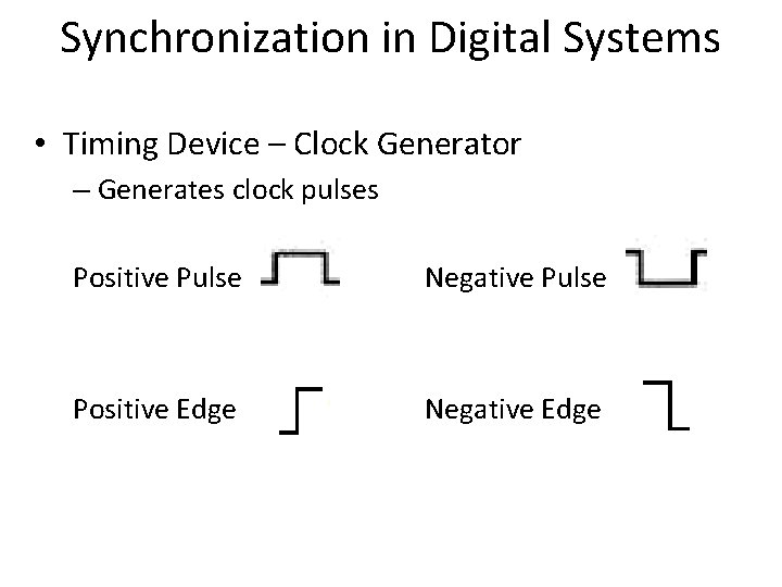
Synchronization in Digital Systems • Timing Device – Clock Generator – Generates clock pulses Positive Pulse Negative Pulse Positive Edge Negative Edge

Synchronization in Digital Systems • Clock as control input of Latches • Problem with Latches – Transparency • Solution Flip-Flops

Flip-Flop

Types of Flip-Flops 1. Pulse-Triggered Flip-Flops 2. Edge-Triggered Flip-Flops

Pulse-Triggered Flip-Flop

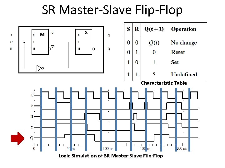
SR Master-Slave Flip-Flop M S Characteristic Table Logic Simulation of SR Master-Slave Flip-Flop

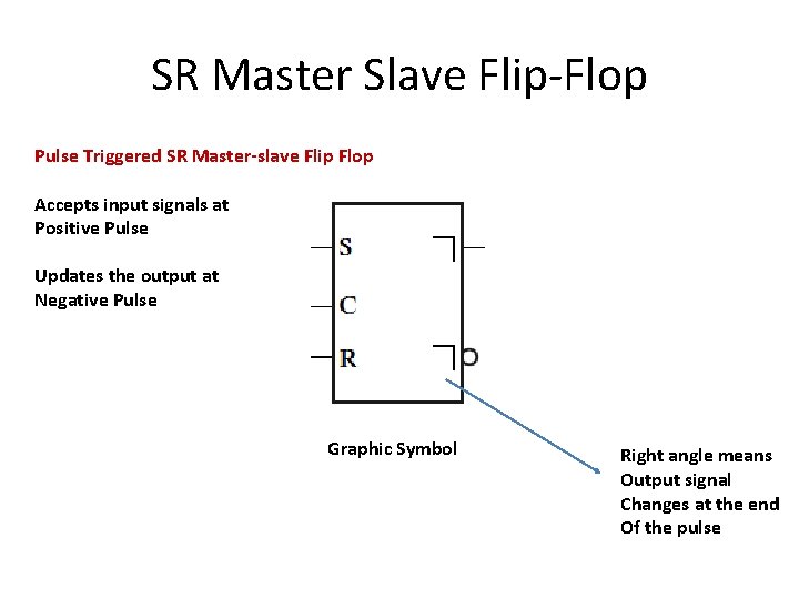
SR Master Slave Flip-Flop Pulse Triggered SR Master-slave Flip Flop Accepts input signals at Positive Pulse Updates the output at Negative Pulse Graphic Symbol Right angle means Output signal Changes at the end Of the pulse

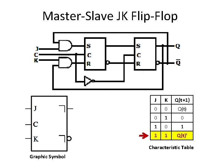
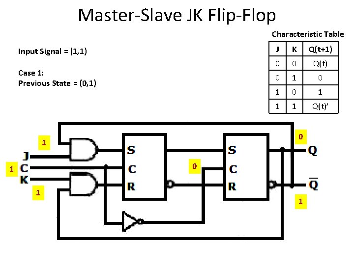
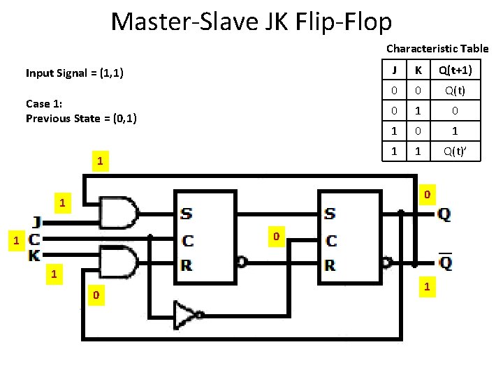
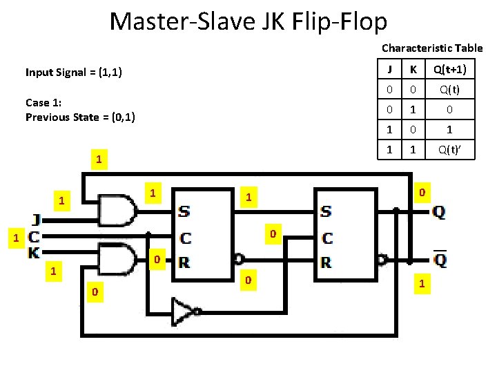
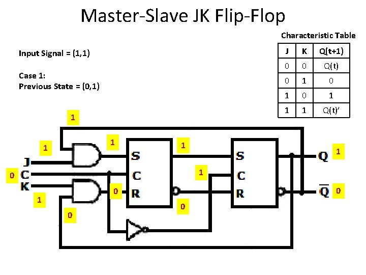
Master-Slave JK Flip-Flop J K Q(t+1) 0 0 Q(t) 0 1 0 1 1 1 Q(t)’ Characteristic Table Graphic Symbol

Master-Slave JK Flip-Flop Characteristic Table Input Signal = (1, 1) Case 1: Previous State = (0, 1) 1 J K Q(t+1) 0 0 Q(t) 0 1 0 1 1 1 Q(t)’ 0 1 1 1

Master-Slave JK Flip-Flop Characteristic Table Input Signal = (1, 1) Case 1: Previous State = (0, 1) J K Q(t+1) 0 0 Q(t) 0 1 0 1 1 1 Q(t)’ 0 1 1 1

Master-Slave JK Flip-Flop Characteristic Table Input Signal = (1, 1) Case 1: Previous State = (0, 1) 1 J K Q(t+1) 0 0 Q(t) 0 1 0 1 1 1 Q(t)’ 0 1 1 0 1

Master-Slave JK Flip-Flop Characteristic Table Input Signal = (1, 1) Case 1: Previous State = (0, 1) Which means save 1 1 K Q(t+1) 0 0 Q(t) 0 1 0 1 1 1 Q(t)’ 0 1 1 J 0 1 0 1

Master-Slave JK Flip-Flop Characteristic Table Input Signal = (1, 1) Case 1: Previous State = (0, 1) 1 1 1 J K Q(t+1) 0 0 Q(t) 0 1 0 1 1 1 Q(t)’ 0 1 0 1 0 0 1

Master-Slave JK Flip-Flop Characteristic Table Input Signal = (1, 1) Case 1: Previous State = (0, 1) 1 1 J K Q(t+1) 0 0 Q(t) 0 1 0 1 1 1 Q(t)’ 1 1 0 0 0 1 0 0

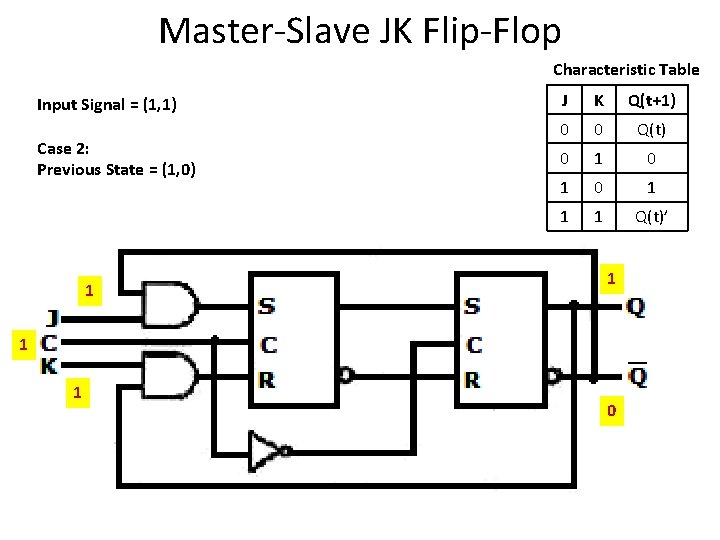
Master-Slave JK Flip-Flop Characteristic Table Input Signal = (1, 1) Case 2: Previous State = (1, 0) 1 J K Q(t+1) 0 0 Q(t) 0 1 0 1 1 1 Q(t)’ 1 1 1 0

Master-Slave JK Flip-Flop Characteristic Table Input Signal = (1, 1) Case 2: Previous State = (1, 0) J K Q(t+1) 0 0 Q(t) 0 1 0 1 1 1 Q(t)’ 1 1 0

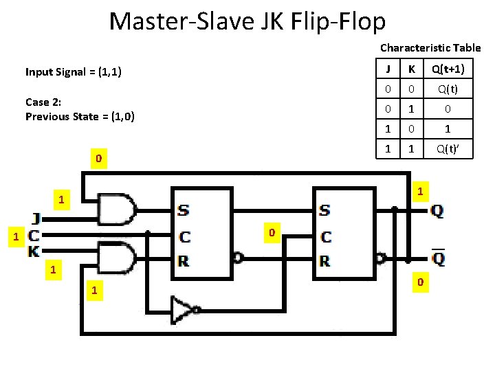
Master-Slave JK Flip-Flop Characteristic Table Input Signal = (1, 1) Case 2: Previous State = (1, 0) 0 J K Q(t+1) 0 0 Q(t) 0 1 0 1 1 1 Q(t)’ 1 1 0 1 1 1 0

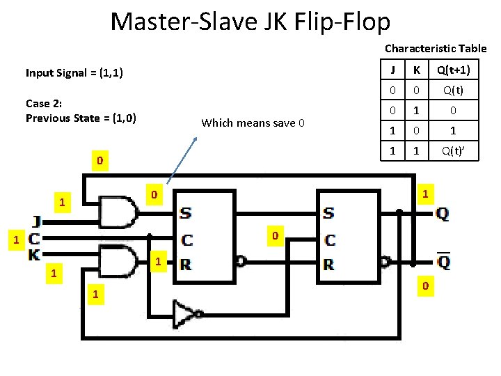
Master-Slave JK Flip-Flop Characteristic Table Input Signal = (1, 1) Case 2: Previous State = (1, 0) Which means save 0 0 K Q(t+1) 0 0 Q(t) 0 1 0 1 1 1 Q(t)’ 1 0 1 J 0 1 1 0

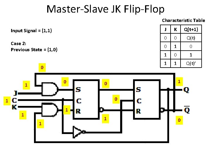
Master-Slave JK Flip-Flop Characteristic Table Input Signal = (1, 1) Case 2: Previous State = (1, 0) 0 0 1 J K Q(t+1) 0 0 Q(t) 0 1 0 1 1 1 Q(t)’ 1 0 0 1 1 1 0

Master-Slave JK Flip-Flop Characteristic Table Input Signal = (1, 1) Case 2: Previous State = (1, 0) 0 0 1 0 J K Q(t+1) 0 0 Q(t) 0 1 0 1 1 1 Q(t)’ 0 1 1 1

Test Your Concepts • Can you fix the undefined state problem in SR and S’R’ latches?

Pulse-Triggered Flip-Flop vs Edge-Triggered Flip-Flop

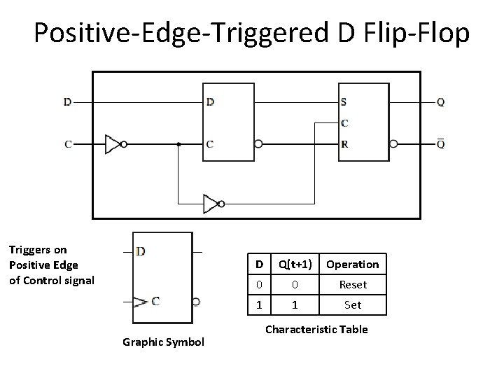
Positive-Edge-Triggered D Flip-Flop Triggers on Positive Edge of Control signal Graphic Symbol D Q(t+1) Operation 0 0 Reset 1 1 Set Characteristic Table

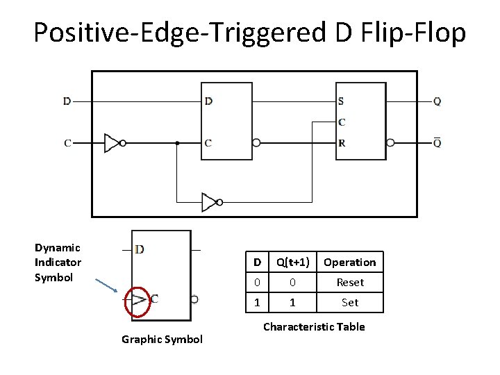
Positive-Edge-Triggered D Flip-Flop Dynamic Indicator Symbol Graphic Symbol D Q(t+1) Operation 0 0 Reset 1 1 Set Characteristic Table

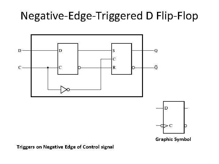
Negative-Edge-Triggered D Flip-Flop Graphic Symbol Triggers on Negative Edge of Control signal

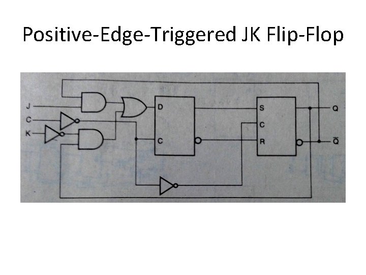
Positive-Edge-Triggered JK Flip-Flop

Equations of Flip-Flops

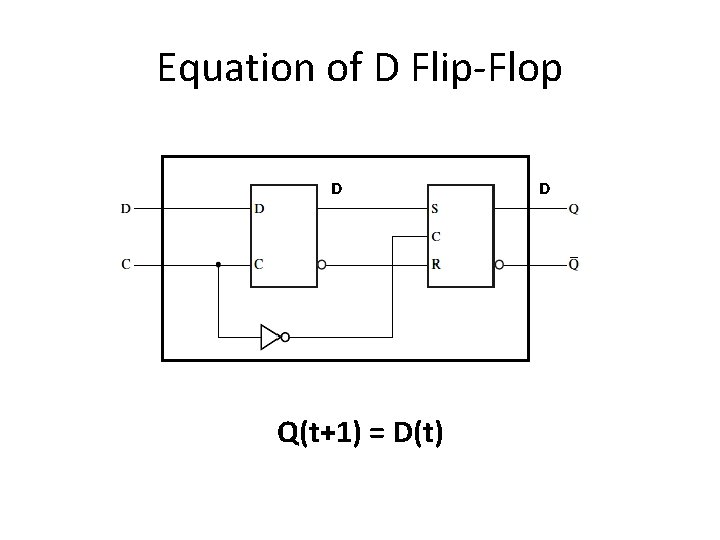
Equation of D Flip-Flop D Q(t+1) = D(t) D

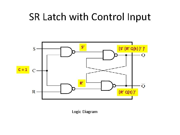
SR Latch with Control Input Logic Diagram

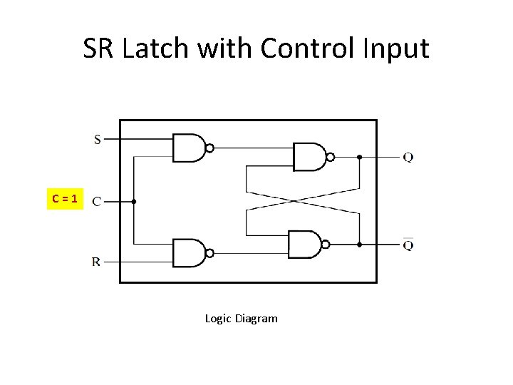
SR Latch with Control Input C=1 Logic Diagram

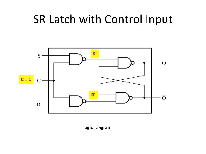
SR Latch with Control Input S’ C=1 R’ Logic Diagram

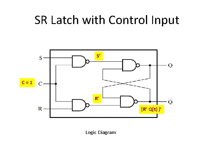
SR Latch with Control Input S’ C=1 R’ (R’ Q(t) )’ Logic Diagram

SR Latch with Control Input S’ (R’ Q(t) )’ )’ C=1 R’ (R’ Q(t) )’ Logic Diagram

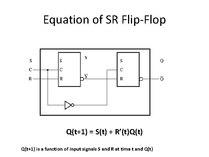
Equation of SR Flip-Flop Q(t+1) = S(t) + R’(t)Q(t) Q(t+1) is a function of input signals S and R at time t and Q(t)

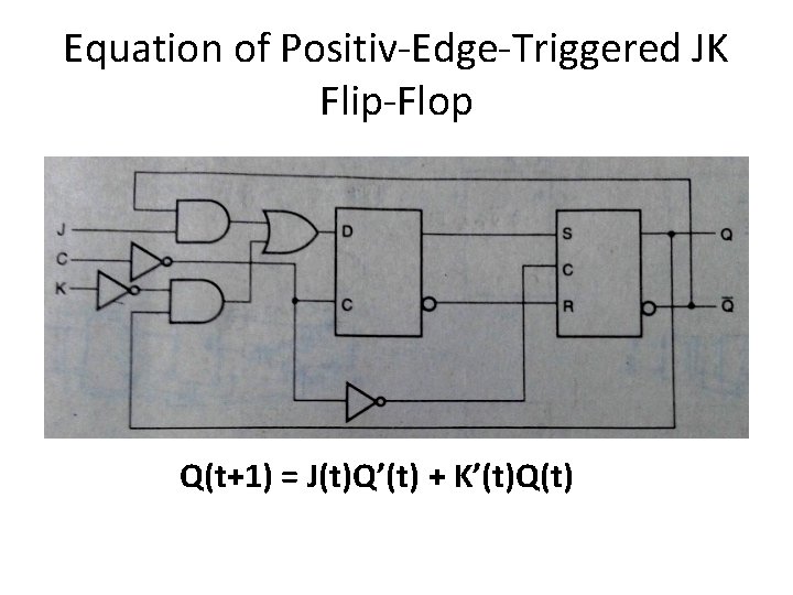
Equation of Positiv-Edge-Triggered JK Flip-Flop Q(t+1) = J(t)Q’(t) + K’(t)Q(t)