FlipFlops and Related Devices WenHung Liao Ph D
- Slides: 39

Flip-Flops and Related Devices Wen-Hung Liao, Ph. D.

Objectives l l l l l Recognize the various IEEE/ANSI flip-flop symbols. Use state transition diagrams to describe counter operation. Use flip-flops in synchronization circuits. Connect shift registers as data transfer circuits. Employ flip-flops as frequency-division and counting circuits. Understand the typical characteristics of Schmitt triggers. Apply two different types of one-shots in circuit design. Design a free-running oscillator using a 555 timer. Recognize and predict the effects of clock skew on synchronous circuits.

Clocked Flip-Flops l l l Controlled inputs + CLK Setup and Hold times Clocked S-C Flip-Flop Clocked J-K Flip-Flop Clocked D Flip-Flop

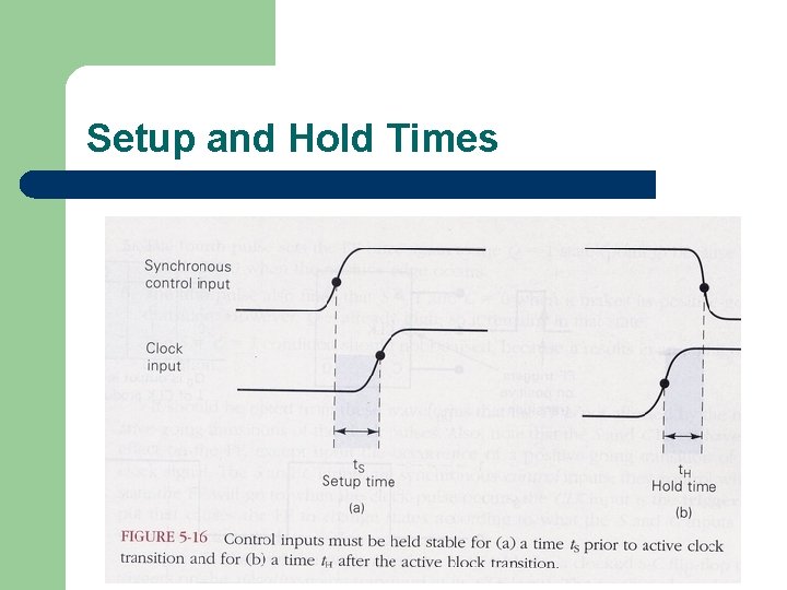
Setup and Hold Times

Setup and Hold Times (cont’d) l l The setup time ts is the time interval immediately proceeding the active transition of the CLK signal during which the control input signal must be maintained at the proper level. The hold time t. H, is the time interval immediately following the active transition of the CLK signal during which the control input signal must be maintained at the proper level.

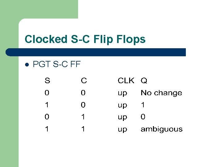
Clocked S-C Flip Flops l PGT S-C FF

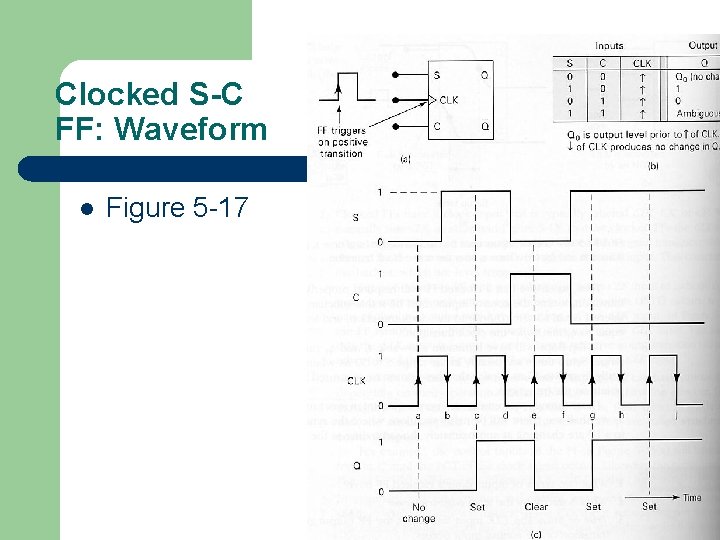
Clocked S-C FF: Waveform l Figure 5 -17

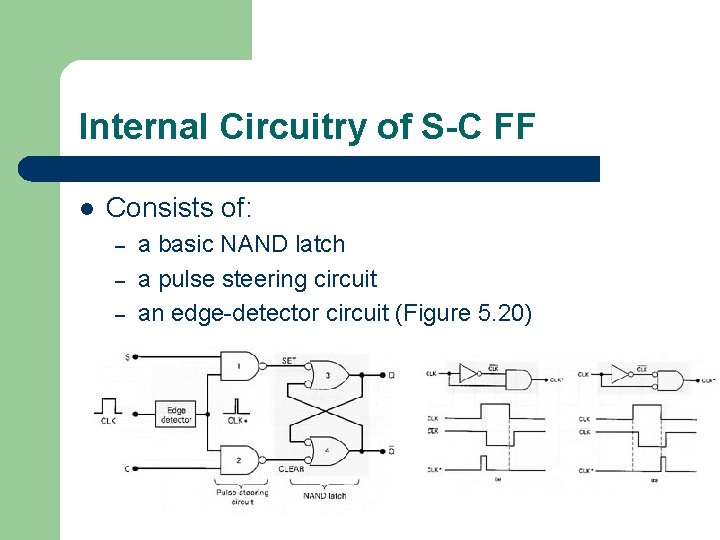
Internal Circuitry of S-C FF l Consists of: – – – a basic NAND latch a pulse steering circuit an edge-detector circuit (Figure 5. 20)

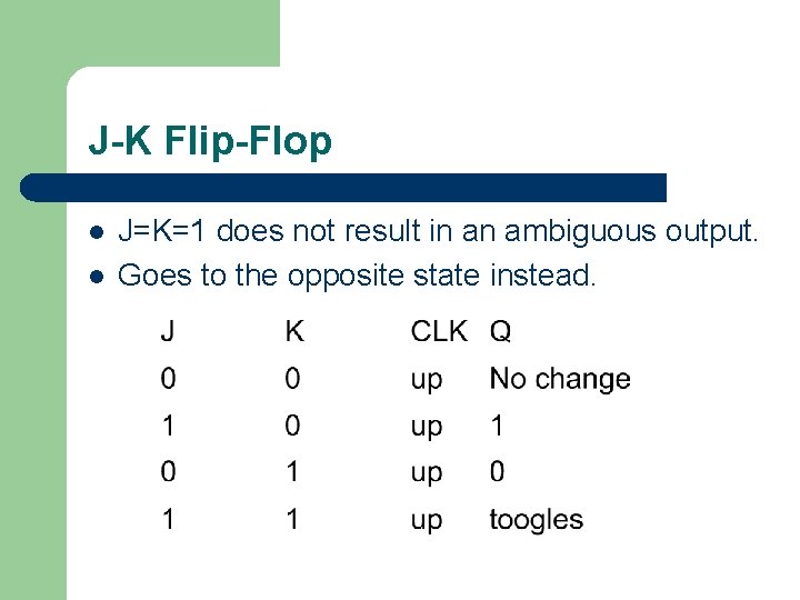
J-K Flip-Flop l l J=K=1 does not result in an ambiguous output. Goes to the opposite state instead.

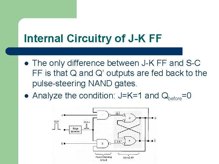
Internal Circuitry of J-K FF l l The only difference between J-K FF and S-C FF is that Q and Q’ outputs are fed back to the pulse-steering NAND gates. Analyze the condition: J=K=1 and Qbefore=0

Clocked D Flip-flop l l l Has only one control input D, which stands for data. Operation is simple: Q will go to the same state that is present on the D input when a PGT occurs at CLK. In other words, the level presented at D will be stored in the FF at the instant the PGT occurs.

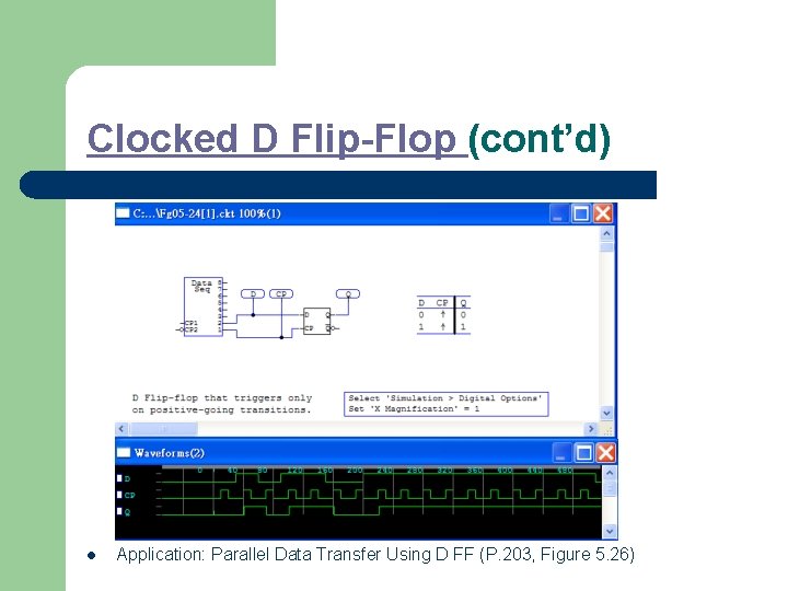
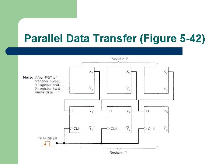
Clocked D Flip-Flop (cont’d) l Application: Parallel Data Transfer Using D FF (P. 203, Figure 5. 26)

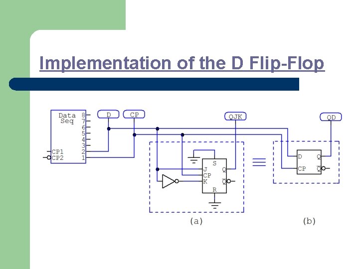
Implementation of the D Flip-Flop

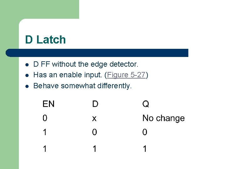
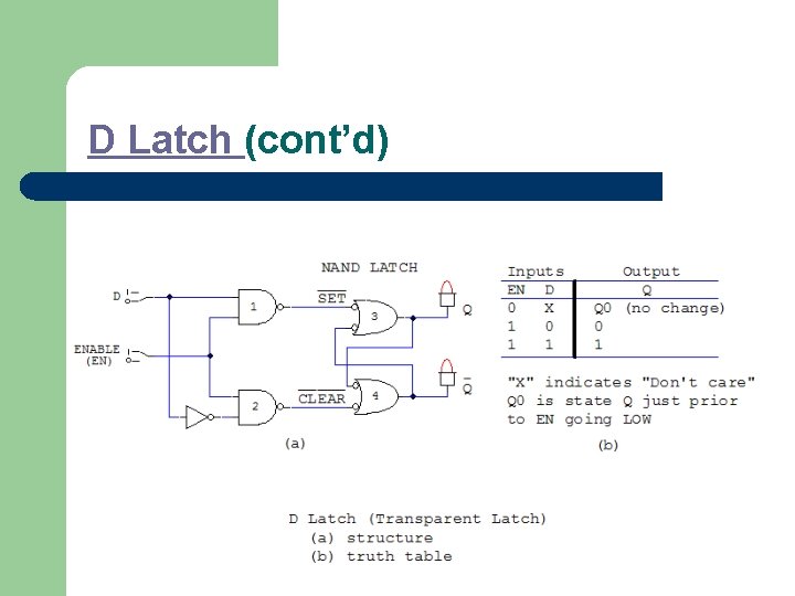
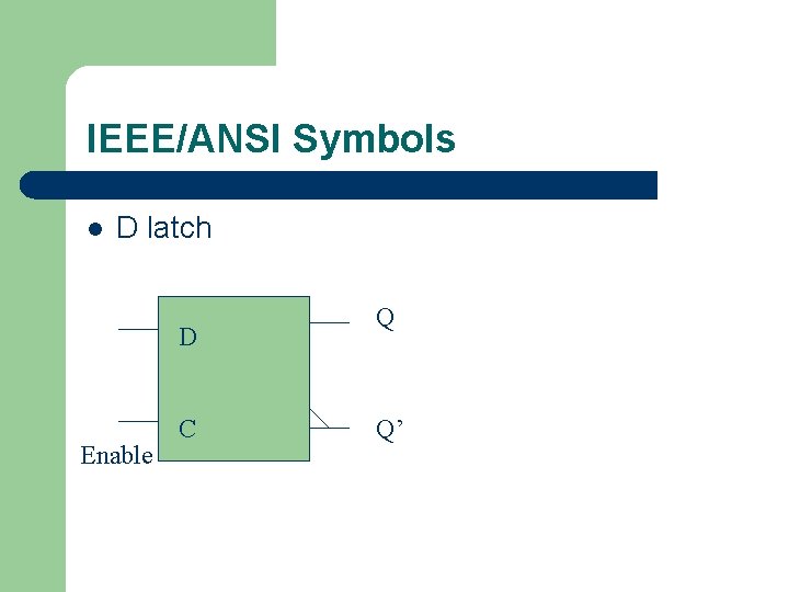
D Latch l l l D FF without the edge detector. Has an enable input. (Figure 5 -27) Behave somewhat differently.

D Latch (cont’d)

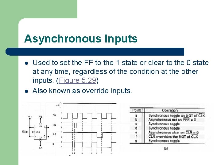
Asynchronous Inputs l l Used to set the FF to the 1 state or clear to the 0 state at any time, regardless of the condition at the other inputs. (Figure 5. 29) Also known as override inputs.

IEEE/ANSI Symbols l D latch D Enable C Q Q’

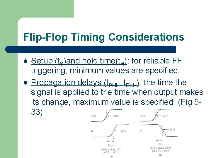
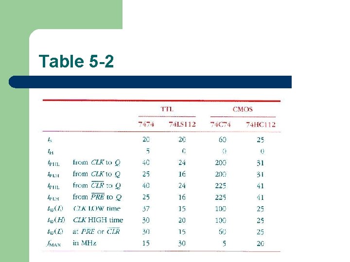
Flip-Flop Timing Considerations l l Setup (t. S)and hold time(t. H): for reliable FF triggering, minimum values are specified. Propagation delays (t. PHL, t. PLH): the time the signal is applied to the time when output makes its change, maximum value is specified. (Fig 533)

Timing Considerations (cont’d) l Maximum clocking frequency, f MAX: the highest frequency that can be applied to the CLK input of a FF and still have it trigger reliably.

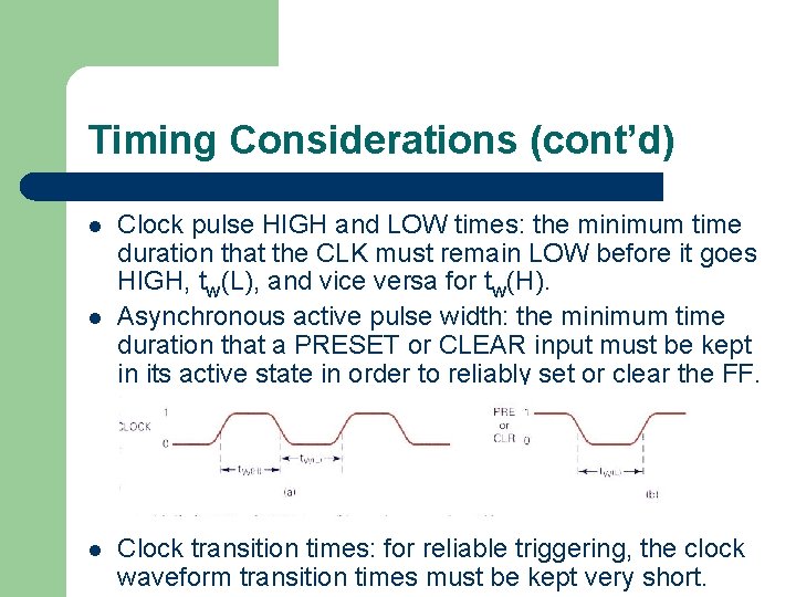
Timing Considerations (cont’d) l l l Clock pulse HIGH and LOW times: the minimum time duration that the CLK must remain LOW before it goes HIGH, tw(L), and vice versa for tw(H). Asynchronous active pulse width: the minimum time duration that a PRESET or CLEAR input must be kept in its active state in order to reliably set or clear the FF. Clock transition times: for reliable triggering, the clock waveform transition times must be kept very short.

Table 5 -2

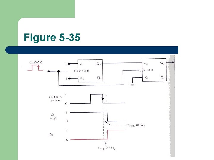
Potential Timing Problem l l l Refer to Figure 5 -35, problem can occur when output of one FF is connected to the input of another FF, and both FFs are triggered by the same clock signal. What if hold time requirement of Q 2 is greater than propagation delay of Q 1? Fortunately, all modern edge-triggered FFs have very short t. H, so there wouldn’t be a problem.

Figure 5 -35

Master/Slave Flip-Flops l l Used to solve the potential timing problem before the development of edge-triggered FFs with little or no hold-time requirement. Can be treated as a negative-edge-triggered FF.

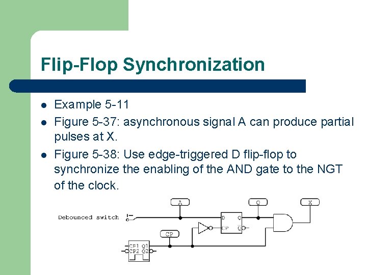
Flip-Flop Synchronization l l l Example 5 -11 Figure 5 -37: asynchronous signal A can produce partial pulses at X. Figure 5 -38: Use edge-triggered D flip-flop to synchronize the enabling of the AND gate to the NGT of the clock.

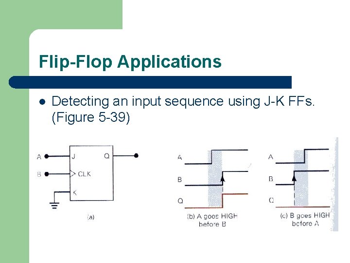
Flip-Flop Applications l Detecting an input sequence using J-K FFs. (Figure 5 -39)

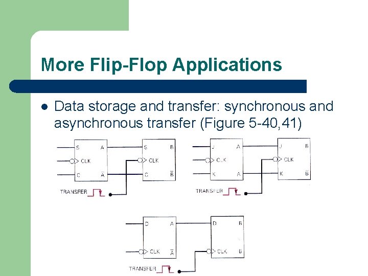
More Flip-Flop Applications l Data storage and transfer: synchronous and asynchronous transfer (Figure 5 -40, 41)

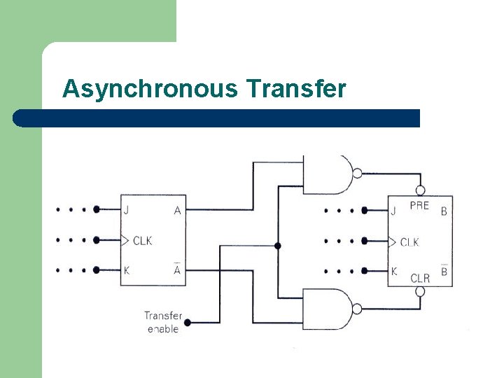
Asynchronous Transfer

Parallel Data Transfer (Figure 5 -42)

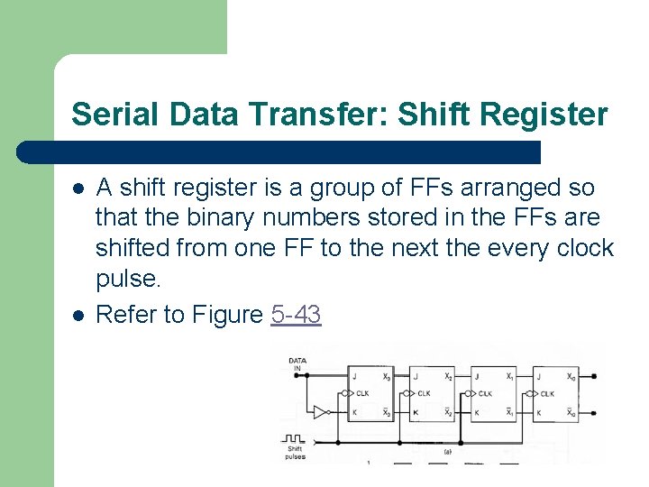
Serial Data Transfer: Shift Register l l A shift register is a group of FFs arranged so that the binary numbers stored in the FFs are shifted from one FF to the next the every clock pulse. Refer to Figure 5 -43

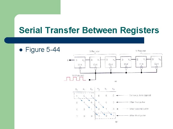
Serial Transfer Between Registers l Figure 5 -44

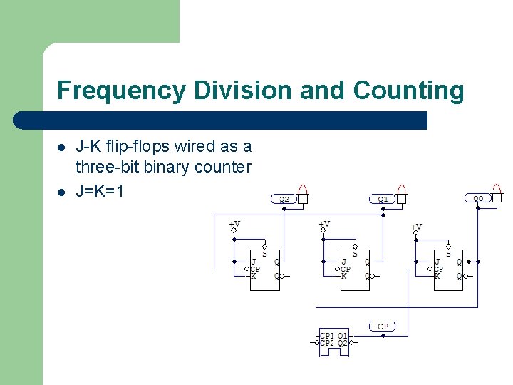
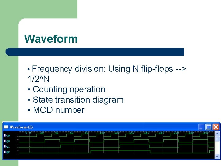
Frequency Division and Counting l l J-K flip-flops wired as a three-bit binary counter J=K=1

Waveform • Frequency division: Using N flip-flops --> 1/2^N • Counting operation • State transition diagram • MOD number

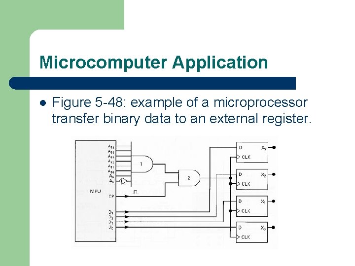
Microcomputer Application l Figure 5 -48: example of a microprocessor transfer binary data to an external register.

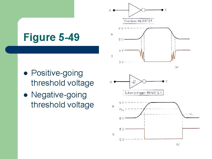
Schmitt-Trigger Devices l l A device that has a Schmitt-trigger type of input is designed to accept slow-changing signals and produce an output that has oscillation-free transitions. See Figure 5 -49, a Schmitt-trigger INVERTER

Figure 5 -49 l l Positive-going threshold voltage Negative-going threshold voltage

One-Shot l l Has only one stable output state (normally Q=0, Q’=1), also known as monostable multivibrator Once triggered, the output switches to the opposite state and remains in that ‘quasi-stable state’ for a fixed period of time, tp. Non-retriggerable OS Retriggerable OS

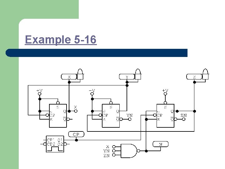
Analyzing Sequential Circuits l l Step 1: Examine the circuit. Look for familiar components. Step 2: Write down the logic levels present at each I/O prior to the occurrence of the first clock pulse. Step 3: Using the initial conditions to determine the new states of each FFs in response to the first clock pulse. Step 4: go back and repeat Steps 2, 3 for the 2 nd, 3 rd …clock pulse

Example 5 -16