Flip chip bump bonding needs at Diamond Light

Flip chip bump bonding needs at Diamond Light Source (Daresbury 15 th of May 2012) Presented by Nicola Tartoni

Outline 1. Hybrid detector technology in synchrotron research 2. The Excalibur development project at DLS 3. Bump bonding needs

Hybrid detector technology in synchrotron research

Hybrid detector technology in synchrotron research • Noiseless images • Fast read-out speed • No artefacts such as those due to phosphor afterglow • Expensive • Only silicon commercially available • Gaps between modules

EXCALIBUR Enhanced X-ray CAmera for Live Imaging and BURst mode operation Mode Counting Pixels 55 μm Read-out time 500 μs Sensor Silicon (300 μm) Area 11 cm x 10 cm (3 M pixels) ASIC MEDIPIX 3 Frame rate in continuous mode 100 images/s @ 12 bit ~0. 6 GBytes/s Frame rate in « Burst » mode 1000 images/s @ 12 bit ~ 6 GBytes/s vers RAM 10 cm DLS/STFC Development project
 8 x 2 MPX")
EXCALIBUR 3 modules 3 M pixels (11 x 10 cm) 8 x 2 MPX 3/module 1 FPGA card / row of 8 MPX 3 s Front-End Module (FEM) FPGA card Readout backend: 6 Linux nodes • Buffering, local storage & processing of image data • Interface to EPICS for DAQ & control
")
Mask of the 6’’ sensor wafers designed at Canberra (Belgium)

 with Sn/Pb solder")
Five EXCALIBUR hybrids produced Bonded at VTT (Finland) with Sn/Pb solder
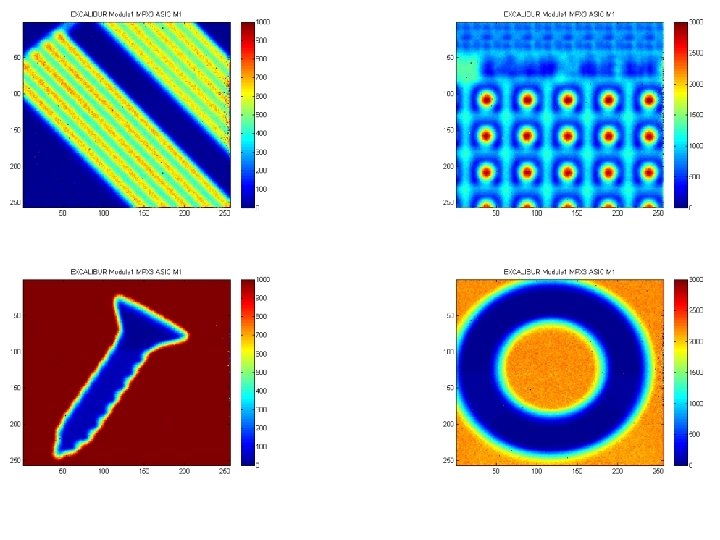
 Result of the test")
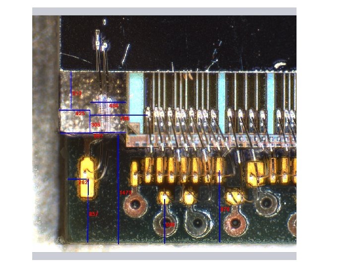
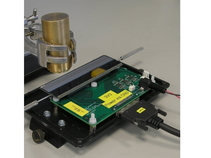
Probe station to test bare hybrids (Diamond detector group labs) Result of the test of the first hybrid: Probe card Connection to read-out Hybrid beneath • 16 ASICs bonded satisfactorily to the sensor with no obvious bonding issue • No hot spots detected • Overall 0. 9% bad pixels (not responding to Fe 55 X-rays and noisy pixels) • Better threshold equalization and higher energy X-rays might improve things

Jig to glue the base plate to the hybrids to the carrier electronic board for interconnections (Diamond detector group labs) Hybrid holder Alignment microscope Heating resistors First hybrid installed on the base plate with the ASICs wire-bonded to the carrier board (wire bonding STFC)

WISHES • 55 microns pitch indium bump bonding process availability: – Fluorescence background reduced – Applicable to materials such as Cd. Te • The quality of the process has to be very good and extremely well controlled • Processing of sensors has to be available routinely for “mass” production

Solution: indium bump bonding at RAL • Investment in a bump bonding process development project (equipment, staff, money) • Training of permanent staff to guarantee the quality and the production capacity
- Slides: 16