Flash storage COS 518 Advanced Computer Systems Lecture
- Slides: 19

Flash storage COS 518: Advanced Computer Systems Lecture 9 Michael Freedman

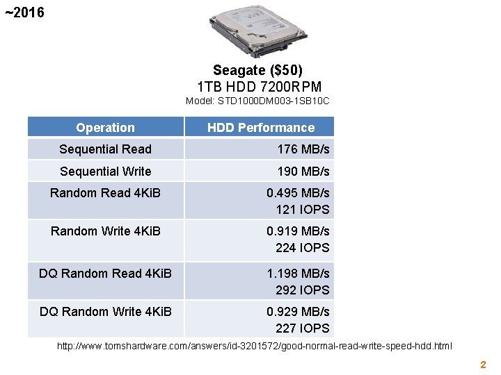
~2016 Seagate ($50) 1 TB HDD 7200 RPM Model: STD 1000 DM 003 -1 SB 10 C Operation HDD Performance Sequential Read 176 MB/s Sequential Write 190 MB/s Random Read 4 Ki. B 0. 495 MB/s 121 IOPS Random Write 4 Ki. B 0. 919 MB/s 224 IOPS DQ Random Read 4 Ki. B 1. 198 MB/s 292 IOPS DQ Random Write 4 Ki. B 0. 929 MB/s 227 IOPS http: //www. tomshardware. com/answers/id-3201572/good-normal-read-write-speed-hdd. html 2

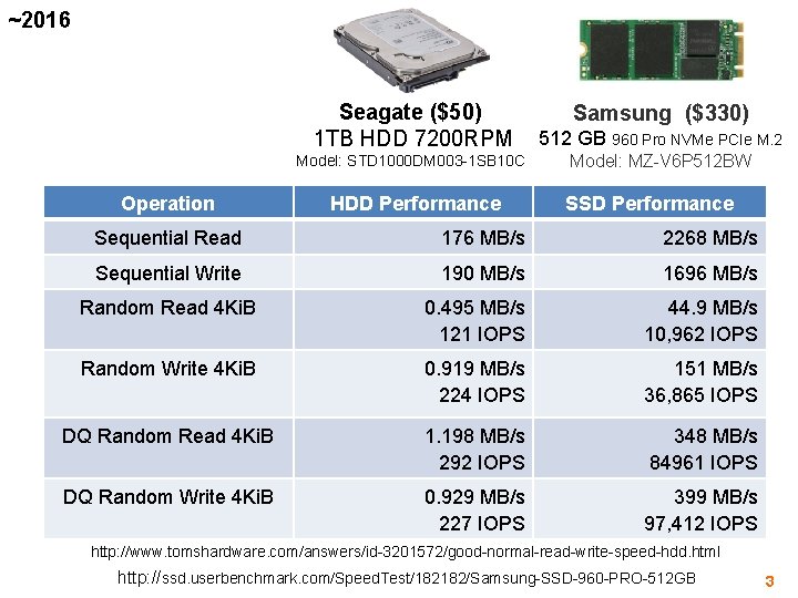
~2016 Operation Seagate ($50) 1 TB HDD 7200 RPM 512 GB 960 Pro NVMe PCIe M. 2 Model: STD 1000 DM 003 -1 SB 10 C Model: MZ-V 6 P 512 BW HDD Performance Samsung ($330) SSD Performance Sequential Read 176 MB/s 2268 MB/s Sequential Write 190 MB/s 1696 MB/s Random Read 4 Ki. B 0. 495 MB/s 121 IOPS 44. 9 MB/s 10, 962 IOPS Random Write 4 Ki. B 0. 919 MB/s 224 IOPS 151 MB/s 36, 865 IOPS DQ Random Read 4 Ki. B 1. 198 MB/s 292 IOPS 348 MB/s 84961 IOPS DQ Random Write 4 Ki. B 0. 929 MB/s 227 IOPS 399 MB/s 97, 412 IOPS http: //www. tomshardware. com/answers/id-3201572/good-normal-read-write-speed-hdd. html http: //ssd. userbenchmark. com/Speed. Test/182182/Samsung-SSD-960 -PRO-512 GB 3

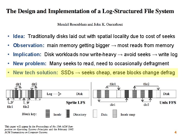
• Idea: Traditionally disks laid out with spatial locality due to cost of seeks • Observation: main memory getting bigger → most reads from memory • Implication: Disk workloads now write-heavy → avoid seeks → write log • New problem: Many seeks to read, need to occasionally defragment • New tech solution: SSDs → seeks cheap, erase blocks change defrag 4

Flash: Storing individual bits 5

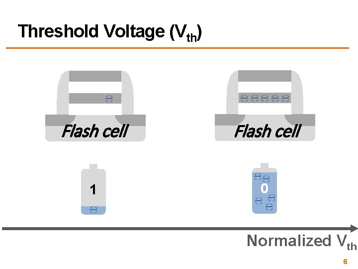
Threshold Voltage (Vth) Flash cell 1 0 Normalized Vth 6

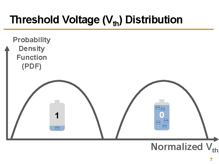
Threshold Voltage (Vth) Distribution Probability Density Function (PDF) 1 0 Normalized Vth 7

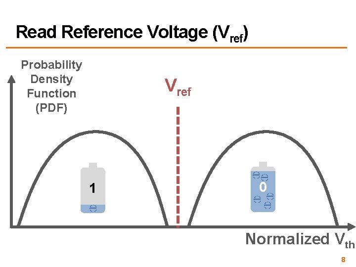
Read Reference Voltage (Vref) Probability Density Function (PDF) Vref 1 0 Normalized Vth 8

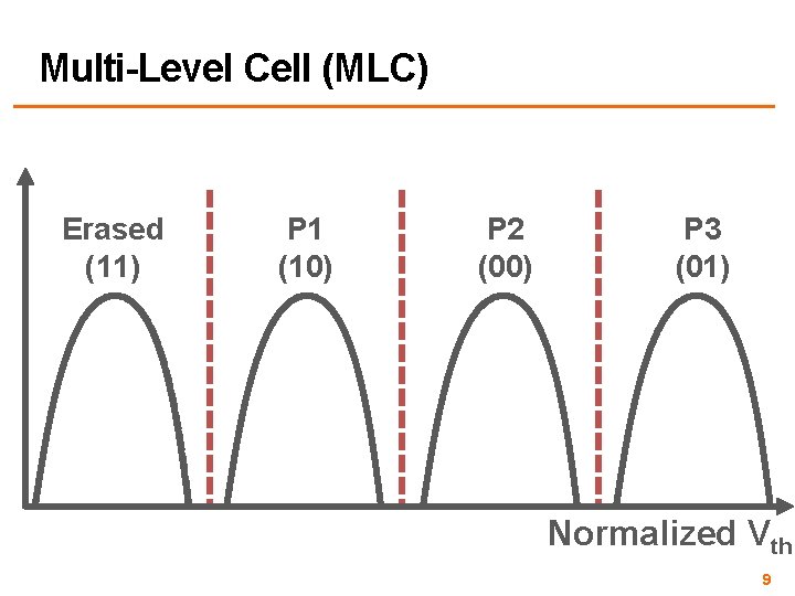
Multi-Level Cell (MLC) Erased (11) P 1 (10) P 2 (00) P 3 (01) Normalized Vth 9

Flash: Storing many bits 10

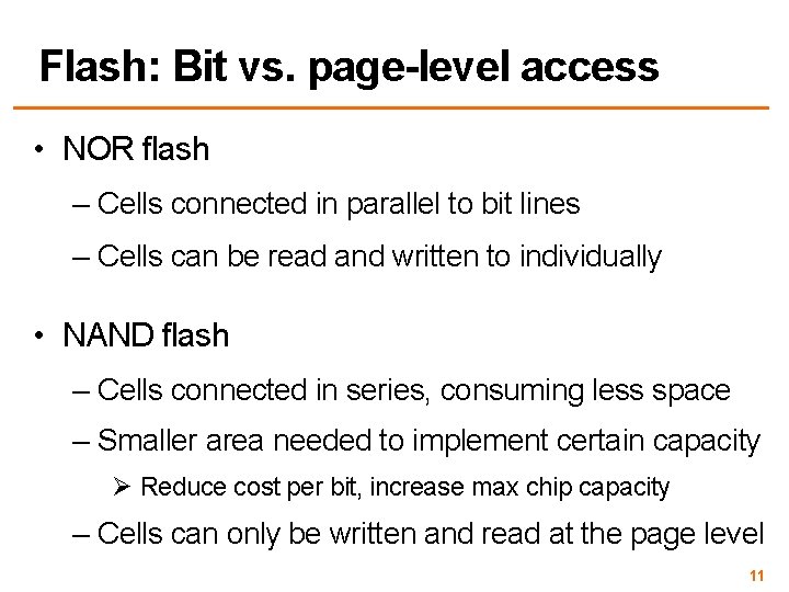
Flash: Bit vs. page-level access • NOR flash – Cells connected in parallel to bit lines – Cells can be read and written to individually • NAND flash – Cells connected in series, consuming less space – Smaller area needed to implement certain capacity Ø Reduce cost per bit, increase max chip capacity – Cells can only be written and read at the page level 11

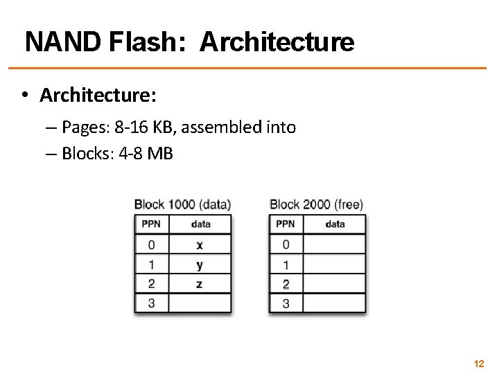
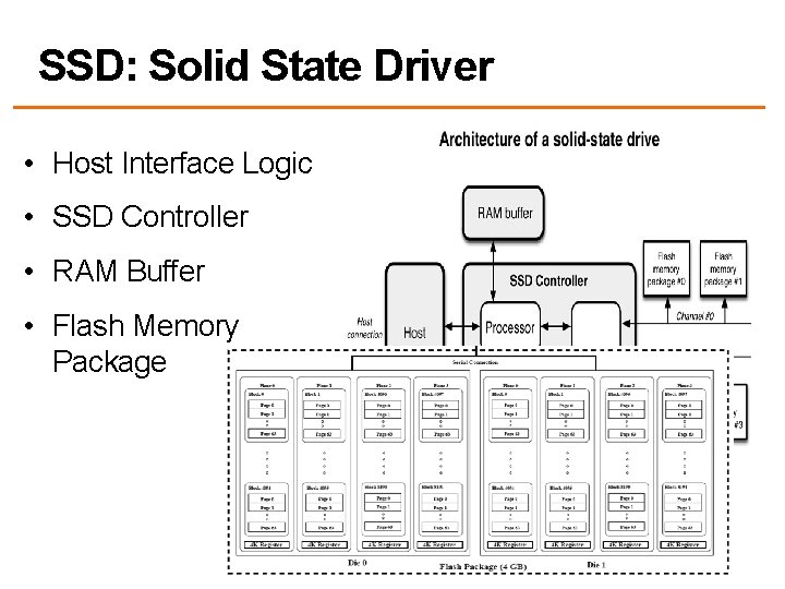
NAND Flash: Architecture • Architecture: – Pages: 8 -16 KB, assembled into – Blocks: 4 -8 MB 12

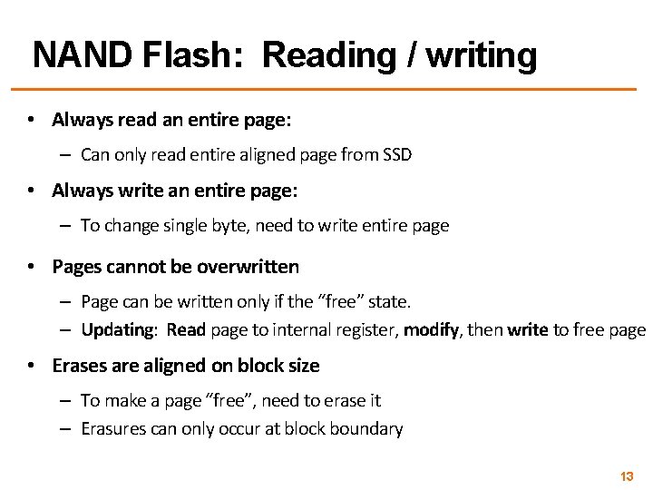
NAND Flash: Reading / writing • Always read an entire page: – Can only read entire aligned page from SSD • Always write an entire page: – To change single byte, need to write entire page • Pages cannot be overwritten – Page can be written only if the “free” state. – Updating: Read page to internal register, modify, then write to free page • Erases are aligned on block size – To make a page “free”, need to erase it – Erasures can only occur at block boundary 13

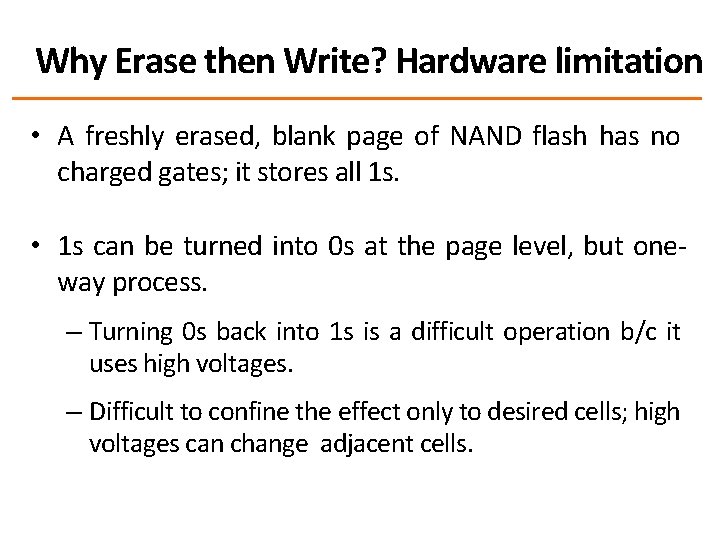
Why Erase then Write? Hardware limitation • A freshly erased, blank page of NAND flash has no charged gates; it stores all 1 s. • 1 s can be turned into 0 s at the page level, but oneway process. – Turning 0 s back into 1 s is a difficult operation b/c it uses high voltages. – Difficult to confine the effect only to desired cells; high voltages can change adjacent cells.

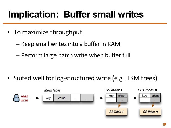
Implication: Buffer small writes • To maximize throughput: – Keep small writes into a buffer in RAM – Perform large batch write when buffer full • Suited well for log-structured write (e. g. , LSM trees) 15

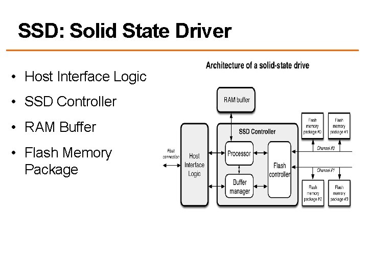
SSD architecture 16

SSD: Solid State Driver • Host Interface Logic • SSD Controller • RAM Buffer • Flash Memory Package

SSD: Solid State Driver • Host Interface Logic • SSD Controller • RAM Buffer • Flash Memory Package

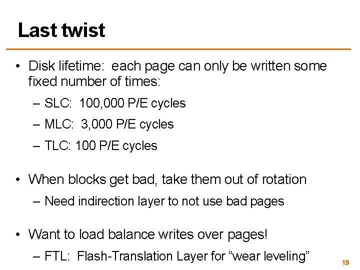
Last twist • Disk lifetime: each page can only be written some fixed number of times: – SLC: 100, 000 P/E cycles – MLC: 3, 000 P/E cycles – TLC: 100 P/E cycles • When blocks get bad, take them out of rotation – Need indirection layer to not use bad pages • Want to load balance writes over pages! – FTL: Flash-Translation Layer for “wear leveling” 19