Flash Memory Computer Science Engineering Department Arizona State

- Slides: 9

Flash Memory Computer Science & Engineering Department Arizona State University Tempe, AZ 85287 Dr. Yann-Hang Lee yhlee@asu. edu (480) 727 -7507 7/23

Flash Memory q A type of EEPROM (Electrically-Erasable programmable Read-Only Memory) v an older type of memory that used UV-light to erase q Non-volatile, solid state technology q Relatively limited lifespan q Information is stored in an array of memory cells made from floating-gate (FG) transistors q Packaged inside a memory card: v Extremely durable v Can withstand intense pressure v Immersion in water q Better kinetic shock resistance than hard disks set 4 -- 1

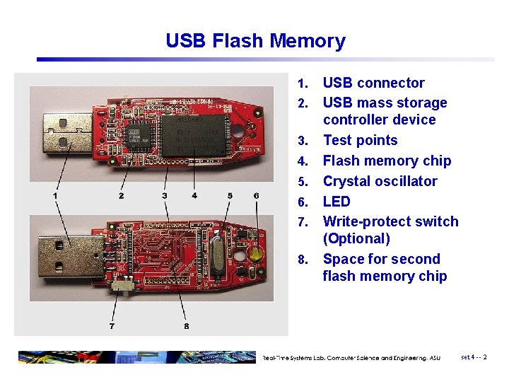
USB Flash Memory 1. 2. 3. 4. 5. 6. 7. 8. USB connector USB mass storage controller device Test points Flash memory chip Crystal oscillator LED Write-protect switch (Optional) Space for second flash memory chip set 4 -- 2

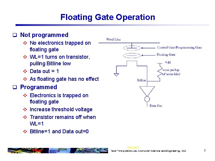
Floating Gate Operation q Not programmed v No electronics trapped on floating gate v WL=1 turns on transistor, pulling Bitline low v Data out = 1 v As floating gate has no effect q Programmed v Electronics is trapped on floating gate v Increase threshold voltage v Transistor remains off when WL=1 v Bitline=1 and Data out=0 Sept 2007 3

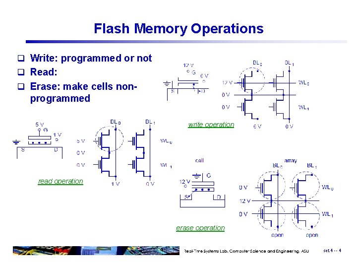
Flash Memory Operations q Write: programmed or not q Read: q Erase: make cells non- programmed write operation read operation erase operation set 4 -- 4

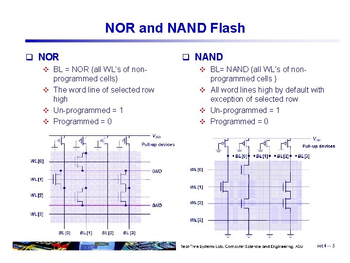
NOR and NAND Flash q NOR q NAND v BL = NOR (all WL’s of non- v BL= NAND (all WL’s of non- programmed cells) v The word line of selected row high v Un-programmed = 1 v Programmed = 0 programmed cells ) v All word lines high by default with exception of selected row v Un-programmed = 1 v Programmed = 0 set 4 -- 5

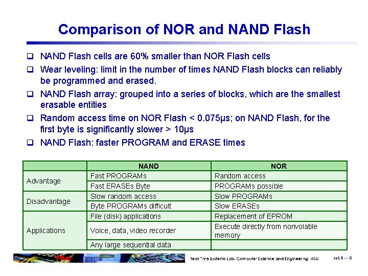
Comparison of NOR and NAND Flash q NAND Flash cells are 60% smaller than NOR Flash cells q Wear leveling: limit in the number of times NAND Flash blocks can reliably be programmed and erased. q NAND Flash array: grouped into a series of blocks, which are the smallest erasable entities q Random access time on NOR Flash < 0. 075μs; on NAND Flash, for the first byte is significantly slower > 10μs q NAND Flash: faster PROGRAM and ERASE times Advantage Disadvantage Applications NAND Fast PROGRAMs Fast ERASEs Byte Slow random access Byte PROGRAMs difficult File (disk) applications Voice, data, video recorder NOR Random access PROGRAMs possible Slow PROGRAMs Slow ERASEs Replacement of EPROM Execute directly from nonvolatile memory Any large sequential data set 4 -- 6

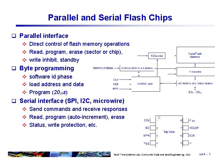
Parallel and Serial Flash Chips q Parallel interface v Direct control of flash memory operations v Read, program, erase (sector or chip), v write inhibit, standby q Byte programming v software id phase v load address and data v Program (20 s) q Serial interface (SPI, I 2 C, microwire) v Send commands and receive responses v Read, program (auto-increment), erase v Status, write protection, etc. set 4 -- 7

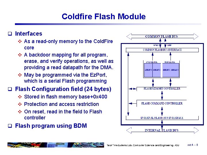
Coldfire Flash Module q Interfaces v As a read-only memory to the Cold. Fire core v A backdoor mapping for all program, erase, and verify operations, as well as providing a read datapath for the DMA. v May be programmed via the Ez. Port, which is a serial Flash programming q Flash Configuration field (24 bytes) v Stored in flash memory base+0 x 400 v Protection and access restriction v On reset, read in the field to Flash controller q Flash program using BDM set 4 -- 8