Fixed Bias Amplifier Circuit Using BJT Presented by

Fixed Bias Amplifier Circuit Using BJT Presented by Mrs. Shifana Parween. A

AIM To design and construct BJT Common Emitter Amplifier using fixed bias. To measure the gain and to plot the frequency response and to determine the Gain Bandwidth.
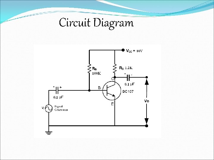
Circuit Diagram
applications Fixed bias is rarely used in linear circuits in which the transistor is used as a current source. It is often used in circuits where transistor is used as a switch. Fixed bias is used to achieve crude automatic gain control in the transistor by feeding the base resistor from a DC signal derived from the AC output of a later stage.
NEED FOR BIASING The supply voltages and resistances must be properly chosen in order to produce distortion less output. These voltages and resistances establish a set of DC voltage VCEQ and the current ICQ to operate the transistor in the active region. They are called the Quiesent values which determine the operating point of the circuit.

FIXED BIAS A high resistance R B is connected between Vcc and the base of the transistor. This helps in keeping the operating point in the active region. By proper selection of RB required zero signal base current can be achieved. Also called as base biasing.
FREQUENCY RESPONSE OF CE AMPLIFIER Frequency response is a plot between the Gain factor (AV) in d. B and the frequency in Hz. The main purpose is to determine the frequency response of amplifier circuits due to the circuit capacitors and transistor capacitances. It is used to determine the bandwidth of the circuit.
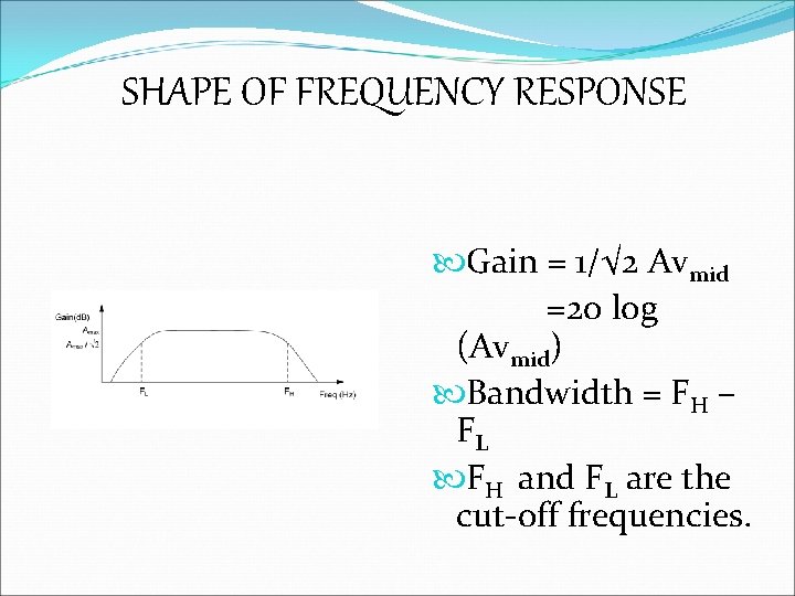
SHAPE OF FREQUENCY RESPONSE Gain = 1/√ 2 Avmid =20 log (Avmid) Bandwidth = FH – FL FH and FL are the cut-off frequencies.
REASON FOR THE DROP AT CUT-OFF REGION It consist of three regions. a) Low frequency region. b) Mid frequency region c) High frequency region At low frequency region the drop is due to the increase in the Capacitive reactances. At the high frequency region the drop is due to the parasitic capacitances or the frequency dependence of the networks gain on the active devices.
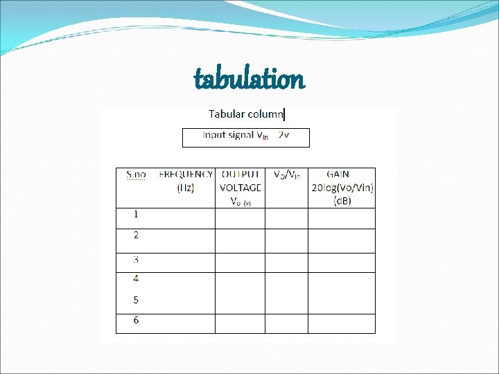
tabulation
Procedure Connect the circuit as per the circuit diagram Set Vin using the signal generator. Keeping input voltage constant, vary the frequency from 1 Hz to 1 MHz in regular steps. Note down the corresponding output voltage. Plot the graph: Gain in d. B Vs Frequency in Hz. Calculate the Bandwidth from the Frequency response graph.
plot the Frequency Response The frequency response curve is plotted on a semilog scale. The mid frequency voltage gain is divided by √ 2 and these points are marked in the frequency response curve. The high frequency point is called the upper 3 d. B point. The lower frequency point is called the lower 3 d. B point. The difference between the upper 3 d. B point and the lower 3 d. B point in the frequency scale gives the bandwidth of the amplifier. From the plotted graph the bandwidth is obtained. (i. e) Bandwidth = f. H - f. L
Merits and Demerits Merits: The circuit has the tendency As β value is fixed for a given transistor, this relation can to stabilize operating point be satisfied either by keeping against changes in RE very large, or making RB temperature and value. very low. Demerits: If RE is of large value, high In this circuit, to keep IC VCC is necessary. This independent of the following increases cost as well as condition must be met precautions necessary while handling
- Slides: 13