First Results from Cherwell a CMOS sensor for
- Slides: 15

First Results from Cherwell, a CMOS sensor for Particle Physics By James Mylroie-Smith https: //heplnm 061. pp. rl. ac. uk/display/arachnid/Home

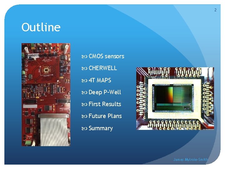
2 Outline CMOS sensors CHERWELL 4 T MAPS Deep P-Well First Results Future Plans Summary James Mylroie-Smith

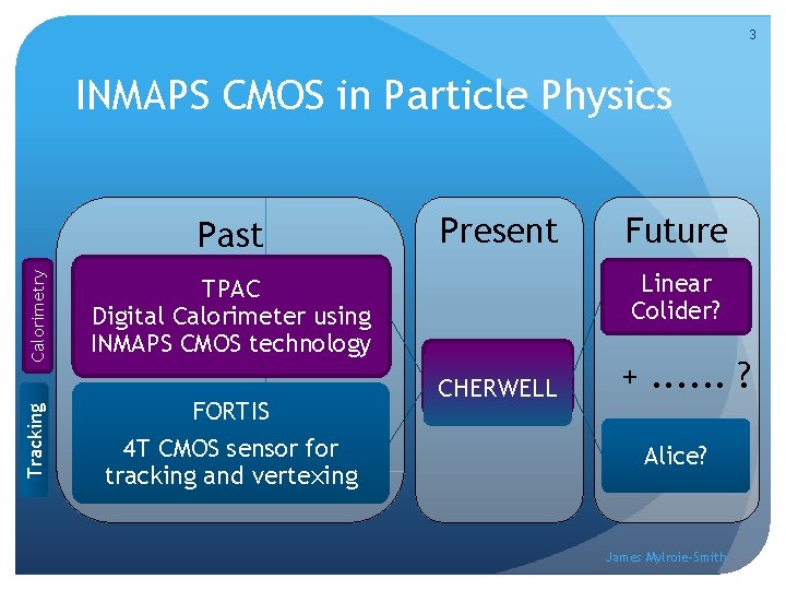
3 INMAPS CMOS in Particle Physics Tracking Calorimetry Past Present Linear Colider? TPAC Digital Calorimeter using INMAPS CMOS technology FORTIS 4 T CMOS sensor for tracking and vertexing Future CHERWELL +. . . ? Alice? James Mylroie-Smith

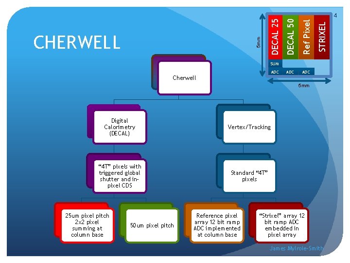
Ref Pixel ADC STRIXEL DECAL 50 DECAL 25 5 mm CHERWELL 4 SUM ADC Cherwell 5 mm Digital Calorimetry (DECAL) Vertex/Tracking “ 4 T” pixels with triggered global shutter and inpixel CDS Standard “ 4 T” pixels 25 um pixel pitch 2 x 2 pixel summing at column base 50 um pixel pitch Reference pixel array 12 bit ramp ADC implemented at column base “Strixel” array 12 bit ramp ADC embedded in pixel array James Mylroie-Smith

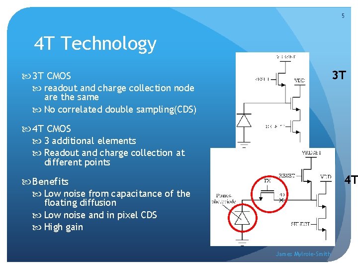
5 4 T Technology 3 T CMOS readout and charge collection node are the same No correlated double sampling(CDS) 4 T CMOS 3 additional elements Readout and charge collection at different points 4 T Benefits Low noise from capacitance of the floating diffusion Low noise and in pixel CDS High gain James Mylroie-Smith

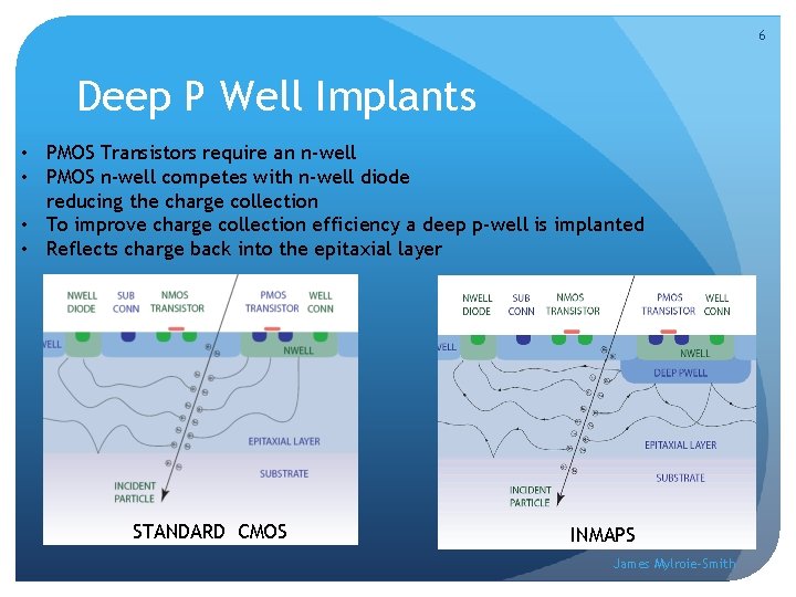
6 Deep P Well Implants • PMOS Transistors require an n-well • PMOS n-well competes with n-well diode reducing the charge collection • To improve charge collection efficiency a deep p-well is implanted • Reflects charge back into the epitaxial layer STANDARD CMOS INMAPS James Mylroie-Smith

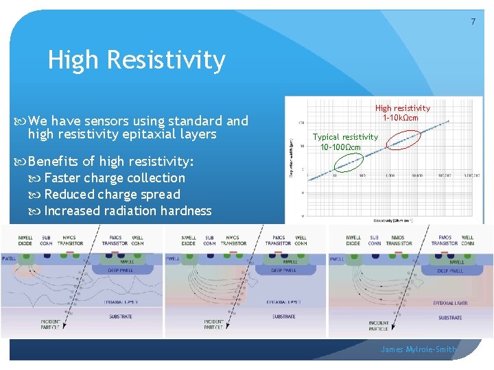
7 High Resistivity We have sensors using standard and high resistivity epitaxial layers High resistivity 1 -10 kΩcm Typical resistivity 10 -100Ωcm Benefits of high resistivity: Faster charge collection Reduced charge spread Increased radiation hardness James Mylroie-Smith

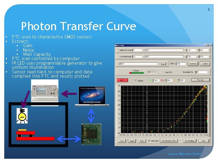
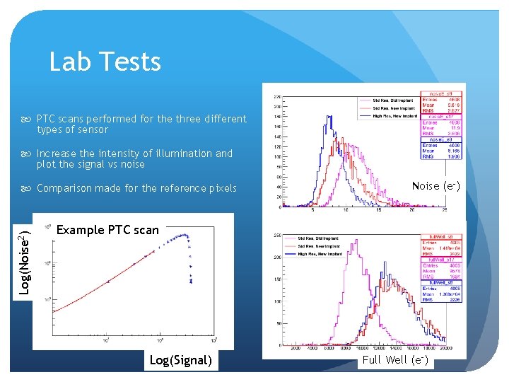
8 Photon Transfer Curve • • • PTC used to characterise CMOS censors Extract: • Gain • Noise • Well Capacity PTC scan controlled by computer IR LED uses programmable generator to give uniform illumination Sensor read back to computer and data complied into PTC and results plotted James Mylroie-Smith

Lab Tests PTC scans performed for the three different types of sensor Increase the intensity of illumination and plot the signal vs noise Log(Noise 2) Comparison made for the reference pixels Noise (e-) Example PTC scan Log(Signal) Full Well (e-)

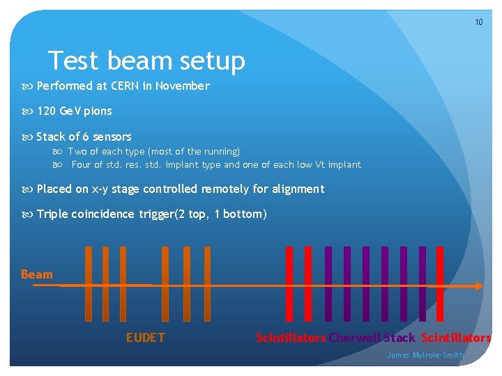
10 Test beam setup Performed at CERN in November 120 Ge. V pions Stack of 6 sensors Two of each type (most of the running) Four of std. res. std. implant type and one of each low Vt implant Placed on x-y stage controlled remotely for alignment Triple coincidence trigger(2 top, 1 bottom) Beam EUDET Scintillators Cherwell Stack Scintillators James Mylroie-Smith

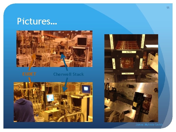
11 Pictures… EUDET Cherwell Stack James Mylroie-Smith

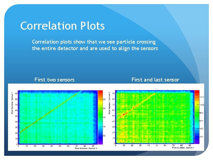
Correlation Plots Correlation plots show that we see particle crossing the entire detector and are used to align the sensors First two sensors First and last sensor

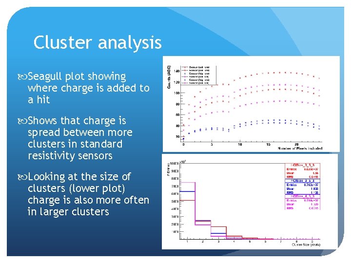
Cluster analysis Seagull plot showing where charge is added to a hit Shows that charge is spread between more clusters in standard resistivity sensors Looking at the size of clusters (lower plot) charge is also more often in larger clusters

Future Plans Cherwell 2 has been designed for possible use in ALICE Chip is now being fabricated (paid for by CERN) One of three designs for the ALICE upgrade Due back in 2 months Plans to test DECAL at DESY test beam in June

Summary Cherwell sensor is performing well A range of tests have been performed to compare different sensor types. And understand their performance. Test beam results are being understood.