Finite State Machine FSM q When the sequence
- Slides: 22

Finite State Machine (FSM) q When the sequence of actions in your design depend on the state of sequential elements, a finite state machine (FSM) can be implemented q FSMs are widely used in applications that require prescribed sequential activity Ø Example: • • • Sequence Detector Fancy counters Traffic Light Controller Data-path Controller Device Interface Controller etc.

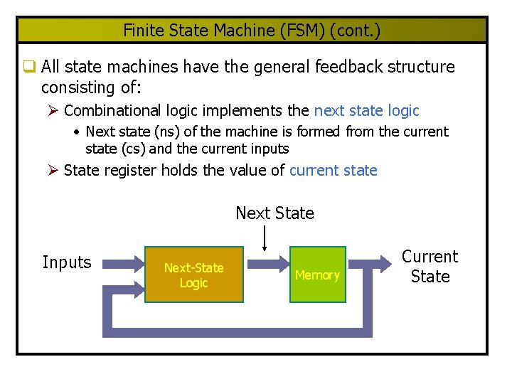
Finite State Machine (FSM) (cont. ) q All state machines have the general feedback structure consisting of: Ø Combinational logic implements the next state logic • Next state (ns) of the machine is formed from the current state (cs) and the current inputs Ø State register holds the value of current state Next State Inputs Next-State Logic Memory Current State

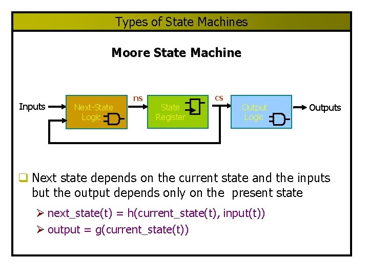
Types of State Machines Moore State Machine Inputs Next-State Logic ns cs State Register Output Logic Outputs q Next state depends on the current state and the inputs but the output depends only on the present state Ø next_state(t) = h(current_state(t), input(t)) Ø output = g(current_state(t))

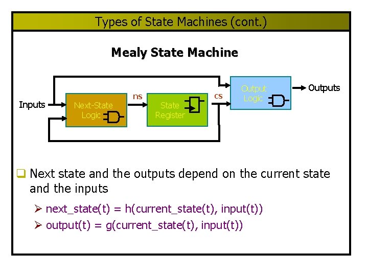
Types of State Machines (cont. ) Mealy State Machine Inputs Next-State Logic ns cs State Register Output Logic Outputs q Next state and the outputs depend on the current state and the inputs Ø next_state(t) = h(current_state(t), input(t)) Ø output(t) = g(current_state(t), input(t))

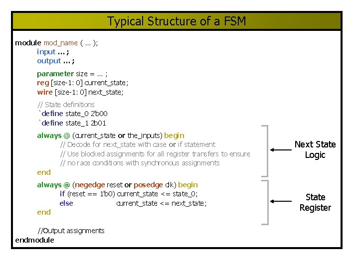
Typical Structure of a FSM module mod_name ( … ); input … ; output … ; parameter size = … ; reg [size-1: 0] current_state; wire [size-1: 0] next_state; // State definitions `define state_0 2'b 00 `define state_1 2 b 01 always @ (current_state or the_inputs) begin // Decode for next_state with case or if statement // Use blocked assignments for all register transfers to ensure // no race conditions with synchronous assignments end always @ (negedge reset or posedge clk) begin if (reset == 1'b 0) current_state <= state_0; else current_state <= next_state; end //Output assignments endmodule Next State Logic State Register

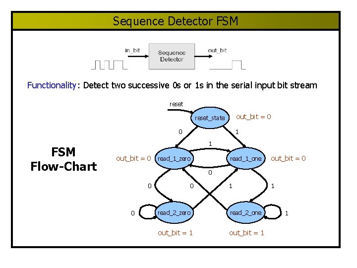
Sequence Detector FSM Functionality: Detect two successive 0 s or 1 s in the serial input bit stream reset out_bit = 0 reset_state 0 FSM Flow-Chart 1 1 out_bit = 0 read_1_zero read_1_one out_bit = 0 1 1 0 0 read_2_zero read_2_one out_bit = 1 1

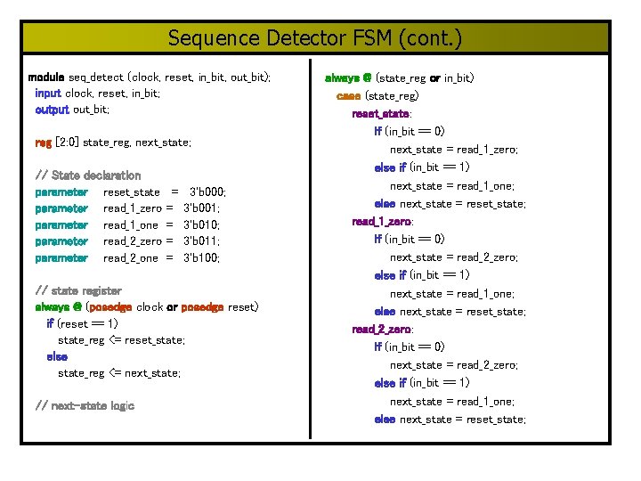
Sequence Detector FSM (cont. ) module seq_detect (clock, reset, in_bit, out_bit); input clock, reset, in_bit; output out_bit; reg [2: 0] state_reg, next_state; // State declaration parameter reset_state parameter read_1_zero parameter read_1_one parameter read_2_zero parameter read_2_one = = = 3'b 000; 3'b 001; 3'b 010; 3'b 011; 3'b 100; // state register always @ (posedge clock or posedge reset) if (reset == 1) state_reg <= reset_state; else state_reg <= next_state; // next-state logic always @ (state_reg or in_bit) case (state_reg) reset_state: if (in_bit == 0) next_state = read_1_zero; else if (in_bit == 1) next_state = read_1_one; else next_state = reset_state; read_1_zero: if (in_bit == 0) next_state = read_2_zero; else if (in_bit == 1) next_state = read_1_one; else next_state = reset_state; read_2_zero: if (in_bit == 0) next_state = read_2_zero; else if (in_bit == 1) next_state = read_1_one; else next_state = reset_state;

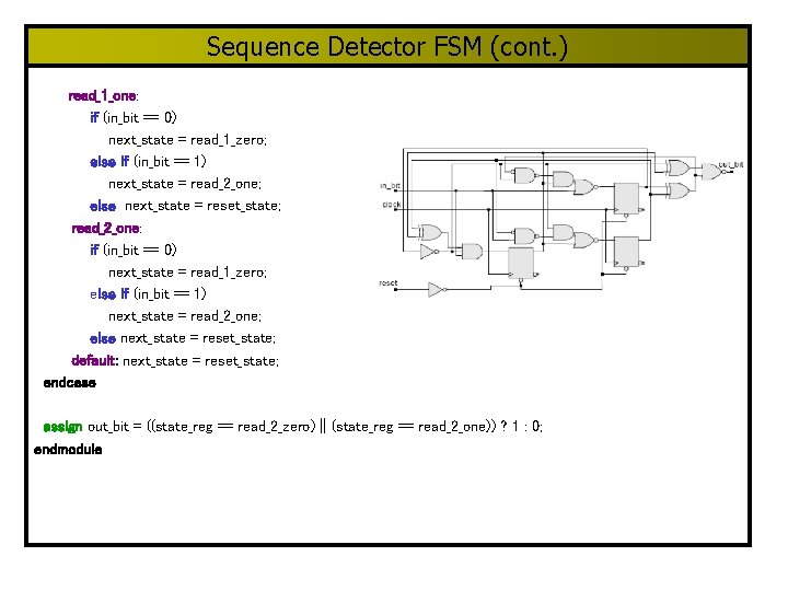
Sequence Detector FSM (cont. ) read_1_one: if (in_bit == 0) next_state = read_1_zero; else if (in_bit == 1) next_state = read_2_one; else next_state = reset_state; read_2_one: if (in_bit == 0) next_state = read_1_zero; else if (in_bit == 1) next_state = read_2_one; else next_state = reset_state; default: next_state = reset_state; endcase assign out_bit = ((state_reg == read_2_zero) || (state_reg == read_2_one)) ? 1 : 0; endmodule

Clock Domain Synchronization q Larger designs generally consists of several parts that operate at independent clocks – clock domains q Clock domain synchronization is required when ever a signal traverses from one clock domain to another clock domain q Problem can be treated as the case where flip-flop data input is asynchronous Ø Can cause metastabilty in the receiving flip-flop Ø Rupture the sequential behavior q This can be avoided by using synchronization circuits

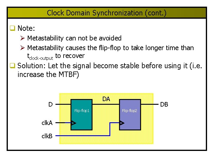
Clock Domain Synchronization (cont. ) q Note: Ø Metastability can not be avoided Ø Metastability causes the flip-flop to take longer time than tclock-output to recover q Solution: Let the signal become stable before using it (i. e. increase the MTBF) DA D Flip-flop 1 clk. A clk. B DB Flip-flop 2

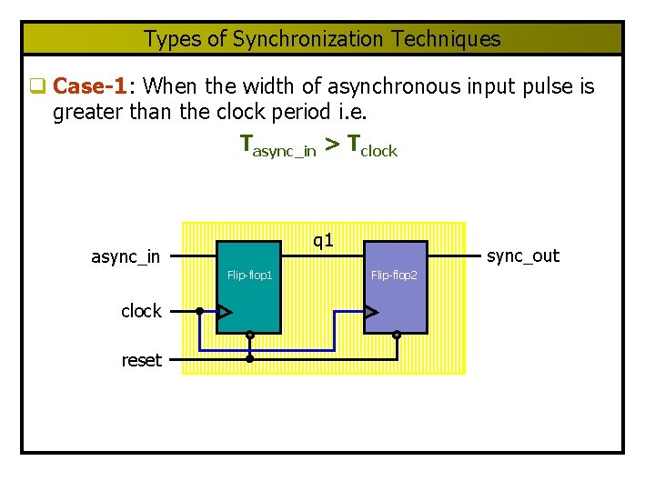
Types of Synchronization Techniques q Case-1: When the width of asynchronous input pulse is greater than the clock period i. e. Tasync_in > Tclock q 1 async_in Flip-flop 1 clock reset sync_out Flip-flop 2

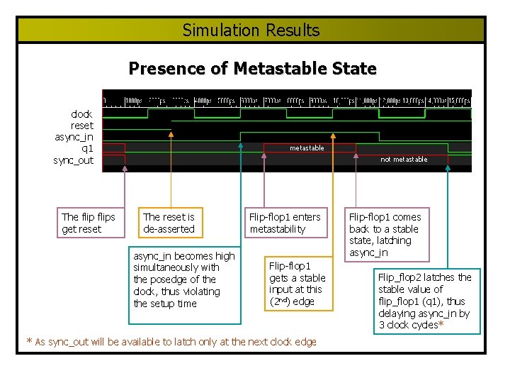
Simulation Results Presence of Metastable State clock reset async_in q 1 sync_out The flips get reset metastable not metastable The reset is de-asserted async_in becomes high simultaneously with the posedge of the clock, thus violating the setup time Flip-flop 1 enters metastability Flip-flop 1 gets a stable input at this (2 nd) edge * As sync_out will be available to latch only at the next clock edge Flip-flop 1 comes back to a stable state, latching async_in Flip_flop 2 latches the stable value of flip_flop 1 (q 1), thus delaying async_in by 3 clock cycles*

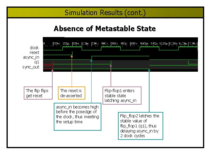
Simulation Results (cont. ) Absence of Metastable State clock reset async_in q 1 sync_out The flips get reset The reset is de-asserted async_in becomes high before the posedge of the clock, thus meeting the setup time Flip-flop 1 enters stable state latching async_in Flip_flop 2 latches the stable value of flip_flop 1 (q 1), thus delaying async_in by 2 clock cycles

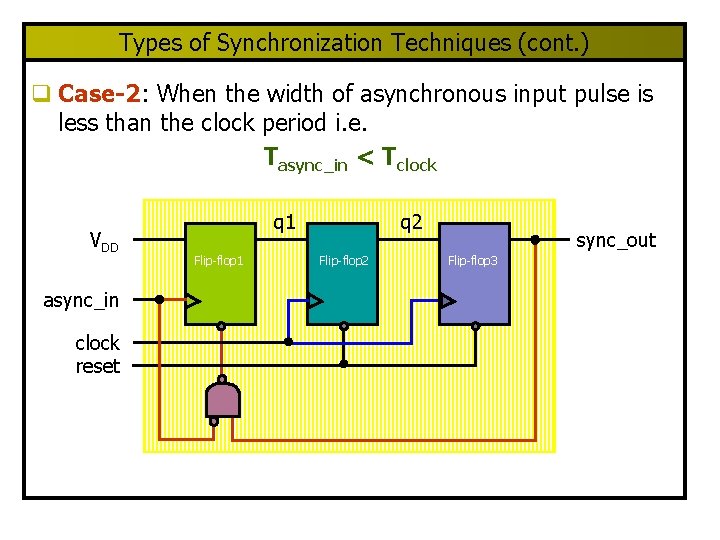
Types of Synchronization Techniques (cont. ) q Case-2: When the width of asynchronous input pulse is less than the clock period i. e. Tasync_in < Tclock VDD async_in clock reset q 1 Flip-flop 1 q 2 Flip-flop 2 sync_out Flip-flop 3

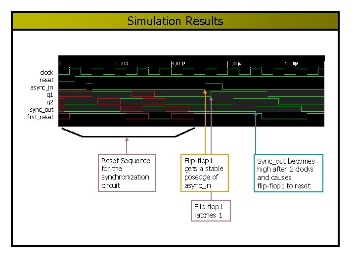
Simulation Results clock reset async_in q 1 q 2 sync_out first_reset Reset Sequence for the synchronization circuit Flip-flop 1 gets a stable posedge of async_in Flip-flop 1 latches 1 Sync_out becomes high after 2 clocks and causes flip-flop 1 to reset

First-in First-out Memory (FIFO) q When the source clock is higher than the destination clock, loss of data can occur due to inability of the destination to sample at the source speed q How to avoid this? Ø Use handshake signals (i. e. supply data only when the destination is ready to receive e. g. master-slave protocol) • Transfer rates are lower Ø High performance parallel interfaces between independent clock domains are implemented with first-in first-out memory called FIFO.

FIFO Features q A FIFO consists of block of memory and a controller that manages the traffic of data to and from the FIFO q A FIFO provides access to only one register cell at a time (not the entire array of registers) q A FIFO has two address pointers, one for writing to the next available cell, and another one for reading the next unread cell q The pointers for reading and writing are relocated dynamically as commands to read or write are received q A pointer is moved after each operation q A FIFO can receive data until it is full and can be read until it is empty

FIFO Features (cont. ) q A FIFO has: Ø Separate address pointers and datapaths for reading and writing data Ø Status lines indicating the condition of the stack (full, almost full, empty etc. ) q The input (write) and output (read) domains can be synchronized by two separate clocks, allowing the FIFO to act as a buffer between two clock domains q A FIFO can allow simultaneous reading and writing of data (however synchronization is necessary if read/write parts are different clock domains) q The write signal is synchronized to the read clock using clock synchronizers q FIFOs are usually implemented with dual-port RAMs with independent read- and write-address pointers and registered data ports (see www. idt. com)

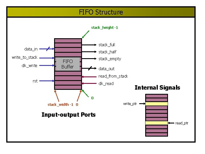
FIFO Structure stack_height -1 stack_full data_in write_to_stack clk_write stack_half stack_empty FIFO Buffer data_out read_from_stack rst clk_read Internal Signals 0 stack_width -1 0 write_ptr Input-output Ports read_ptr

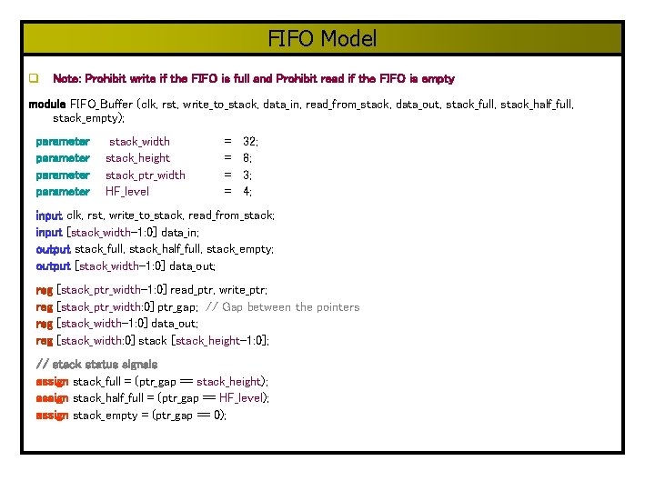
FIFO Model q Note: Prohibit write if the FIFO is full and Prohibit read if the FIFO is empty module FIFO_Buffer (clk, rst, write_to_stack, data_in, read_from_stack, data_out, stack_full, stack_half_full, stack_empty); parameter stack_width stack_height stack_ptr_width HF_level = = 32; 8; 3; 4; input clk, rst, write_to_stack, read_from_stack; input [stack_width-1: 0] data_in; output stack_full, stack_half_full, stack_empty; output [stack_width-1: 0] data_out; reg reg [stack_ptr_width-1: 0] read_ptr, write_ptr; [stack_ptr_width: 0] ptr_gap; // Gap between the pointers [stack_width-1: 0] data_out; [stack_width: 0] stack [stack_height-1: 0]; // stack status signals assign stack_full = (ptr_gap == stack_height); assign stack_half_full = (ptr_gap == HF_level); assign stack_empty = (ptr_gap == 0);

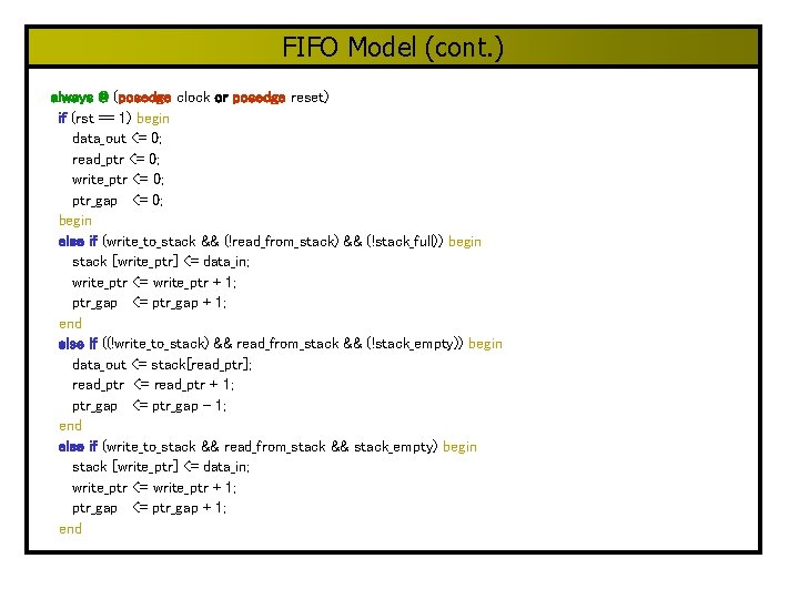
FIFO Model (cont. ) always @ (posedge clock or posedge reset) if (rst == 1) begin data_out <= 0; read_ptr <= 0; write_ptr <= 0; ptr_gap <= 0; begin else if (write_to_stack && (!read_from_stack) && (!stack_full)) begin stack [write_ptr] <= data_in; write_ptr <= write_ptr + 1; ptr_gap <= ptr_gap + 1; end else if ((!write_to_stack) && read_from_stack && (!stack_empty)) begin data_out <= stack[read_ptr]; read_ptr <= read_ptr + 1; ptr_gap <= ptr_gap - 1; end else if (write_to_stack && read_from_stack && stack_empty) begin stack [write_ptr] <= data_in; write_ptr <= write_ptr + 1; ptr_gap <= ptr_gap + 1; end

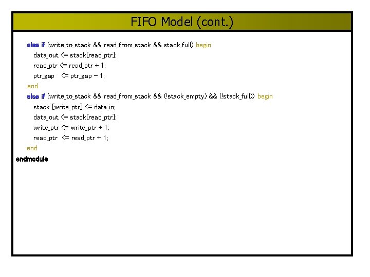
FIFO Model (cont. ) else if (write_to_stack && read_from_stack && stack_full) begin data_out <= stack[read_ptr]; read_ptr <= read_ptr + 1; ptr_gap <= ptr_gap - 1; end else if (write_to_stack && read_from_stack && (!stack_empty) && (!stack_full)) begin stack [write_ptr] <= data_in; data_out <= stack[read_ptr]; write_ptr <= write_ptr + 1; read_ptr <= read_ptr + 1; endmodule