Film Deposition in IC Fabrication Metal ContactsConnections Electrodes

Film Deposition in IC Fabrication Metal Contacts/Connections Electrodes Masks Wire insulation Device encapsulation Low stress Adherent Uniformity, no pin holes Conformal step coverage Thermal & electrical stability
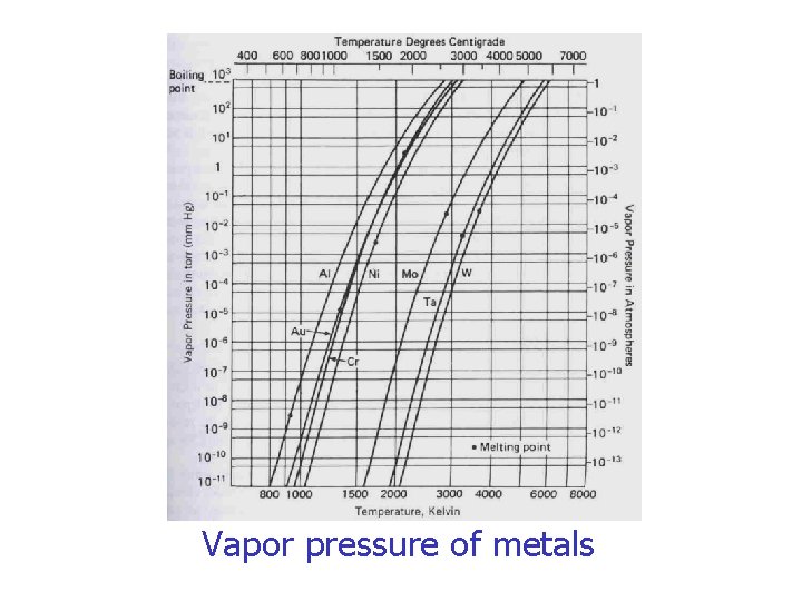
Vapor pressure of metals
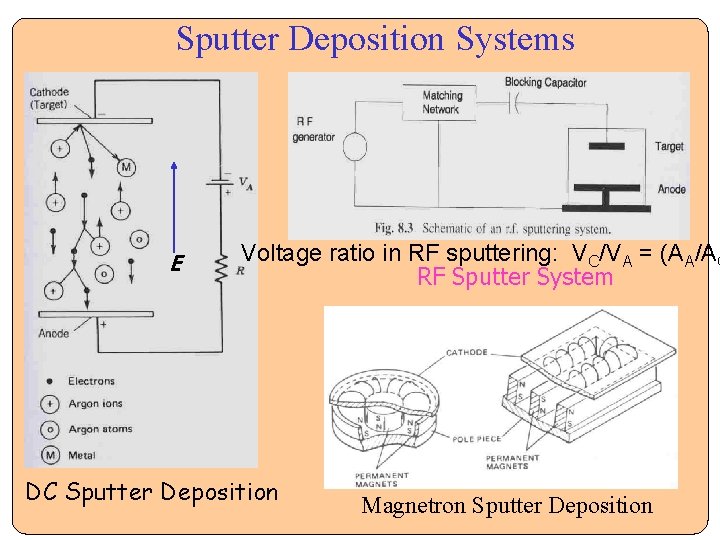
Sputter Deposition Systems E Voltage ratio in RF sputtering: VC/VA = (AA/AC RF Sputter System DC Sputter Deposition Magnetron Sputter Deposition
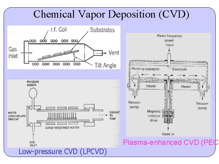
Chemical Vapor Deposition (CVD) Plasma-enhanced CVD (PECV Low-pressure CVD (LPCVD)
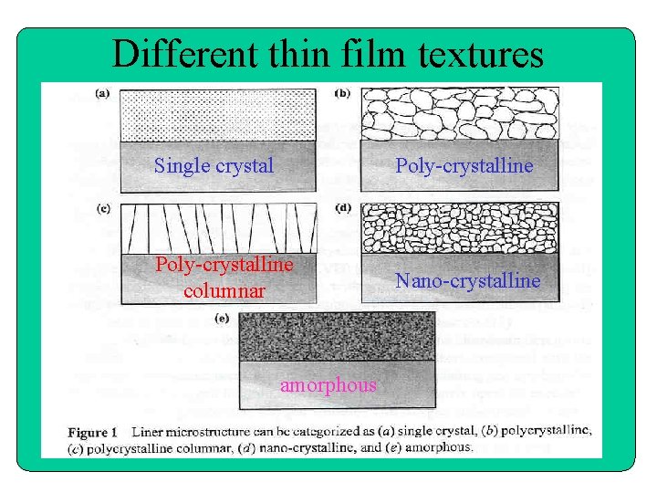
Different thin film textures Single crystal Poly-crystalline columnar Nano-crystalline amorphous
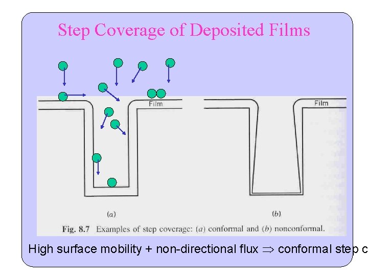
Step Coverage of Deposited Films High surface mobility + non-directional flux conformal step co
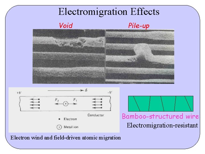
Electromigration Effects Void Pile-up Bamboo-structured wire Electromigration-resistant Electron wind and field-driven atomic migration
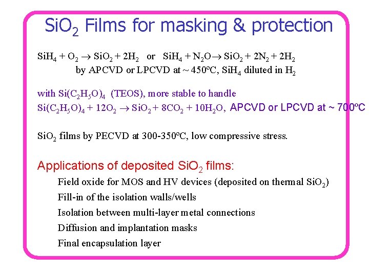
Si. O 2 Films for masking & protection Si. H 4 + O 2 Si. O 2 + 2 H 2 or Si. H 4 + N 2 O Si. O 2 + 2 N 2 + 2 H 2 by APCVD or LPCVD at ~ 450ºC, Si. H 4 diluted in H 2 with Si(C 2 H 5 O)4 (TEOS), more stable to handle Si(C 2 H 5 O)4 + 12 O 2 Si. O 2 + 8 CO 2 + 10 H 2 O, APCVD or LPCVD at ~ 700ºC Si. O 2 films by PECVD at 300 -350ºC, low compressive stress. Applications of deposited Si. O 2 films: Field oxide for MOS and HV devices (deposited on thermal Si. O 2) Fill-in of the isolation walls/wells Isolation between multi-layer metal connections Diffusion and implantation masks Final encapsulation layer
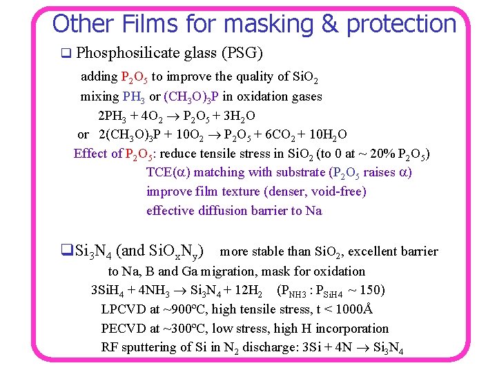
Other Films for masking & protection q Phosphosilicate glass (PSG) adding P 2 O 5 to improve the quality of Si. O 2 mixing PH 3 or (CH 3 O)3 P in oxidation gases 2 PH 3 + 4 O 2 P 2 O 5 + 3 H 2 O or 2(CH 3 O)3 P + 10 O 2 P 2 O 5 + 6 CO 2 + 10 H 2 O Effect of P 2 O 5: reduce tensile stress in Si. O 2 (to 0 at ~ 20% P 2 O 5) TCE( ) matching with substrate (P 2 O 5 raises ) improve film texture (denser, void-free) effective diffusion barrier to Na q. Si 3 N 4 (and Si. Ox. Ny) more stable than Si. O 2, excellent barrier to Na, B and Ga migration, mask for oxidation 3 Si. H 4 + 4 NH 3 Si 3 N 4 + 12 H 2 (PNH 3 : PSi. H 4 ~ 150) LPCVD at ~900ºC, high tensile stress, t < 1000Å PECVD at ~300ºC, low stress, high H incorporation RF sputtering of Si in N 2 discharge: 3 Si + 4 N Si 3 N 4
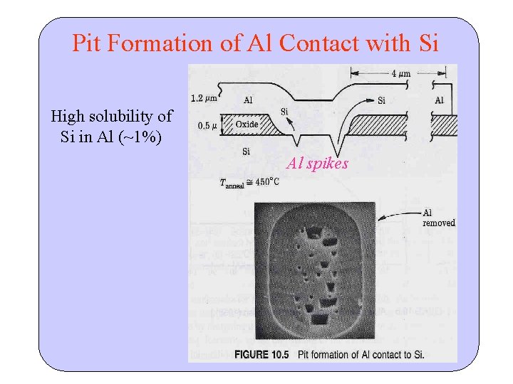
Pit Formation of Al Contact with Si High solubility of Si in Al (~1%) Al spikes
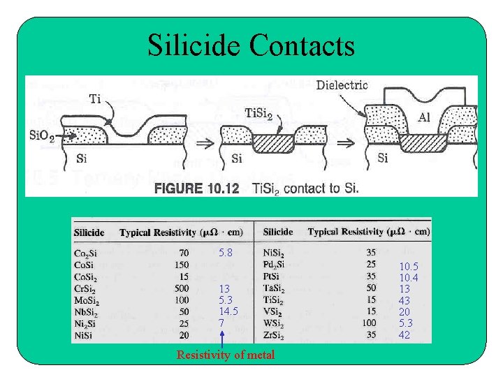
Silicide Contacts 5. 8 13 5. 3 14. 5 7 Resistivity of metal 10. 5 10. 4 13 43 20 5. 3 42
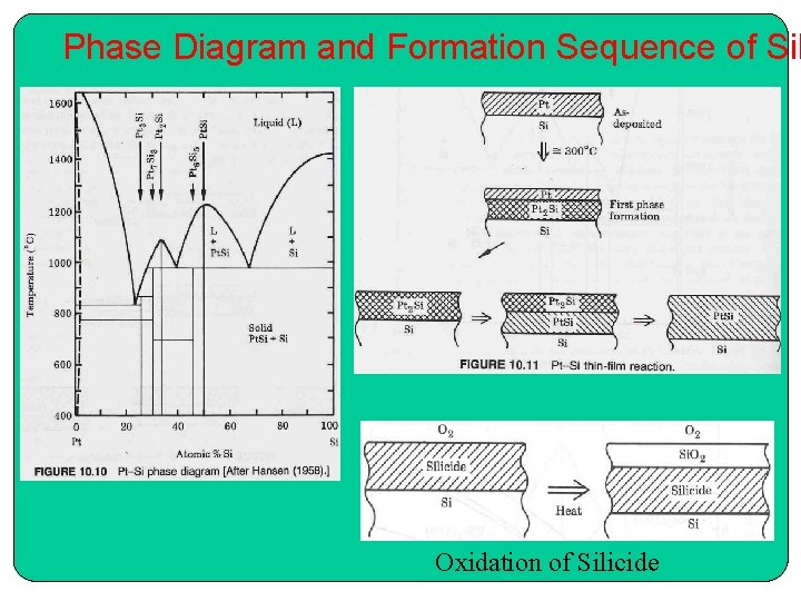
Phase Diagram and Formation Sequence of Sil Oxidation of Silicide
- Slides: 12