FIGURES FOR CHAPTER 9 MULTIPLEXERS DECODERS AND PROGRAMMABLE
FIGURES FOR CHAPTER 9 MULTIPLEXERS, DECODERS, AND PROGRAMMABLE LOGIC DEVICES This chapter in the book includes: Objectives Study Guide 9. 1 Introduction 9. 2 Multiplexers 9. 3 Three-State Buffers 9. 4 Decoders and Encoders 9. 5 Read-Only Memories 9. 6 Programmable Logic Devices 9. 7 Complex Programmable Logic Devices 9. 8 Field Programmable Gate Arrays Problems Click the mouse to move to the next page. Use the ESC key to exit this chapter. © 2004 Brooks/Cole
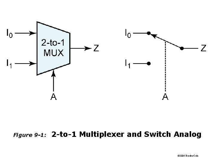
Figure 9 -1: 2 -to-1 Multiplexer and Switch Analog © 2004 Brooks/Cole
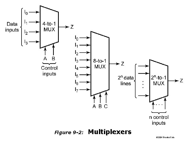
Figure 9 -2: Multiplexers © 2004 Brooks/Cole
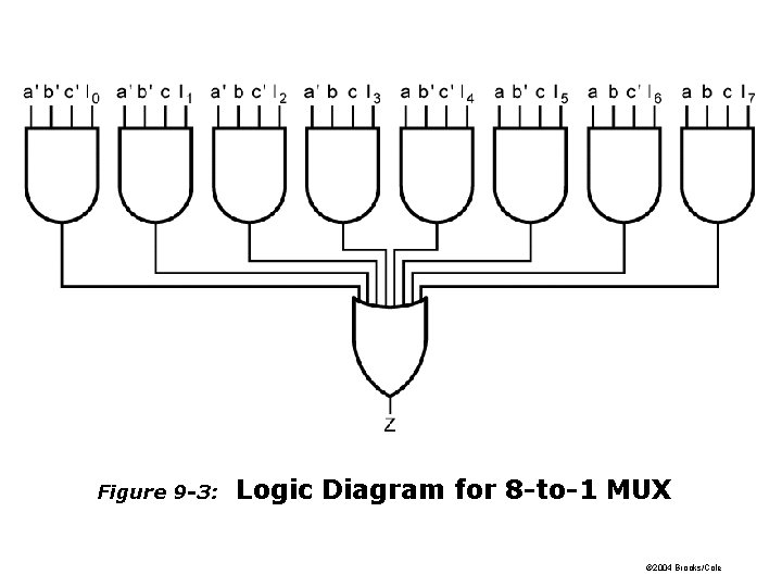
Figure 9 -3: Logic Diagram for 8 -to-1 MUX © 2004 Brooks/Cole
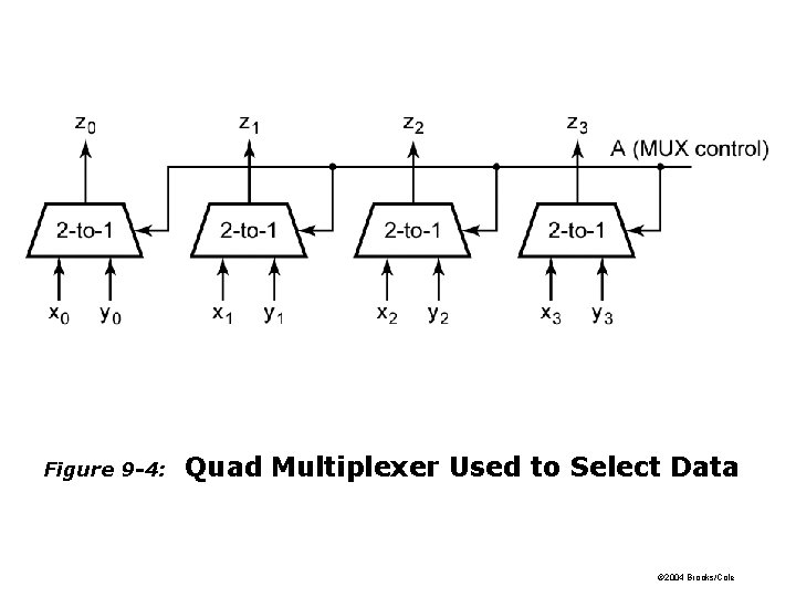
Figure 9 -4: Quad Multiplexer Used to Select Data © 2004 Brooks/Cole
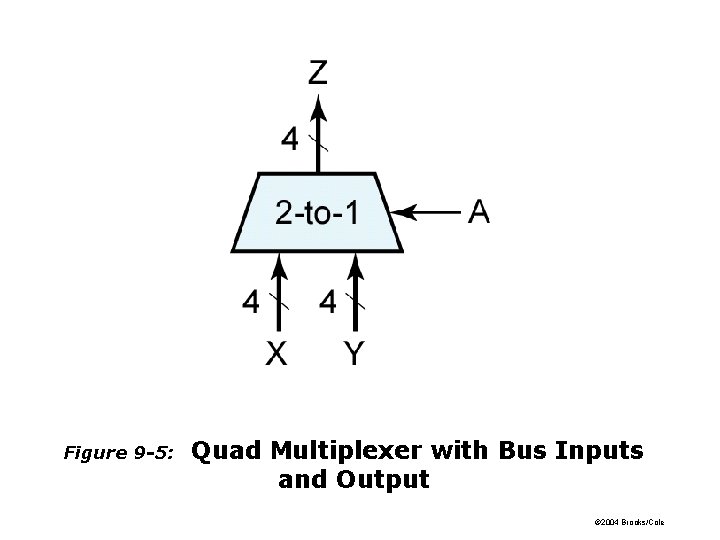
Figure 9 -5: Quad Multiplexer with Bus Inputs and Output © 2004 Brooks/Cole
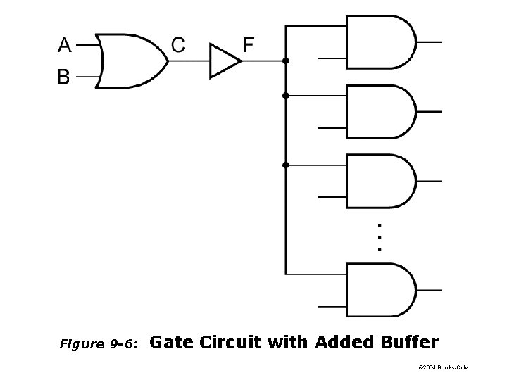
Figure 9 -6: Gate Circuit with Added Buffer © 2004 Brooks/Cole
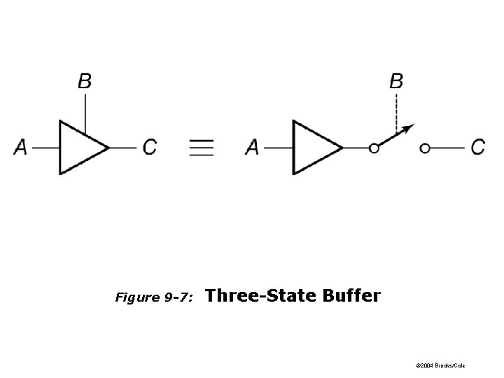
Figure 9 -7: Three-State Buffer © 2004 Brooks/Cole
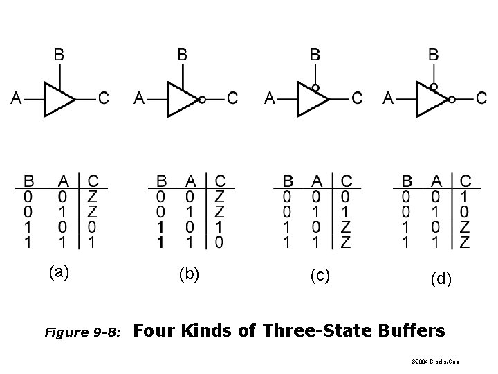
(a) Figure 9 -8: (b) (c) (d) Four Kinds of Three-State Buffers © 2004 Brooks/Cole
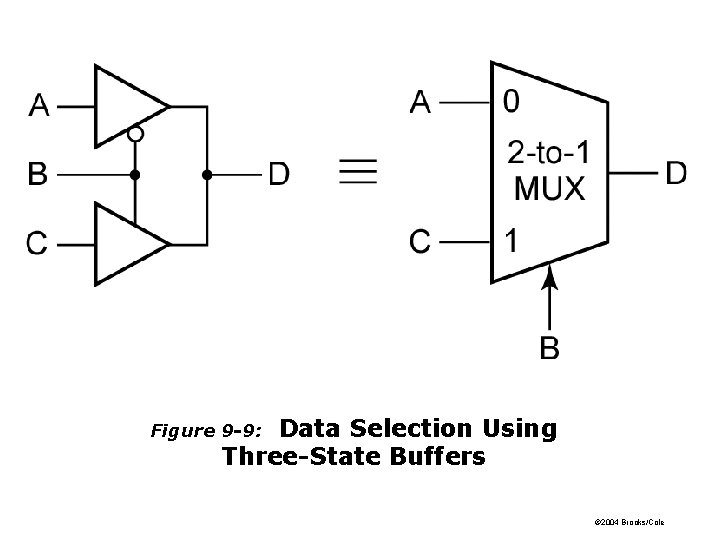
Data Selection Using Three-State Buffers Figure 9 -9: © 2004 Brooks/Cole
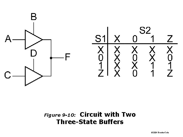
Circuit with Two Three-State Buffers Figure 9 -10: © 2004 Brooks/Cole
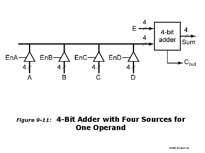
Figure 9 -11: 4 -Bit Adder with Four Sources for One Operand © 2004 Brooks/Cole
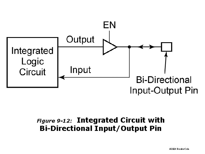
Integrated Circuit with Bi-Directional Input/Output Pin Figure 9 -12: © 2004 Brooks/Cole
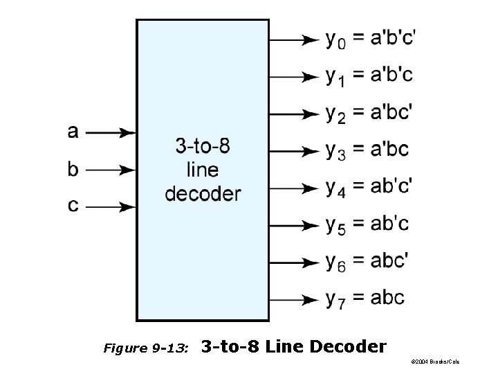
Figure 9 -13: 3 -to-8 Line Decoder © 2004 Brooks/Cole
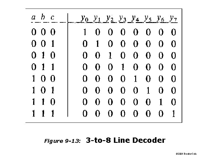
Figure 9 -13: 3 -to-8 Line Decoder © 2004 Brooks/Cole
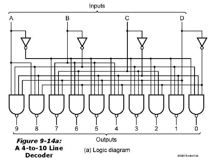
Figure 9 -14 a: A 4 -to-10 Line Decoder © 2004 Brooks/Cole
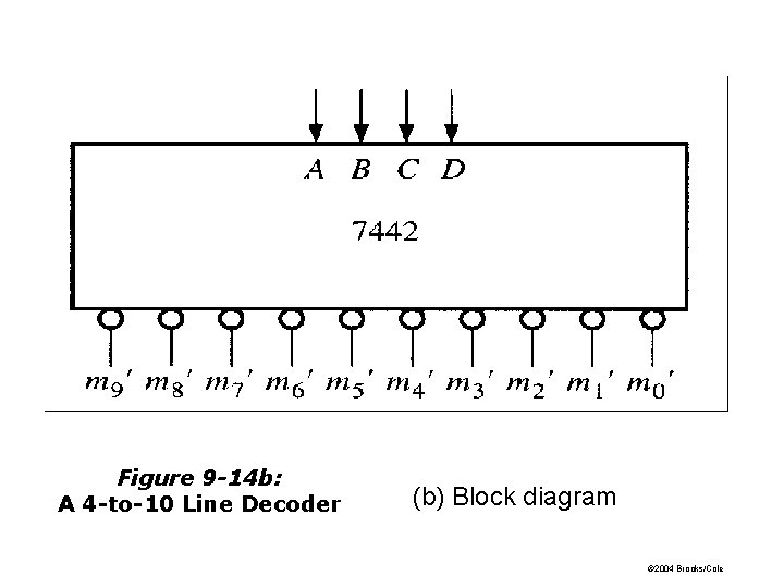
Figure 9 -14 b: A 4 -to-10 Line Decoder (b) Block diagram © 2004 Brooks/Cole
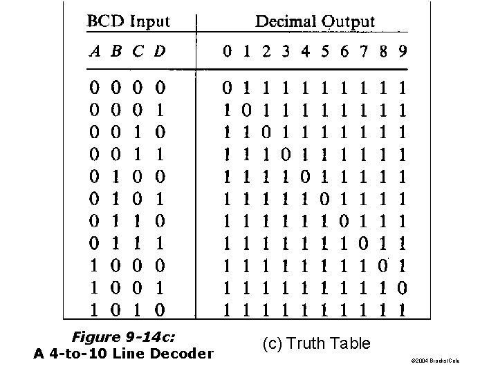
Figure 9 -14 c: A 4 -to-10 Line Decoder (c) Truth Table © 2004 Brooks/Cole
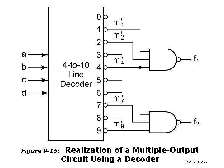
Figure 9 -15: Realization of a Multiple-Output Circuit Using a Decoder © 2004 Brooks/Cole
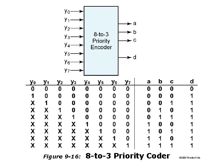
Figure 9 -16: 8 -to-3 Priority Coder © 2004 Brooks/Cole
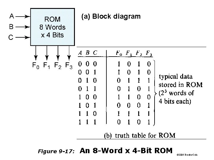
(a) Block diagram Figure 9 -17: An 8 -Word x 4 -Bit ROM © 2004 Brooks/Cole
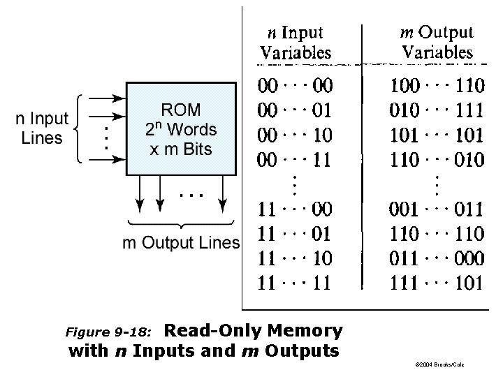
Read-Only Memory with n Inputs and m Outputs Figure 9 -18: © 2004 Brooks/Cole
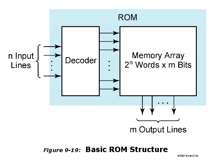
Figure 9 -19: Basic ROM Structure © 2004 Brooks/Cole
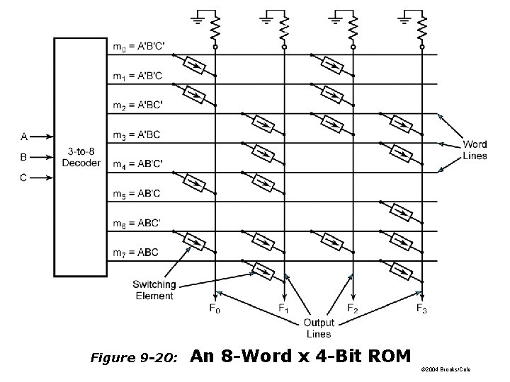
Figure 9 -20: An 8 -Word x 4 -Bit ROM © 2004 Brooks/Cole
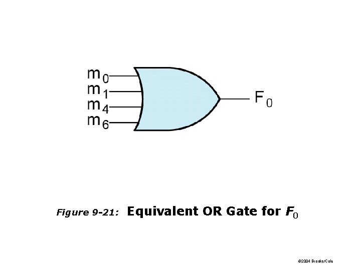
Figure 9 -21: Equivalent OR Gate for F 0 © 2004 Brooks/Cole
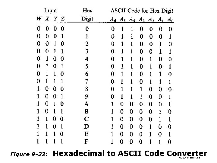
Figure 9 -22: Hexadecimal to ASCII Code Converter © 2004 Brooks/Cole
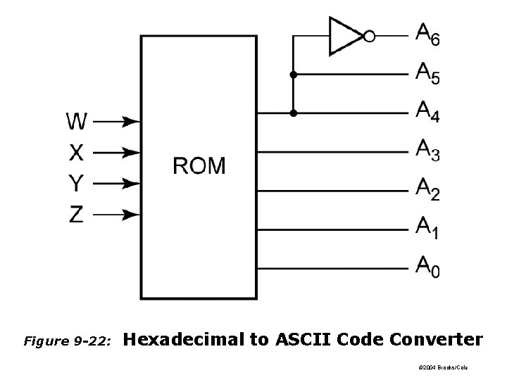
Figure 9 -22: Hexadecimal to ASCII Code Converter © 2004 Brooks/Cole
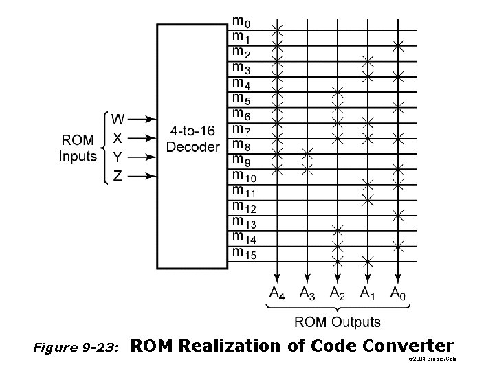
Figure 9 -23: ROM Realization of Code Converter © 2004 Brooks/Cole
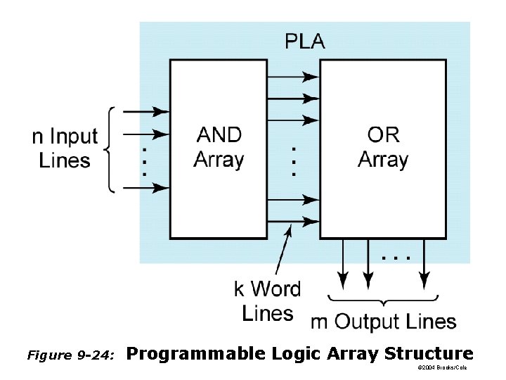
Figure 9 -24: Programmable Logic Array Structure © 2004 Brooks/Cole
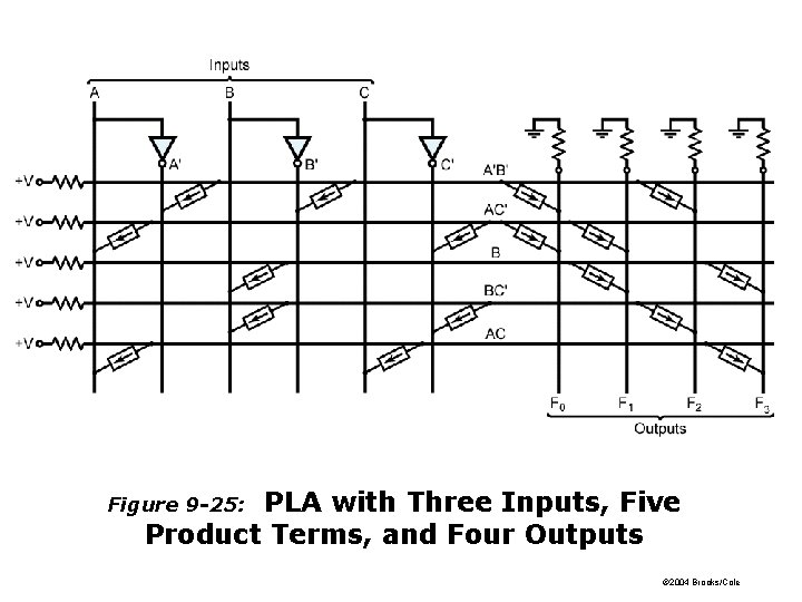
PLA with Three Inputs, Five Product Terms, and Four Outputs Figure 9 -25: © 2004 Brooks/Cole
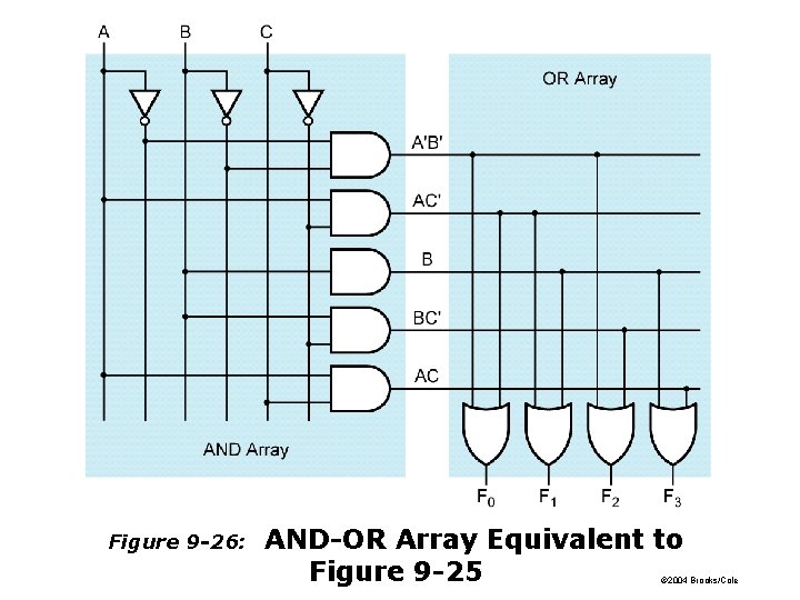
Figure 9 -26: AND-OR Array Equivalent to Figure 9 -25 © 2004 Brooks/Cole
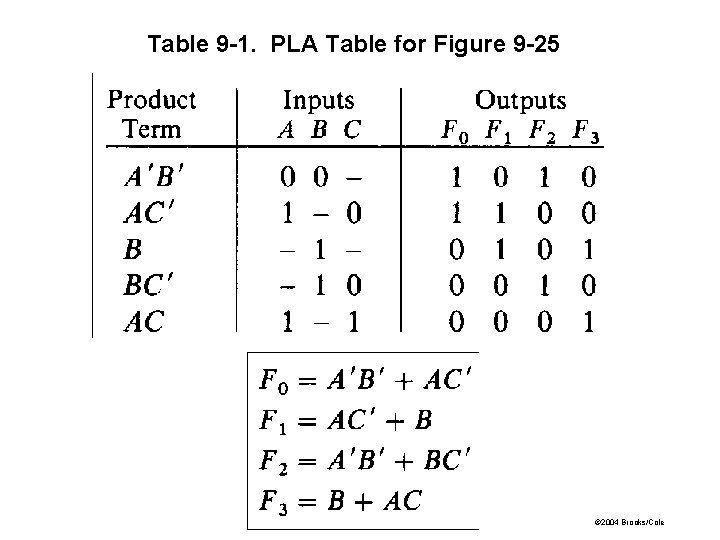
Table 9 -1. PLA Table for Figure 9 -25 © 2004 Brooks/Cole
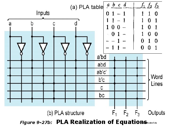
(a) PLA table Figure 9 -27 b: PLA Realization of Equations © 2004 Brooks/Cole
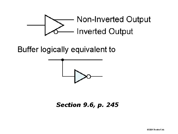
Buffer logically equivalent to Section 9. 6, p. 245 © 2004 Brooks/Cole
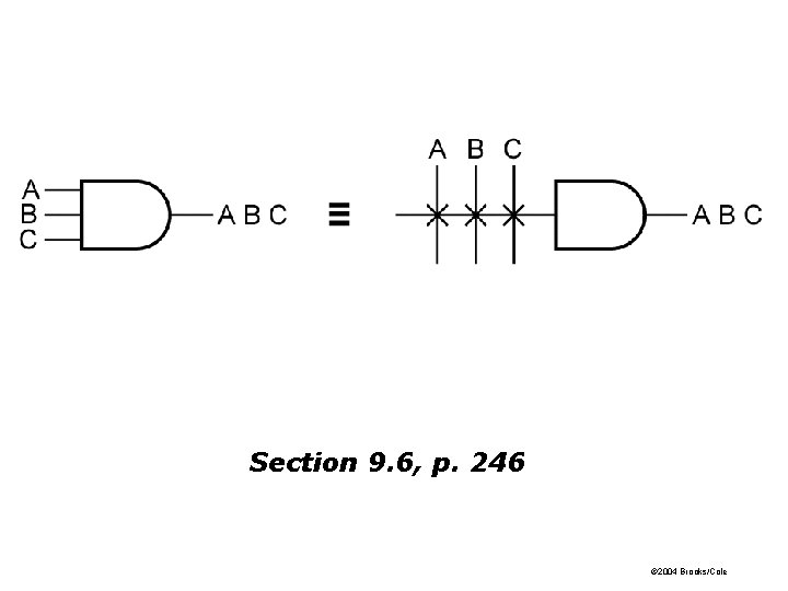
Section 9. 6, p. 246 © 2004 Brooks/Cole
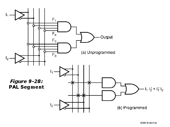
Figure 9 -28: PAL Segment © 2004 Brooks/Cole
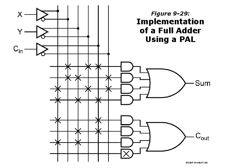
Figure 9 -29: Implementation of a Full Adder Using a PAL © 2004 Brooks/Cole
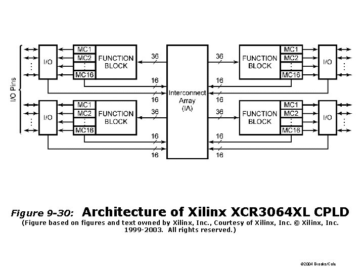
Figure 9 -30: Architecture of Xilinx XCR 3064 XL CPLD (Figure based on figures and text owned by Xilinx, Inc. , Courtesy of Xilinx, Inc. © Xilinx, Inc. 1999 -2003. All rights reserved. ) © 2004 Brooks/Cole
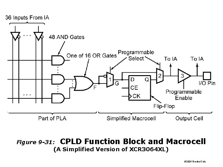
Figure 9 -31: CPLD Function Block and Macrocell (A Simplified Version of XCR 3064 XL) © 2004 Brooks/Cole
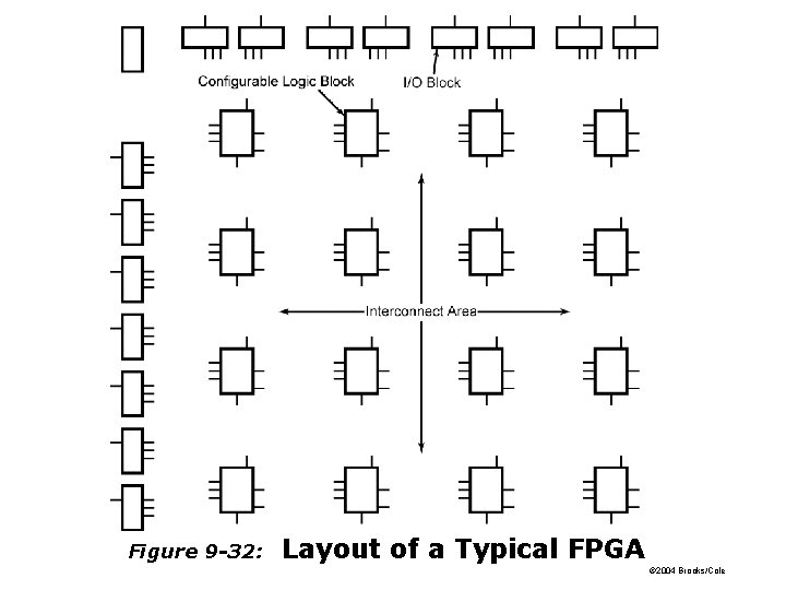
Figure 9 -32: Layout of a Typical FPGA © 2004 Brooks/Cole
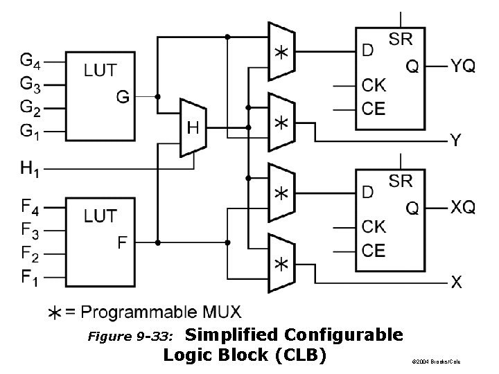
Simplified Configurable Logic Block (CLB) Figure 9 -33: © 2004 Brooks/Cole
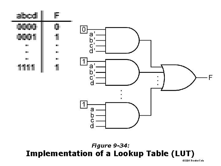
Figure 9 -34: Implementation of a Lookup Table (LUT) © 2004 Brooks/Cole
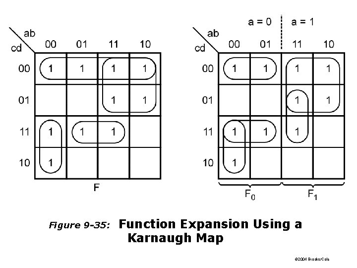
Figure 9 -35: Function Expansion Using a Karnaugh Map © 2004 Brooks/Cole
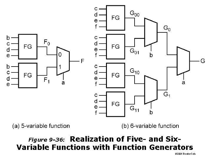
Realization of Five- and Six. Variable Functions with Function Generators Figure 9 -36: © 2004 Brooks/Cole
- Slides: 44