
Figure 9 1 Architecture of a Simple Computer

- Slides: 17
Figure 9. 1 Architecture of a Simple Computer System.
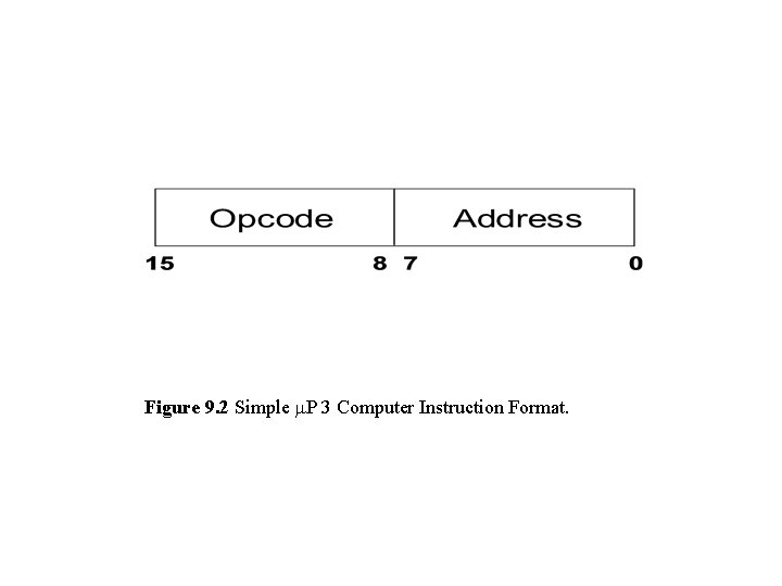
Figure 9. 2 Simple m. P 3 Computer Instruction Format.
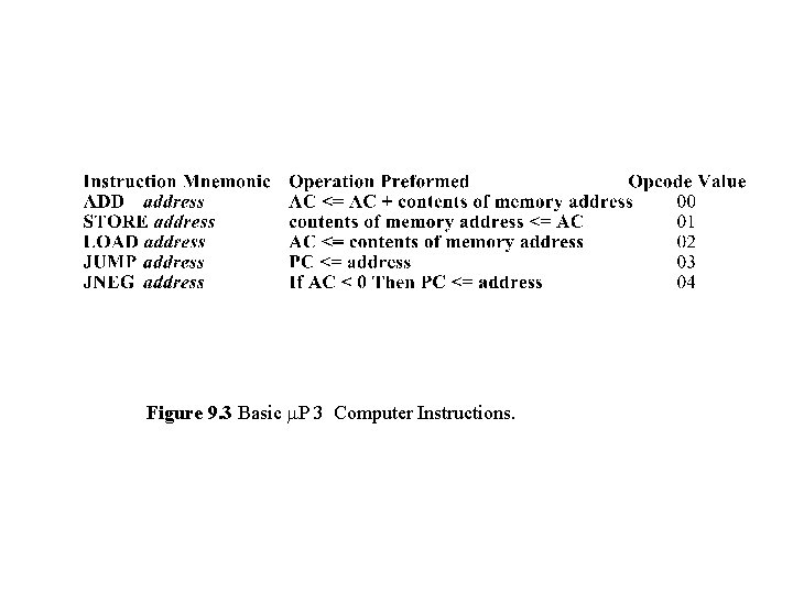
Figure 9. 3 Basic m. P 3 Computer Instructions.
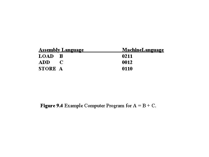
Assembly Language LOAD B ADD C STORE A Machine. Language 0211 0012 0110 Figure 9. 4 Example Computer Program for A = B + C.
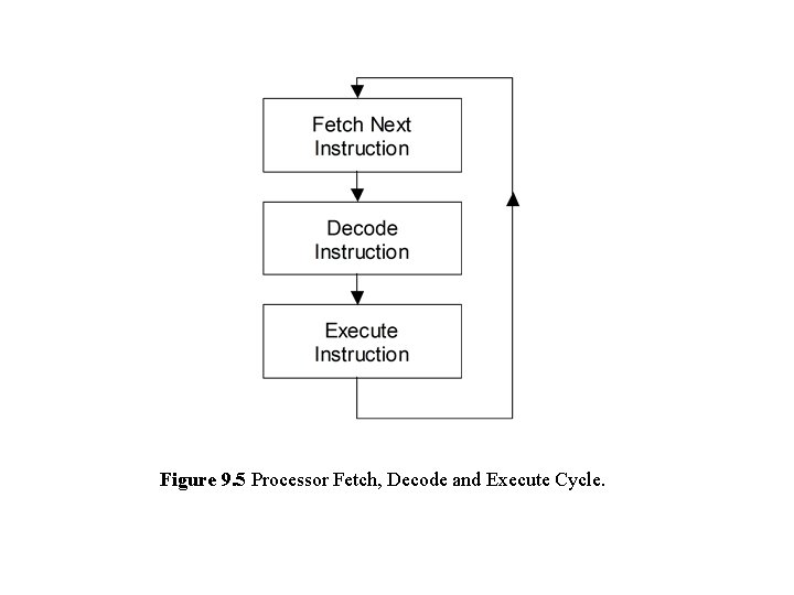
Figure 9. 5 Processor Fetch, Decode and Execute Cycle.
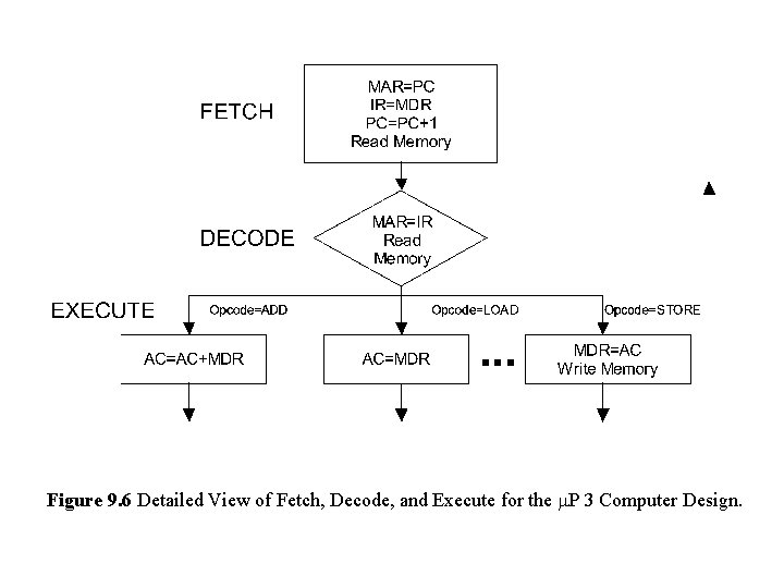
Figure 9. 6 Detailed View of Fetch, Decode, and Execute for the m. P 3 Computer Design.
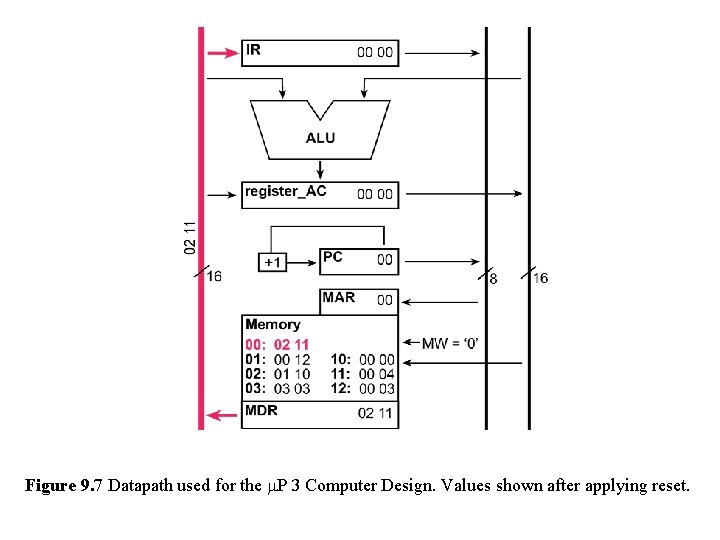
Figure 9. 7 Datapath used for the m. P 3 Computer Design. Values shown after applying reset.
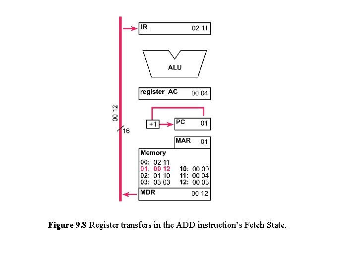
Figure 9. 8 Register transfers in the ADD instruction’s Fetch State.
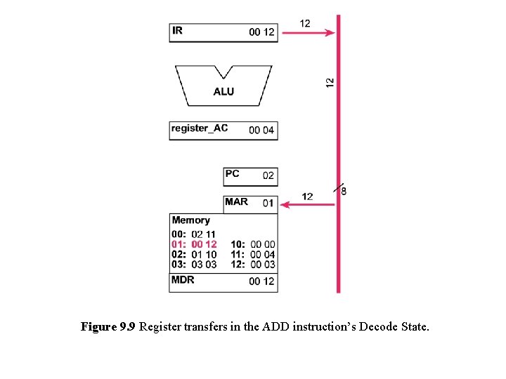
Figure 9. 9 Register transfers in the ADD instruction’s Decode State.
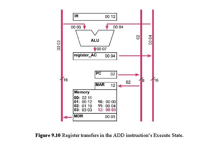
Figure 9. 10 Register transfers in the ADD instruction’s Execute State.
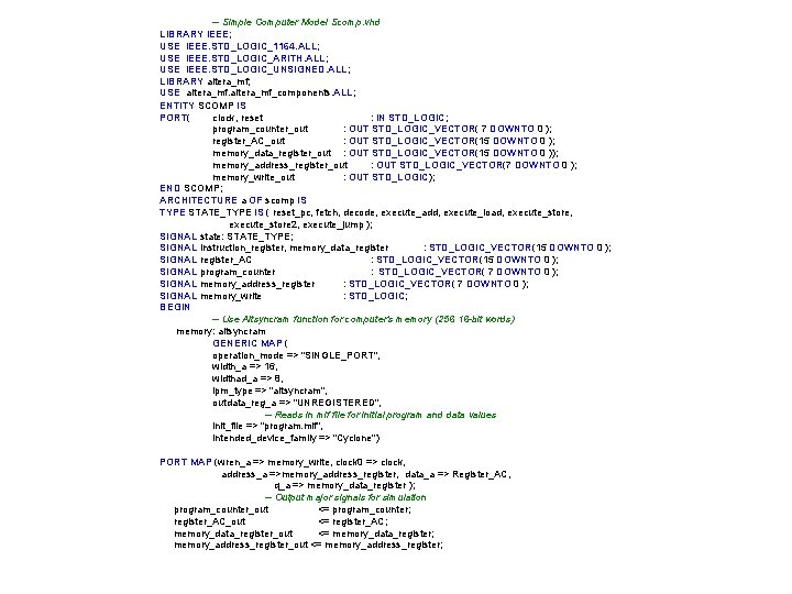
-- Simple Computer Model Scomp. vhd LIBRARY IEEE; USE IEEE. STD_LOGIC_1164. ALL; USE IEEE. STD_LOGIC_ARITH. ALL; USE IEEE. STD_LOGIC_UNSIGNED. ALL; LIBRARY altera_mf; USE altera_mf_components. ALL; ENTITY SCOMP IS PORT( clock, reset : IN STD_LOGIC; program_counter_out : OUT STD_LOGIC_VECTOR( 7 DOWNTO 0 ); register_AC_out : OUT STD_LOGIC_VECTOR(15 DOWNTO 0 ); memory_data_register_out : OUT STD_LOGIC_VECTOR(15 DOWNTO 0 )); memory_address_register_out : OUT STD_LOGIC_VECTOR(7 DOWNTO 0 ); memory_write_out : OUT STD_LOGIC); END SCOMP; ARCHITECTURE a OF scomp IS TYPE STATE_TYPE IS ( reset_pc, fetch, decode, execute_add, execute_load, execute_store 2, execute_jump ); SIGNAL state: STATE_TYPE; SIGNAL instruction_register, memory_data_register : STD_LOGIC_VECTOR(15 DOWNTO 0 ); SIGNAL register_AC : STD_LOGIC_VECTOR(15 DOWNTO 0 ); SIGNAL program_counter : STD_LOGIC_VECTOR( 7 DOWNTO 0 ); SIGNAL memory_address_register : STD_LOGIC_VECTOR( 7 DOWNTO 0 ); SIGNAL memory_write : STD_LOGIC; BEGIN -- Use Altsyncram function for computer's memory (256 16 -bit words) memory: altsyncram GENERIC MAP ( operation_mode => "SINGLE_PORT", width_a => 16, widthad_a => 8, lpm_type => "altsyncram", outdata_reg_a => "UNREGISTERED", -- Reads in mif file for initial program and data values init_file => "program. mif", intended_device_family => "Cyclone") PORT MAP (wren_a => memory_write, clock 0 => clock, address_a =>memory_address_register, data_a => Register_AC, q_a => memory_data_register ); -- Output major signals for simulation program_counter_out <= program_counter; register_AC_out <= register_AC; memory_data_register_out <= memory_data_register; memory_address_register_out <= memory_address_register;
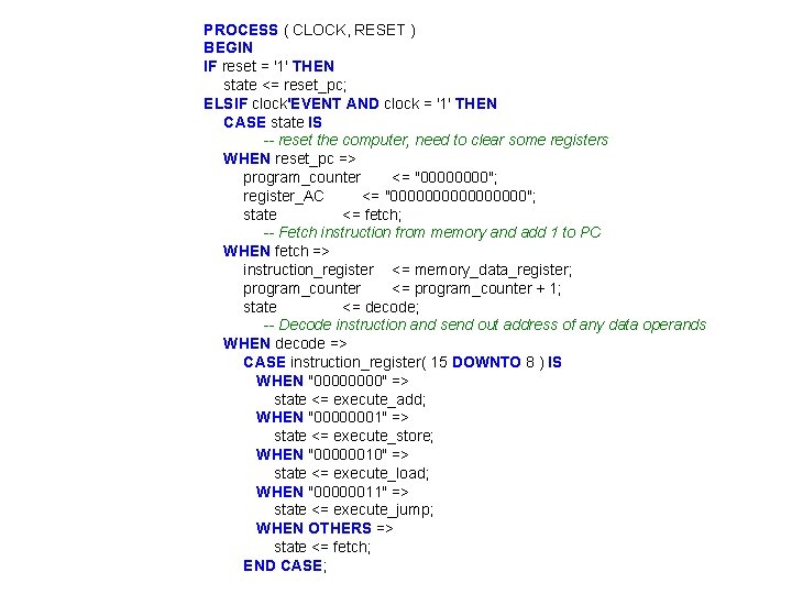
PROCESS ( CLOCK, RESET ) BEGIN IF reset = '1' THEN state <= reset_pc; ELSIF clock'EVENT AND clock = '1' THEN CASE state IS -- reset the computer, need to clear some registers WHEN reset_pc => program_counter <= "0000"; register_AC <= "00000000"; state <= fetch; -- Fetch instruction from memory and add 1 to PC WHEN fetch => instruction_register <= memory_data_register; program_counter <= program_counter + 1; state <= decode; -- Decode instruction and send out address of any data operands WHEN decode => CASE instruction_register( 15 DOWNTO 8 ) IS WHEN "0000" => state <= execute_add; WHEN "00000001" => state <= execute_store; WHEN "00000010" => state <= execute_load; WHEN "00000011" => state <= execute_jump; WHEN OTHERS => state <= fetch; END CASE;
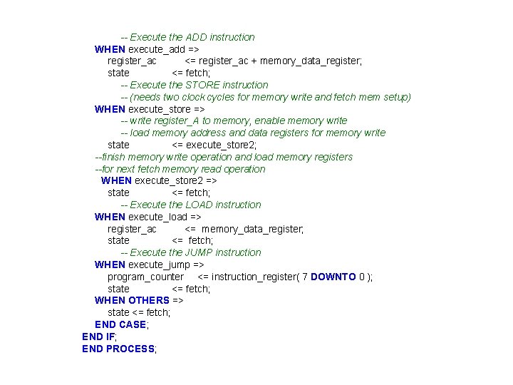
-- Execute the ADD instruction WHEN execute_add => register_ac <= register_ac + memory_data_register; state <= fetch; -- Execute the STORE instruction -- (needs two clock cycles for memory write and fetch mem setup) WHEN execute_store => -- write register_A to memory, enable memory write -- load memory address and data registers for memory write state <= execute_store 2; --finish memory write operation and load memory registers --for next fetch memory read operation WHEN execute_store 2 => state <= fetch; -- Execute the LOAD instruction WHEN execute_load => register_ac <= memory_data_register; state <= fetch; -- Execute the JUMP instruction WHEN execute_jump => program_counter <= instruction_register( 7 DOWNTO 0 ); state <= fetch; WHEN OTHERS => state <= fetch; END CASE; END IF; END PROCESS;
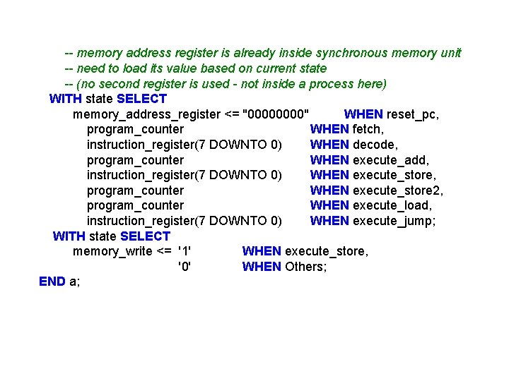
-- memory address register is already inside synchronous memory unit -- need to load its value based on current state -- (no second register is used - not inside a process here) WITH state SELECT memory_address_register <= "0000" WHEN reset_pc, program_counter WHEN fetch, instruction_register(7 DOWNTO 0) WHEN decode, program_counter WHEN execute_add, instruction_register(7 DOWNTO 0) WHEN execute_store, program_counter WHEN execute_store 2, program_counter WHEN execute_load, instruction_register(7 DOWNTO 0) WHEN execute_jump; WITH state SELECT memory_write <= '1' WHEN execute_store, '0' WHEN Others; END a;
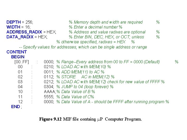
DEPTH = 256; % Memory depth and width are required % WIDTH = 16; % Enter a decimal number % ADDRESS_RADIX = HEX; % Address and value radixes are optional % DATA_RADIX = HEX; % Enter BIN, DEC, HEX, or OCT; unless % % otherwise specified, radixes = HEX % -- Specify values for addresses, which can be single address or range CONTENT BEGIN [00. . FF] : 0000; % Range--Every address from 00 to FF = 0000 (Default) 00 : 0210; % LOAD AC with MEM(10) % 01 : 0011; % ADD MEM(11) to AC % 02 : 0112; % STORE AC in MEM(12) % 03 : 0212; % LOAD AC with MEM(12) check for new value of FFFF % 04 : 0304; % JUMP to 04 (loop forever) % 10 : AAAA; % Data Value of B % 11 : 5555; % Data Value of C% 12 : 0000; % Data Value of A - should be FFFF after running program % END ; Figure 9. 12 MIF file containg m. P Computer Program. %
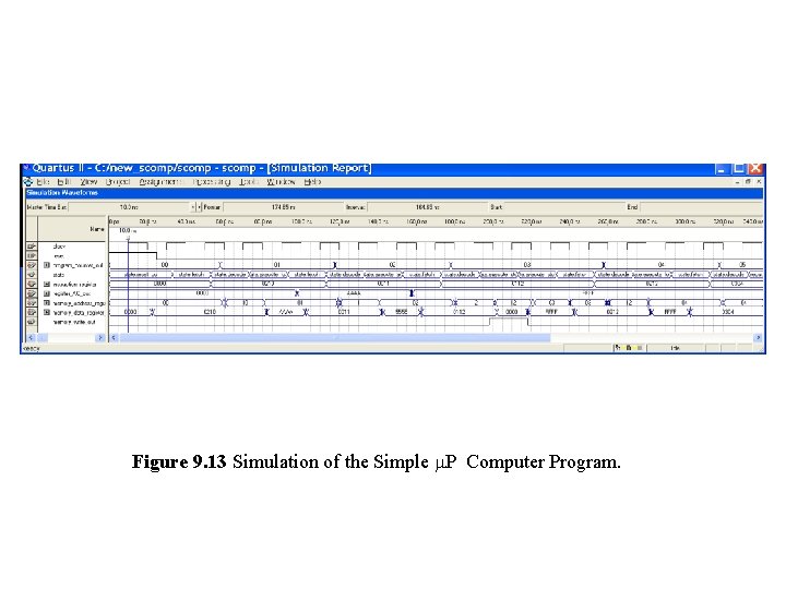
Figure 9. 13 Simulation of the Simple m. P Computer Program.
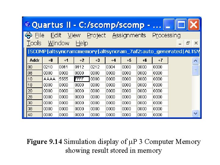
Figure 9. 14 Simulation display of m. P 3 Computer Memory showing result stored in memory