FIGURE 6 1 Fourbit register Digital Design With
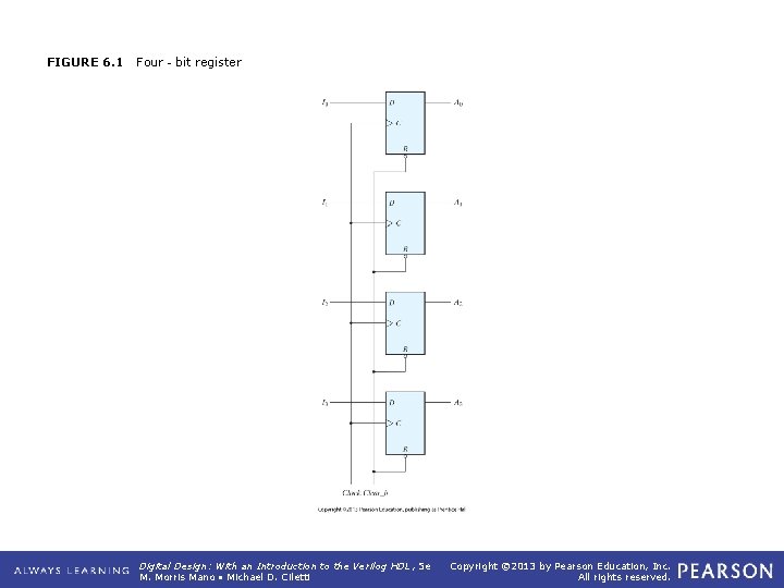
FIGURE 6. 1 Four‐bit register Digital Design: With an Introduction to the Verilog HDL, 5 e M. Morris Mano • Michael D. Ciletti Copyright © 2013 by Pearson Education, Inc. All rights reserved.
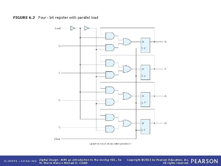
FIGURE 6. 2 Four‐bit register with parallel load Digital Design: With an Introduction to the Verilog HDL, 5 e M. Morris Mano • Michael D. Ciletti Copyright © 2013 by Pearson Education, Inc. All rights reserved.
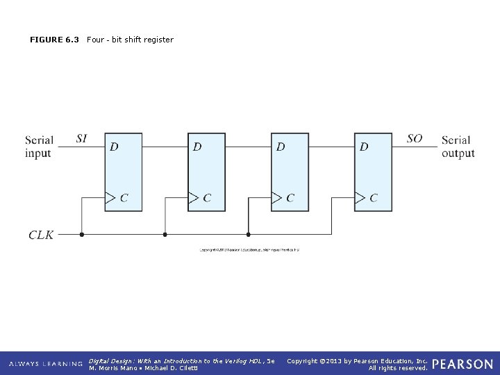
FIGURE 6. 3 Four‐bit shift register Digital Design: With an Introduction to the Verilog HDL, 5 e M. Morris Mano • Michael D. Ciletti Copyright © 2013 by Pearson Education, Inc. All rights reserved.
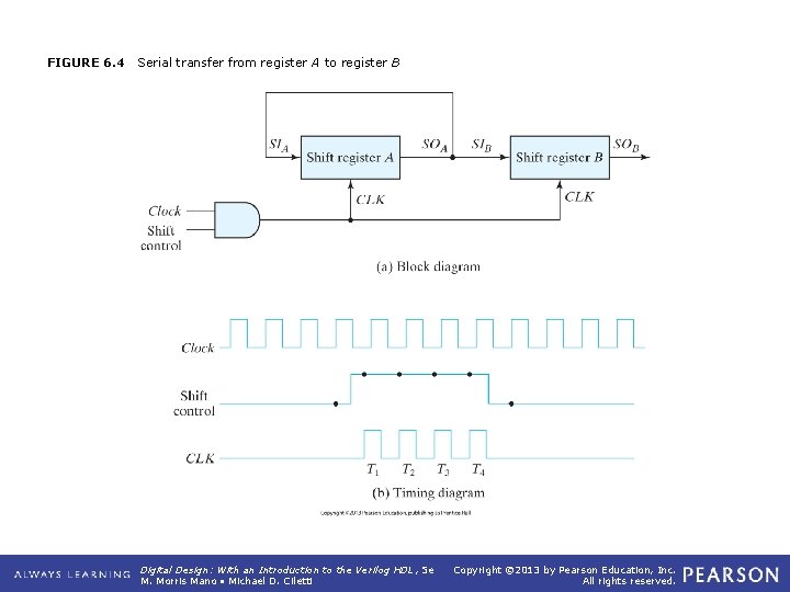
FIGURE 6. 4 Serial transfer from register A to register B Digital Design: With an Introduction to the Verilog HDL, 5 e M. Morris Mano • Michael D. Ciletti Copyright © 2013 by Pearson Education, Inc. All rights reserved.
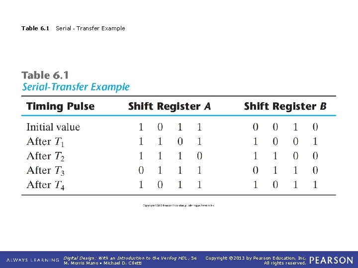
Table 6. 1 Serial‐Transfer Example Digital Design: With an Introduction to the Verilog HDL, 5 e M. Morris Mano • Michael D. Ciletti Copyright © 2013 by Pearson Education, Inc. All rights reserved.
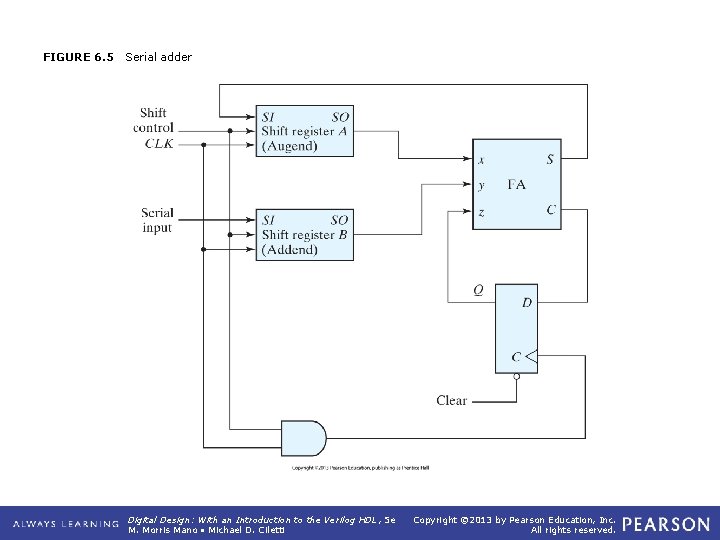
FIGURE 6. 5 Serial adder Digital Design: With an Introduction to the Verilog HDL, 5 e M. Morris Mano • Michael D. Ciletti Copyright © 2013 by Pearson Education, Inc. All rights reserved.
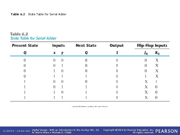
Table 6. 2 State Table for Serial Adder Digital Design: With an Introduction to the Verilog HDL, 5 e M. Morris Mano • Michael D. Ciletti Copyright © 2013 by Pearson Education, Inc. All rights reserved.
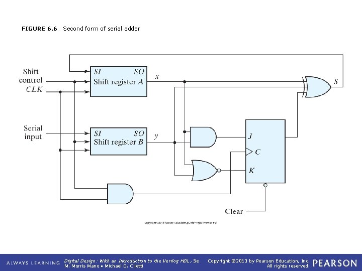
FIGURE 6. 6 Second form of serial adder Digital Design: With an Introduction to the Verilog HDL, 5 e M. Morris Mano • Michael D. Ciletti Copyright © 2013 by Pearson Education, Inc. All rights reserved.
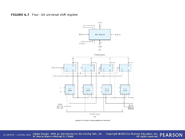
FIGURE 6. 7 Four‐bit universal shift register Digital Design: With an Introduction to the Verilog HDL, 5 e M. Morris Mano • Michael D. Ciletti Copyright © 2013 by Pearson Education, Inc. All rights reserved.
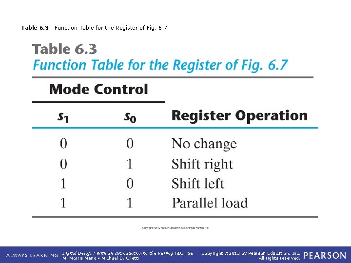
Table 6. 3 Function Table for the Register of Fig. 6. 7 Digital Design: With an Introduction to the Verilog HDL, 5 e M. Morris Mano • Michael D. Ciletti Copyright © 2013 by Pearson Education, Inc. All rights reserved.
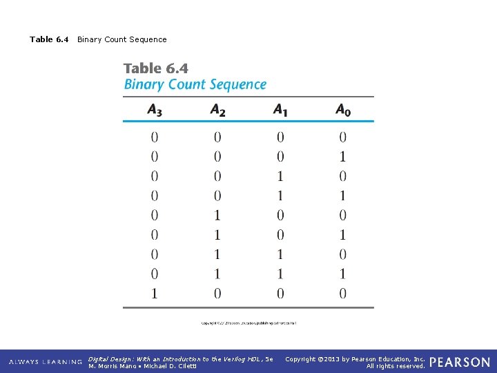
Table 6. 4 Binary Count Sequence Digital Design: With an Introduction to the Verilog HDL, 5 e M. Morris Mano • Michael D. Ciletti Copyright © 2013 by Pearson Education, Inc. All rights reserved.
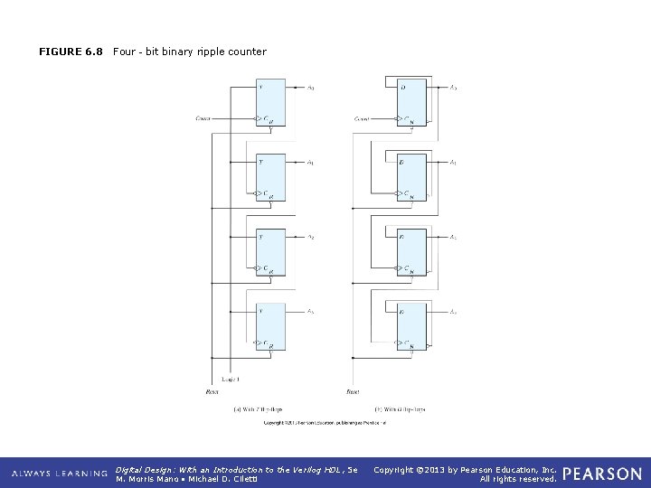
FIGURE 6. 8 Four‐bit binary ripple counter Digital Design: With an Introduction to the Verilog HDL, 5 e M. Morris Mano • Michael D. Ciletti Copyright © 2013 by Pearson Education, Inc. All rights reserved.
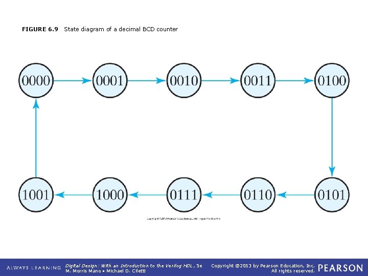
FIGURE 6. 9 State diagram of a decimal BCD counter Digital Design: With an Introduction to the Verilog HDL, 5 e M. Morris Mano • Michael D. Ciletti Copyright © 2013 by Pearson Education, Inc. All rights reserved.
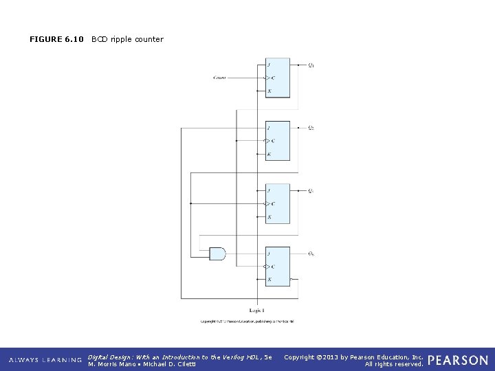
FIGURE 6. 10 BCD ripple counter Digital Design: With an Introduction to the Verilog HDL, 5 e M. Morris Mano • Michael D. Ciletti Copyright © 2013 by Pearson Education, Inc. All rights reserved.
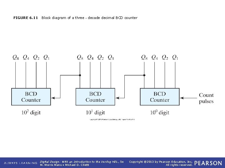
FIGURE 6. 11 Block diagram of a three‐decade decimal BCD counter Digital Design: With an Introduction to the Verilog HDL, 5 e M. Morris Mano • Michael D. Ciletti Copyright © 2013 by Pearson Education, Inc. All rights reserved.
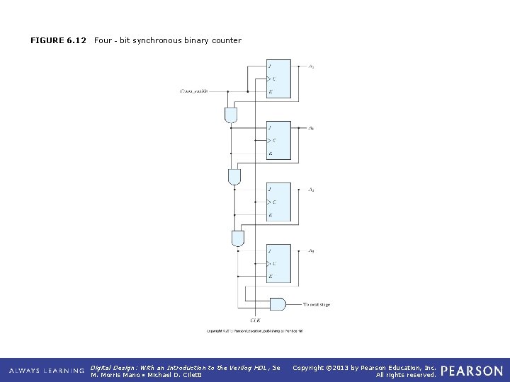
FIGURE 6. 12 Four‐bit synchronous binary counter Digital Design: With an Introduction to the Verilog HDL, 5 e M. Morris Mano • Michael D. Ciletti Copyright © 2013 by Pearson Education, Inc. All rights reserved.
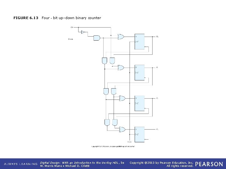
FIGURE 6. 13 Four‐bit up–down binary counter Digital Design: With an Introduction to the Verilog HDL, 5 e M. Morris Mano • Michael D. Ciletti Copyright © 2013 by Pearson Education, Inc. All rights reserved.
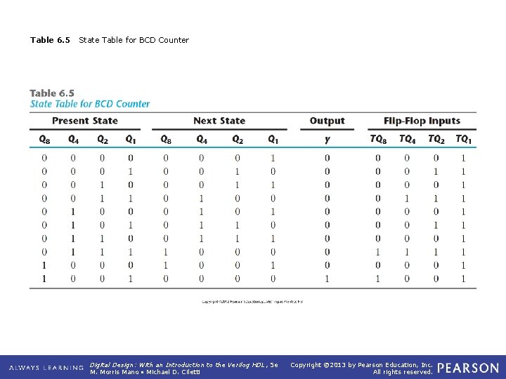
Table 6. 5 State Table for BCD Counter Digital Design: With an Introduction to the Verilog HDL, 5 e M. Morris Mano • Michael D. Ciletti Copyright © 2013 by Pearson Education, Inc. All rights reserved.
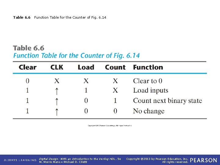
Table 6. 6 Function Table for the Counter of Fig. 6. 14 Digital Design: With an Introduction to the Verilog HDL, 5 e M. Morris Mano • Michael D. Ciletti Copyright © 2013 by Pearson Education, Inc. All rights reserved.
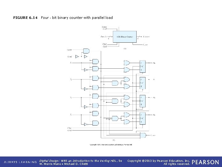
FIGURE 6. 14 Four‐bit binary counter with parallel load Digital Design: With an Introduction to the Verilog HDL, 5 e M. Morris Mano • Michael D. Ciletti Copyright © 2013 by Pearson Education, Inc. All rights reserved.
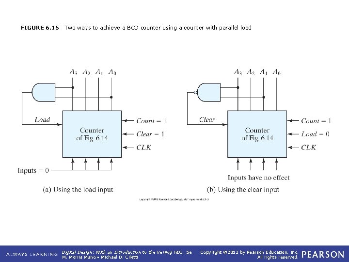
FIGURE 6. 15 Two ways to achieve a BCD counter using a counter with parallel load Digital Design: With an Introduction to the Verilog HDL, 5 e M. Morris Mano • Michael D. Ciletti Copyright © 2013 by Pearson Education, Inc. All rights reserved.
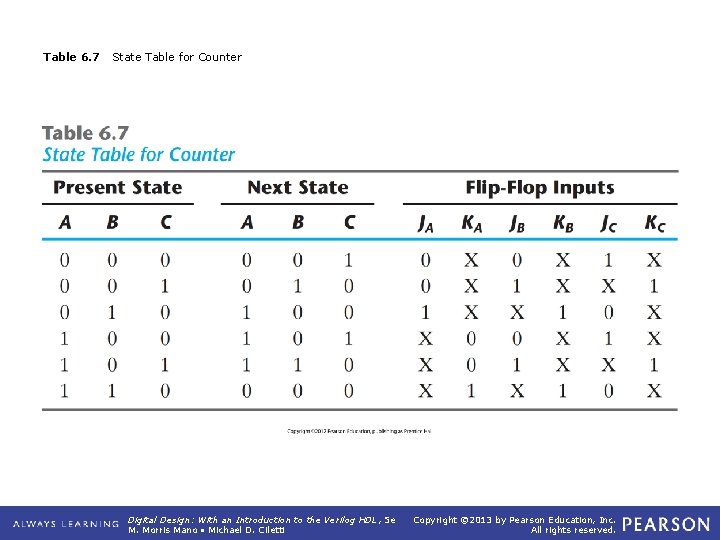
Table 6. 7 State Table for Counter Digital Design: With an Introduction to the Verilog HDL, 5 e M. Morris Mano • Michael D. Ciletti Copyright © 2013 by Pearson Education, Inc. All rights reserved.
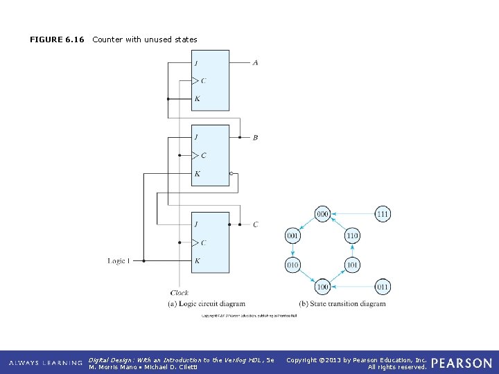
FIGURE 6. 16 Counter with unused states Digital Design: With an Introduction to the Verilog HDL, 5 e M. Morris Mano • Michael D. Ciletti Copyright © 2013 by Pearson Education, Inc. All rights reserved.
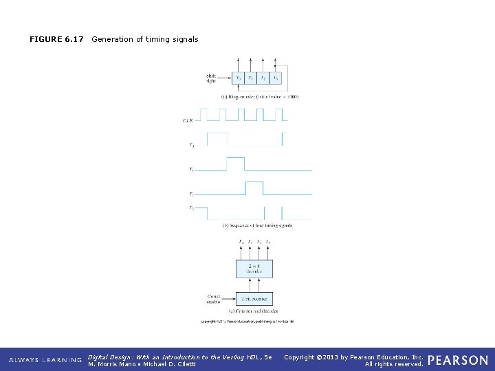
FIGURE 6. 17 Generation of timing signals Digital Design: With an Introduction to the Verilog HDL, 5 e M. Morris Mano • Michael D. Ciletti Copyright © 2013 by Pearson Education, Inc. All rights reserved.
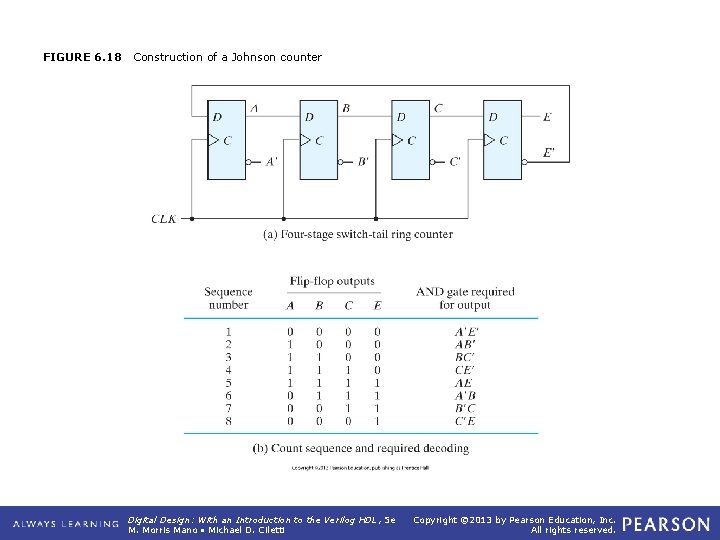
FIGURE 6. 18 Construction of a Johnson counter Digital Design: With an Introduction to the Verilog HDL, 5 e M. Morris Mano • Michael D. Ciletti Copyright © 2013 by Pearson Education, Inc. All rights reserved.
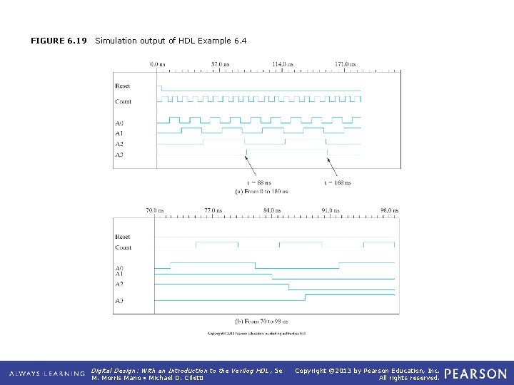
FIGURE 6. 19 Simulation output of HDL Example 6. 4 Digital Design: With an Introduction to the Verilog HDL, 5 e M. Morris Mano • Michael D. Ciletti Copyright © 2013 by Pearson Education, Inc. All rights reserved.
- Slides: 26