Figure 10 29 The memory bank write selection
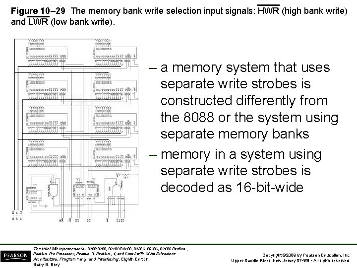
Figure 10– 29 The memory bank write selection input signals: HWR (high bank write) and LWR (low bank write). – a memory system that uses separate write strobes is constructed differently from the 8088 or the system using separate memory banks – memory in a system using separate write strobes is decoded as 16 -bit-wide The Intel Microprocessors: 8086/8088, 80186/80188, 80286, 80386, 80486 Pentium, Pentium Processor, Pentium II, Pentium, 4, and Core 2 with 64 -bit Extensions Architecture, Programming, and Interfacing, Eighth Edition Barry B. Brey Copyright © 2009 by Pearson Education, Inc. Upper Saddle River, New Jersey 07458 • All rights reserved.
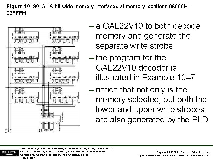
Figure 10– 30 A 16 -bit-wide memory interfaced at memory locations 06000 H– 06 FFFH. – a GAL 22 V 10 to both decode memory and generate the separate write strobe – the program for the GAL 22 V 10 decoder is illustrated in Example 10– 7 – notice that not only is the memory selected, but both the lower and upper write strobes are also generated by the PLD The Intel Microprocessors: 8086/8088, 80186/80188, 80286, 80386, 80486 Pentium, Pentium Processor, Pentium II, Pentium, 4, and Core 2 with 64 -bit Extensions Architecture, Programming, and Interfacing, Eighth Edition Barry B. Brey Copyright © 2009 by Pearson Education, Inc. Upper Saddle River, New Jersey 07458 • All rights reserved.
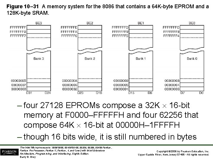
Figure 10– 31 A memory system for the 8086 that contains a 64 K-byte EPROM and a 128 K-byte SRAM. – four 27128 EPROMs compose a 32 K 16 -bit memory at F 0000–FFFFFH and four 62256 that compose 64 K 16 -bit at 00000 H– 1 FFFFH – though 16 bits wide, it is still numbered in bytes The Intel Microprocessors: 8086/8088, 80186/80188, 80286, 80386, 80486 Pentium, Pentium Processor, Pentium II, Pentium, 4, and Core 2 with 64 -bit Extensions Architecture, Programming, and Interfacing, Eighth Edition Barry B. Brey Copyright © 2009 by Pearson Education, Inc. Upper Saddle River, New Jersey 07458 • All rights reserved.
• Fig 10– 32 shows a memory connected to an 80386 SX by using a GAL 22 V 10 as a decoder. • This interface contains 256 K bytes of EPROM in the form of four 27512 (64 K 8) EPROMs and 128 K bytes of SRAM memory found in four 62256 (32 K 8) SRAMs. • The PLD decodes the 16 -bit-wide memory addresses at locations 000000 H– 01 FFFFH for the SRAM and locations FC 0000 H– FFFFFFH for the EPROM. The Intel Microprocessors: 8086/8088, 80186/80188, 80286, 80386, 80486 Pentium, Pentium Processor, Pentium II, Pentium, 4, and Core 2 with 64 -bit Extensions Architecture, Programming, and Interfacing, Eighth Edition Barry B. Brey Copyright © 2009 by Pearson Education, Inc. Upper Saddle River, New Jersey 07458 • All rights reserved.
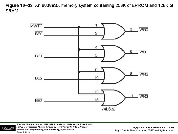
Figure 10– 32 An 80386 SX memory system containing 256 K of EPROM and 128 K of SRAM. The Intel Microprocessors: 8086/8088, 80186/80188, 80286, 80386, 80486 Pentium, Pentium Processor, Pentium II, Pentium, 4, and Core 2 with 64 -bit Extensions Architecture, Programming, and Interfacing, Eighth Edition Barry B. Brey Copyright © 2009 by Pearson Education, Inc. Upper Saddle River, New Jersey 07458 • All rights reserved.
10– 5 80386 DX and 80486 (32 -Bit) MEMORY INTERFACE • A 32 -bit memory system has a 32 -bit data bus and four banks of memory. • Both 80386 DX and 80486 (SX and DX) contain a 32 -bit address bus that usually requires PLD decoders instead of integrated decoders. – because of the sizable number of address bits The Intel Microprocessors: 8086/8088, 80186/80188, 80286, 80386, 80486 Pentium, Pentium Processor, Pentium II, Pentium, 4, and Core 2 with 64 -bit Extensions Architecture, Programming, and Interfacing, Eighth Edition Barry B. Brey Copyright © 2009 by Pearson Education, Inc. Upper Saddle River, New Jersey 07458 • All rights reserved.
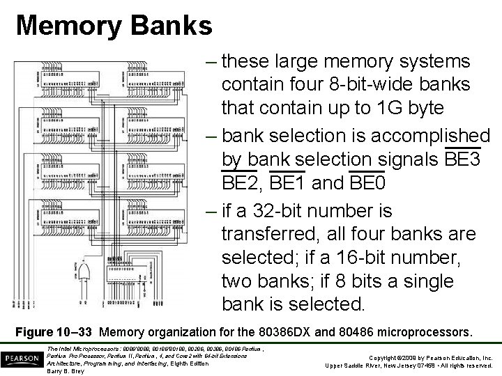
Memory Banks – these large memory systems contain four 8 -bit-wide banks that contain up to 1 G byte – bank selection is accomplished by bank selection signals BE 3 BE 2, BE 1 and BE 0 – if a 32 -bit number is transferred, all four banks are selected; if a 16 -bit number, two banks; if 8 bits a single bank is selected. Figure 10– 33 Memory organization for the 80386 DX and 80486 microprocessors. The Intel Microprocessors: 8086/8088, 80186/80188, 80286, 80386, 80486 Pentium, Pentium Processor, Pentium II, Pentium, 4, and Core 2 with 64 -bit Extensions Architecture, Programming, and Interfacing, Eighth Edition Barry B. Brey Copyright © 2009 by Pearson Education, Inc. Upper Saddle River, New Jersey 07458 • All rights reserved.
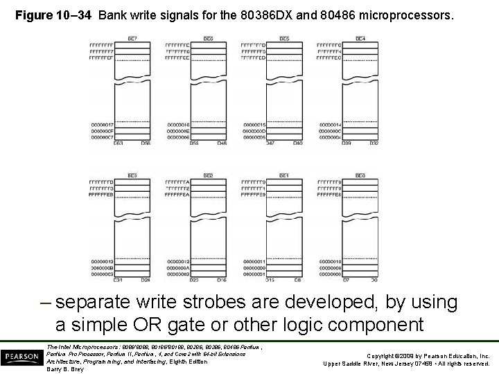
Figure 10– 34 Bank write signals for the 80386 DX and 80486 microprocessors. – separate write strobes are developed, by using a simple OR gate or other logic component The Intel Microprocessors: 8086/8088, 80186/80188, 80286, 80386, 80486 Pentium, Pentium Processor, Pentium II, Pentium, 4, and Core 2 with 64 -bit Extensions Architecture, Programming, and Interfacing, Eighth Edition Barry B. Brey Copyright © 2009 by Pearson Education, Inc. Upper Saddle River, New Jersey 07458 • All rights reserved.
32 -Bit Memory Interface • A memory interface for 80386 DX or 80486 requires four bank write strobes and decoding a 32 -bit address. – there are no integrated decoders, such as the 74 LS 138, that can easily accommodate a memory interface for the 80386 DX or 80486 • Figure 10– 35 shows a 512 K 8 SRAM memory system for the 80486. – This uses eight 64 K 8 SRAM memory devices, a PLD, and an OR gate The Intel Microprocessors: 8086/8088, 80186/80188, 80286, 80386, 80486 Pentium, Pentium Processor, Pentium II, Pentium, 4, and Core 2 with 64 -bit Extensions Architecture, Programming, and Interfacing, Eighth Edition Barry B. Brey Copyright © 2009 by Pearson Education, Inc. Upper Saddle River, New Jersey 07458 • All rights reserved.
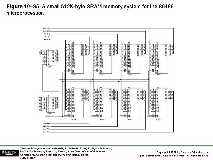
Figure 10– 35 A small 512 K-byte SRAM memory system for the 80486 microprocessor. The Intel Microprocessors: 8086/8088, 80186/80188, 80286, 80386, 80486 Pentium, Pentium Processor, Pentium II, Pentium, 4, and Core 2 with 64 -bit Extensions Architecture, Programming, and Interfacing, Eighth Edition Barry B. Brey Copyright © 2009 by Pearson Education, Inc. Upper Saddle River, New Jersey 07458 • All rights reserved.
• 80386 DX and 80486 microprocessors operate with very high clock rates. – usually require wait states for memory access • The interface provides a signal used with the wait state generator. • Other devices with these higher speed microprocessors are cache memory and interleaved memory systems. The Intel Microprocessors: 8086/8088, 80186/80188, 80286, 80386, 80486 Pentium, Pentium Processor, Pentium II, Pentium, 4, and Core 2 with 64 -bit Extensions Architecture, Programming, and Interfacing, Eighth Edition Barry B. Brey Copyright © 2009 by Pearson Education, Inc. Upper Saddle River, New Jersey 07458 • All rights reserved.
10– 6 PENTIUM THROUGH CORE 2 (64 -Bit) MEMORY INTERFACE • The Pentium - Core 2 contain a 64 -bit data bus, which requires eight decoders (one per bank) or eight separate write signals. – except the P 24 T version of the Pentium • In most systems, separate write signals are used when interfacing memory. • Figure 10– 36 shows the Pentium memory organization and its eight memory banks. The Intel Microprocessors: 8086/8088, 80186/80188, 80286, 80386, 80486 Pentium, Pentium Processor, Pentium II, Pentium, 4, and Core 2 with 64 -bit Extensions Architecture, Programming, and Interfacing, Eighth Edition Barry B. Brey Copyright © 2009 by Pearson Education, Inc. Upper Saddle River, New Jersey 07458 • All rights reserved.
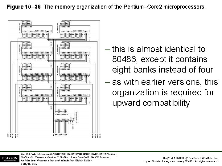
Figure 10– 36 The memory organization of the Pentium–Core 2 microprocessors. – this is almost identical to 80486, except it contains eight banks instead of four – as with earlier versions, this organization is required for upward compatibility The Intel Microprocessors: 8086/8088, 80186/80188, 80286, 80386, 80486 Pentium, Pentium Processor, Pentium II, Pentium, 4, and Core 2 with 64 -bit Extensions Architecture, Programming, and Interfacing, Eighth Edition Barry B. Brey Copyright © 2009 by Pearson Education, Inc. Upper Saddle River, New Jersey 07458 • All rights reserved.
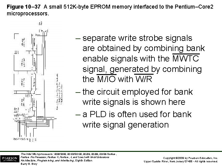
Figure 10– 37 A small 512 K-byte EPROM memory interfaced to the Pentium–Core 2 microprocessors. – separate write strobe signals are obtained by combining bank enable signals with the MWTC signal, generated by combining the M/IO with W/R – the circuit employed for bank write signals is shown here – a PLD is often used for bank write signal generation The Intel Microprocessors: 8086/8088, 80186/80188, 80286, 80386, 80486 Pentium, Pentium Processor, Pentium II, Pentium, 4, and Core 2 with 64 -bit Extensions Architecture, Programming, and Interfacing, Eighth Edition Barry B. Brey Copyright © 2009 by Pearson Education, Inc. Upper Saddle River, New Jersey 07458 • All rights reserved.
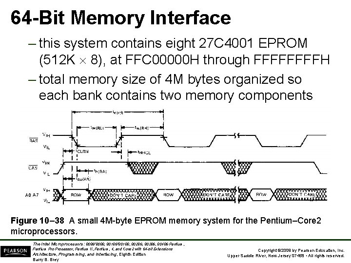
64 -Bit Memory Interface – this system contains eight 27 C 4001 EPROM (512 K 8), at FFC 00000 H through FFFFH – total memory size of 4 M bytes organized so each bank contains two memory components Figure 10– 38 A small 4 M-byte EPROM memory system for the Pentium–Core 2 microprocessors. The Intel Microprocessors: 8086/8088, 80186/80188, 80286, 80386, 80486 Pentium, Pentium Processor, Pentium II, Pentium, 4, and Core 2 with 64 -bit Extensions Architecture, Programming, and Interfacing, Eighth Edition Barry B. Brey Copyright © 2009 by Pearson Education, Inc. Upper Saddle River, New Jersey 07458 • All rights reserved.
10– 7 DYNAMIC RAM • Because RAM is often large, it requires many SRAMs at great cost or a few DRAMs (dynamic RAMs) at much reduced cost. • IC manufacturers have provided a dynamic RAM controller with address multiplexers and timing circuitry necessary for refreshing. • This section of the text covers the DRAM and provides information on the use of a dynamic controller in a memory system. The Intel Microprocessors: 8086/8088, 80186/80188, 80286, 80386, 80486 Pentium, Pentium Processor, Pentium II, Pentium, 4, and Core 2 with 64 -bit Extensions Architecture, Programming, and Interfacing, Eighth Edition Barry B. Brey Copyright © 2009 by Pearson Education, Inc. Upper Saddle River, New Jersey 07458 • All rights reserved.
DRAM Revisited • DRAM must be refreshed periodically as it stores data internally on capacitors that lose charge in a short period of time. – to refresh DRAM, contents of a section of the memory must periodically be read or written • Any read or write automatically refreshes an entire section of the DRAM. • The number of bits refreshed depends on the size of the memory component and its internal organization. The Intel Microprocessors: 8086/8088, 80186/80188, 80286, 80386, 80486 Pentium, Pentium Processor, Pentium II, Pentium, 4, and Core 2 with 64 -bit Extensions Architecture, Programming, and Interfacing, Eighth Edition Barry B. Brey Copyright © 2009 by Pearson Education, Inc. Upper Saddle River, New Jersey 07458 • All rights reserved.
• Refresh cycles are done with a read, write, or a special refresh that doesn’t read or write. • The refresh cycle is internal to the DRAM and often accomplished while other memory components in the system operate. – this is called hidden refresh, transparent refresh, or sometimes, cycle stealing • To do a hidden refresh while other memory components are functioning, an RAS -only cycle strobes a row address into the DRAM to select a row of bits to be refreshed. The Intel Microprocessors: 8086/8088, 80186/80188, 80286, 80386, 80486 Pentium, Pentium Processor, Pentium II, Pentium, 4, and Core 2 with 64 -bit Extensions Architecture, Programming, and Interfacing, Eighth Edition Barry B. Brey Copyright © 2009 by Pearson Education, Inc. Upper Saddle River, New Jersey 07458 • All rights reserved.
• The RAS input also causes the selected row to be read and rewritten into the selected bits. – this recharges internal capacitors that store data • This refresh is hidden from the system because it occurs while the processor is reading or writing other sections of memory The Intel Microprocessors: 8086/8088, 80186/80188, 80286, 80386, 80486 Pentium, Pentium Processor, Pentium II, Pentium, 4, and Core 2 with 64 -bit Extensions Architecture, Programming, and Interfacing, Eighth Edition Barry B. Brey Copyright © 2009 by Pearson Education, Inc. Upper Saddle River, New Jersey 07458 • All rights reserved.
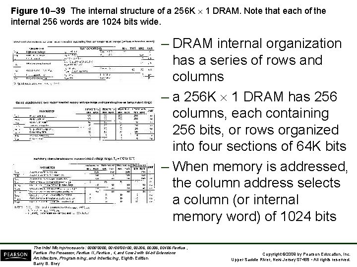
Figure 10– 39 The internal structure of a 256 K 1 DRAM. Note that each of the internal 256 words are 1024 bits wide. – DRAM internal organization has a series of rows and columns – a 256 K 1 DRAM has 256 columns, each containing 256 bits, or rows organized into four sections of 64 K bits – When memory is addressed, the column address selects a column (or internal memory word) of 1024 bits The Intel Microprocessors: 8086/8088, 80186/80188, 80286, 80386, 80486 Pentium, Pentium Processor, Pentium II, Pentium, 4, and Core 2 with 64 -bit Extensions Architecture, Programming, and Interfacing, Eighth Edition Barry B. Brey Copyright © 2009 by Pearson Education, Inc. Upper Saddle River, New Jersey 07458 • All rights reserved.
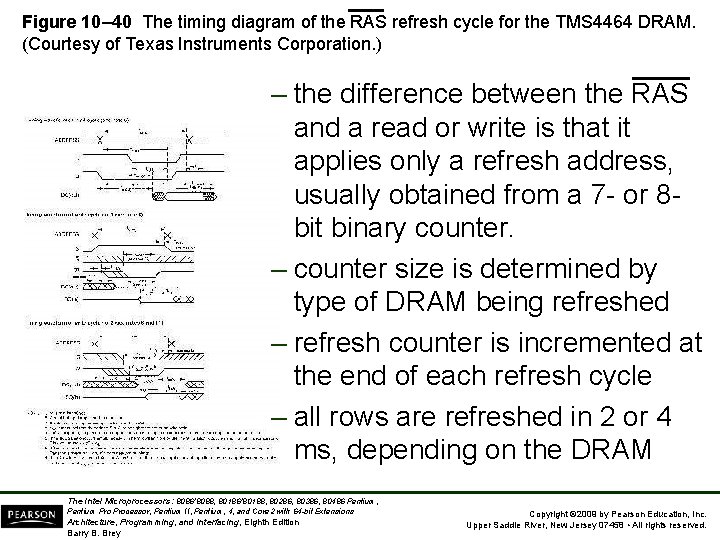
Figure 10– 40 The timing diagram of the RAS refresh cycle for the TMS 4464 DRAM. (Courtesy of Texas Instruments Corporation. ) – the difference between the RAS and a read or write is that it applies only a refresh address, usually obtained from a 7 - or 8 bit binary counter. – counter size is determined by type of DRAM being refreshed – refresh counter is incremented at the end of each refresh cycle – all rows are refreshed in 2 or 4 ms, depending on the DRAM The Intel Microprocessors: 8086/8088, 80186/80188, 80286, 80386, 80486 Pentium, Pentium Processor, Pentium II, Pentium, 4, and Core 2 with 64 -bit Extensions Architecture, Programming, and Interfacing, Eighth Edition Barry B. Brey Copyright © 2009 by Pearson Education, Inc. Upper Saddle River, New Jersey 07458 • All rights reserved.
• If there are 256 rows to be refreshed within 4 ms, the refresh cycle must be activated at least once every 15. 6 µs. – in a modern system such as a 3. 0 GHz Pentium 4, 15. 6 µs is a great deal of time • Since the 3. 0 GHz Pentium 4 executes an instruction in about one-third ns, it can execute about 46, 000 instructions between refreshes. • In new machines much less than 1% ( 0. 002 %) is required for a refresh. The Intel Microprocessors: 8086/8088, 80186/80188, 80286, 80386, 80486 Pentium, Pentium Processor, Pentium II, Pentium, 4, and Core 2 with 64 -bit Extensions Architecture, Programming, and Interfacing, Eighth Edition Barry B. Brey Copyright © 2009 by Pearson Education, Inc. Upper Saddle River, New Jersey 07458 • All rights reserved.
EDO Memory • Slight modification to the DRAM changes it an EDO (extended data output) DRAM device. • In EDO memory, any memory access, including a refresh, stores the 256 bits selected by RAS into latches. • This slight modification increases system performance by about 15% to 25%. • Although EDO memory is no longer available, the technique is employed in modern DRAM. The Intel Microprocessors: 8086/8088, 80186/80188, 80286, 80386, 80486 Pentium, Pentium Processor, Pentium II, Pentium, 4, and Core 2 with 64 -bit Extensions Architecture, Programming, and Interfacing, Eighth Edition Barry B. Brey Copyright © 2009 by Pearson Education, Inc. Upper Saddle River, New Jersey 07458 • All rights reserved.
SDRAM • Synchronous dynamic RAM (SDRAM) is used with most newer systems because of speed. • Versions are available with access times as low as 7 ns, for the 133 MHz bus. • When a burst transfer occurs to the SDRAM from the processor, it takes three or four bus clocks before the first 64 -bit number is read. • Each subsequent number is read without wait states and in one bus cycle each. The Intel Microprocessors: 8086/8088, 80186/80188, 80286, 80386, 80486 Pentium, Pentium Processor, Pentium II, Pentium, 4, and Core 2 with 64 -bit Extensions Architecture, Programming, and Interfacing, Eighth Edition Barry B. Brey Copyright © 2009 by Pearson Education, Inc. Upper Saddle River, New Jersey 07458 • All rights reserved.
• Because SDRAM bursts read four 64 -bit numbers, the second through fourth require no waits, and can be read in one bus cycle each, SDRAM outperforms standard DRAM. • Most estimates place SDRAM at about a 10% performance increase over EDO memory. The Intel Microprocessors: 8086/8088, 80186/80188, 80286, 80386, 80486 Pentium, Pentium Processor, Pentium II, Pentium, 4, and Core 2 with 64 -bit Extensions Architecture, Programming, and Interfacing, Eighth Edition Barry B. Brey Copyright © 2009 by Pearson Education, Inc. Upper Saddle River, New Jersey 07458 • All rights reserved.
DDR • Double-data rate (DDR) memory is the latest improvement in DRAM modifications. – DDR memory data at double SDRAM speed because it transfers on each edge of the clock – the positive edge is used for a transfer and so is the negative edge • Even though this seems as if it doubles the speed of the memory, it really does not. – access time problems still exist, with even most advanced memory requiring access time of 40 ns. The Intel Microprocessors: 8086/8088, 80186/80188, 80286, 80386, 80486 Pentium, Pentium Processor, Pentium II, Pentium, 4, and Core 2 with 64 -bit Extensions Architecture, Programming, and Interfacing, Eighth Edition Barry B. Brey Copyright © 2009 by Pearson Education, Inc. Upper Saddle River, New Jersey 07458 • All rights reserved.
DRAM Controllers • In most systems, a DRAM controller-IC performs address multiplexing and generation of the DRAM control signals. – newer embedded processors, such as 80186/8, include refresh circuitry as part of the processor • Most modern computers contain the DRAM controller in the chip set so a stand-alone DRAM controller is not available. The Intel Microprocessors: 8086/8088, 80186/80188, 80286, 80386, 80486 Pentium, Pentium Processor, Pentium II, Pentium, 4, and Core 2 with 64 -bit Extensions Architecture, Programming, and Interfacing, Eighth Edition Barry B. Brey Copyright © 2009 by Pearson Education, Inc. Upper Saddle River, New Jersey 07458 • All rights reserved.
• The DRAM controller in the chip set for the microprocessor times refresh cycles and inserts refresh cycles into the timing. • The memory refresh is transparent to the microprocessor, because it really does not control refreshing. • For Pentium II, III, and P 4, DRAM control is built in the chip set provided by Intel or AMD. • In the future, even the chip set will undoubtedly be built into the microprocessor. The Intel Microprocessors: 8086/8088, 80186/80188, 80286, 80386, 80486 Pentium, Pentium Processor, Pentium II, Pentium, 4, and Core 2 with 64 -bit Extensions Architecture, Programming, and Interfacing, Eighth Edition Barry B. Brey Copyright © 2009 by Pearson Education, Inc. Upper Saddle River, New Jersey 07458 • All rights reserved.
- Slides: 28