Field Effect Transistors Session 6 a for Electronics
- Slides: 17

Field Effect Transistors Session 6 a for Electronics and Telecommunications A Fairfield University E-Course Powered by Learn. Linc 10/22/2021 Electronics and Telecommunications 1

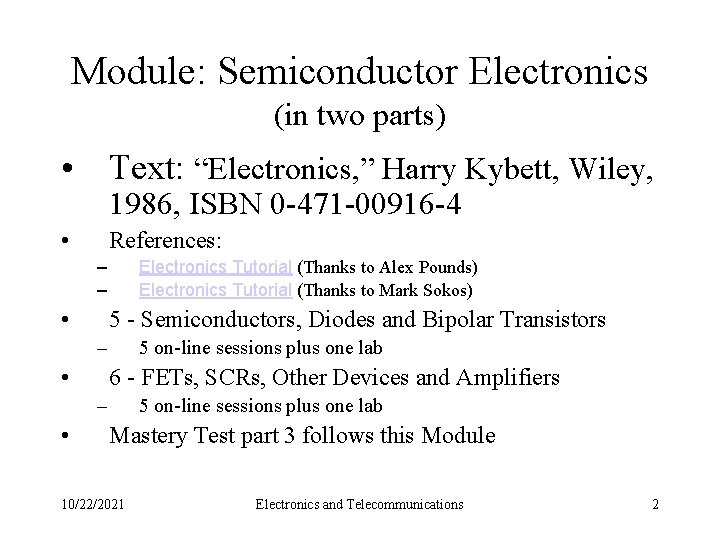
Module: Semiconductor Electronics (in two parts) • Text: “Electronics, ” Harry Kybett, Wiley, 1986, ISBN 0 -471 -00916 -4 • References: – – • Electronics Tutorial (Thanks to Alex Pounds) Electronics Tutorial (Thanks to Mark Sokos) 5 - Semiconductors, Diodes and Bipolar Transistors – • 5 on-line sessions plus one lab 6 - FETs, SCRs, Other Devices and Amplifiers – • 5 on-line sessions plus one lab Mastery Test part 3 follows this Module 10/22/2021 Electronics and Telecommunications 2

Section 6: FETs, SCRs, Other Devices and Operational Amplifiers • 0 BJECTIVES: This section reviews additional important semiconductor devices and their applications. The Operational Amplifier is also studied. 10/22/2021 Electronics and Telecommunications 3

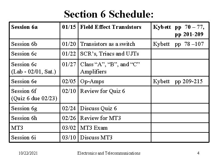
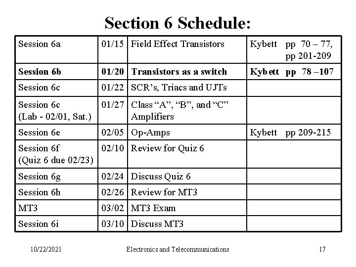
Section 6 Schedule: Session 6 a 01/15 Field Effect Transistors Kybett pp 70 – 77, pp 201 -209 Session 6 b 01/20 Transistors as a switch Kybett pp 78 – 107 Session 6 c 01/22 SCR’s, Triacs and UJTs Session 6 c (Lab - 02/01, Sat. ) 01/27 Class “A”, “B”, and “C” Amplifiers Session 6 e 02/05 Op-Amps Kybett pp 209 -215 Session 6 f 02/10 Review for Quiz 6 (Quiz 6 due 02/23) Session 6 g 02/24 Discuss Quiz 6 Session 6 h 02/26 Review for MT 3 03/02 MT 3 Exam Session 6 i 03/10 Discuss MT 3 10/22/2021 Electronics and Telecommunications 4

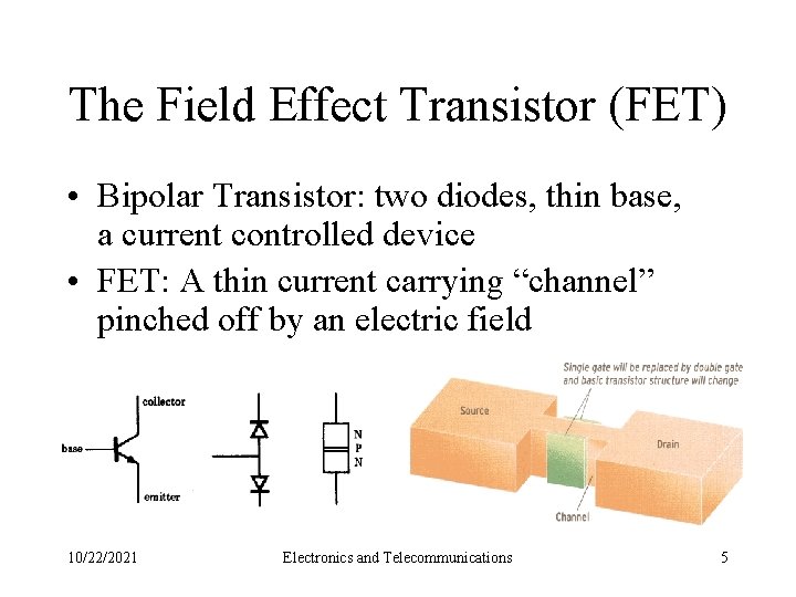
The Field Effect Transistor (FET) • Bipolar Transistor: two diodes, thin base, a current controlled device • FET: A thin current carrying “channel” pinched off by an electric field 10/22/2021 Electronics and Telecommunications 5

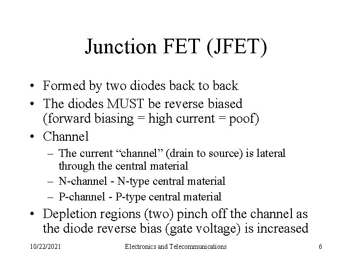
Junction FET (JFET) • Formed by two diodes back to back • The diodes MUST be reverse biased (forward biasing = high current = poof) • Channel – The current “channel” (drain to source) is lateral through the central material – N-channel - N-type central material – P-channel - P-type central material • Depletion regions (two) pinch off the channel as the diode reverse bias (gate voltage) is increased 10/22/2021 Electronics and Telecommunications 6

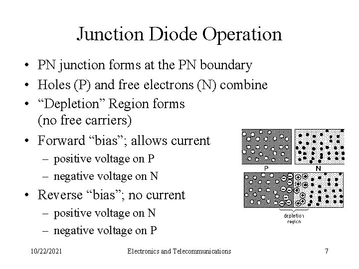
Junction Diode Operation • PN junction forms at the PN boundary • Holes (P) and free electrons (N) combine • “Depletion” Region forms (no free carriers) • Forward “bias”; allows current – positive voltage on P – negative voltage on N • Reverse “bias”; no current – positive voltage on N – negative voltage on P 10/22/2021 Electronics and Telecommunications 7

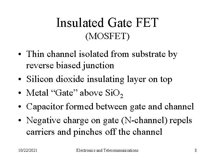
Insulated Gate FET (MOSFET) • Thin channel isolated from substrate by reverse biased junction • Silicon dioxide insulating layer on top • Metal “Gate” above Si. O 2 • Capacitor formed between gate and channel • Negative charge on gate (N-channel) repels carriers and pinches off the channel 10/22/2021 Electronics and Telecommunications 8

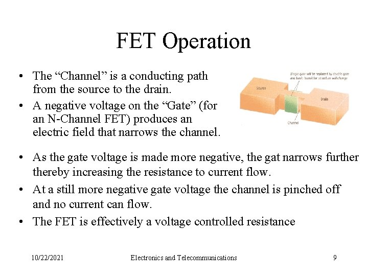
FET Operation • The “Channel” is a conducting path from the source to the drain. • A negative voltage on the “Gate” (for an N-Channel FET) produces an electric field that narrows the channel. • As the gate voltage is made more negative, the gat narrows furthereby increasing the resistance to current flow. • At a still more negative gate voltage the channel is pinched off and no current can flow. • The FET is effectively a voltage controlled resistance 10/22/2021 Electronics and Telecommunications 9

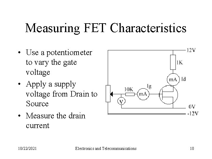
Measuring FET Characteristics • Use a potentiometer to vary the gate voltage • Apply a supply voltage from Drain to Source • Measure the drain current 10/22/2021 Electronics and Telecommunications 10

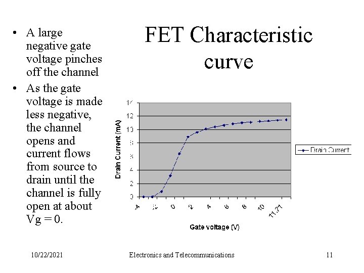
• A large negative gate voltage pinches off the channel • As the gate voltage is made less negative, the channel opens and current flows from source to drain until the channel is fully open at about Vg = 0. 10/22/2021 FET Characteristic curve Electronics and Telecommunications 11

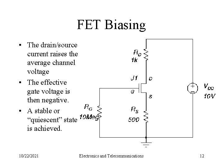
FET Biasing • The drain/source current raises the average channel voltage • The effective gate voltage is then negative. • A stable or “quiescent” state is achieved. 10/22/2021 Electronics and Telecommunications 12

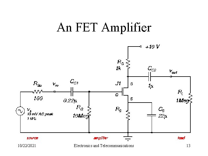
An FET Amplifier 10/22/2021 Electronics and Telecommunications 13

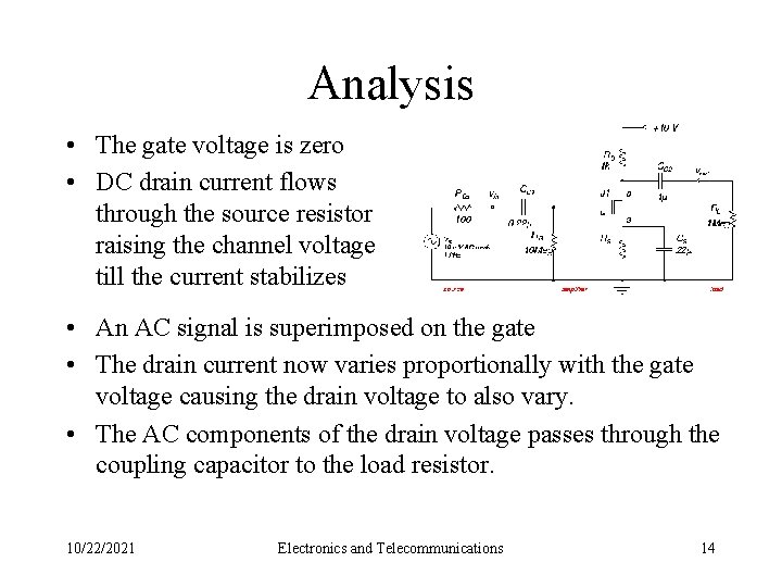
Analysis • The gate voltage is zero • DC drain current flows through the source resistor raising the channel voltage till the current stabilizes • An AC signal is superimposed on the gate • The drain current now varies proportionally with the gate voltage causing the drain voltage to also vary. • The AC components of the drain voltage passes through the coupling capacitor to the load resistor. 10/22/2021 Electronics and Telecommunications 14

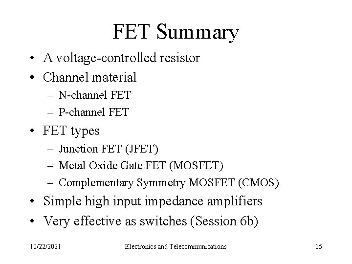
FET Summary • A voltage-controlled resistor • Channel material – N-channel FET – P-channel FET • FET types – Junction FET (JFET) – Metal Oxide Gate FET (MOSFET) – Complementary Symmetry MOSFET (CMOS) • Simple high input impedance amplifiers • Very effective as switches (Session 6 b) 10/22/2021 Electronics and Telecommunications 15

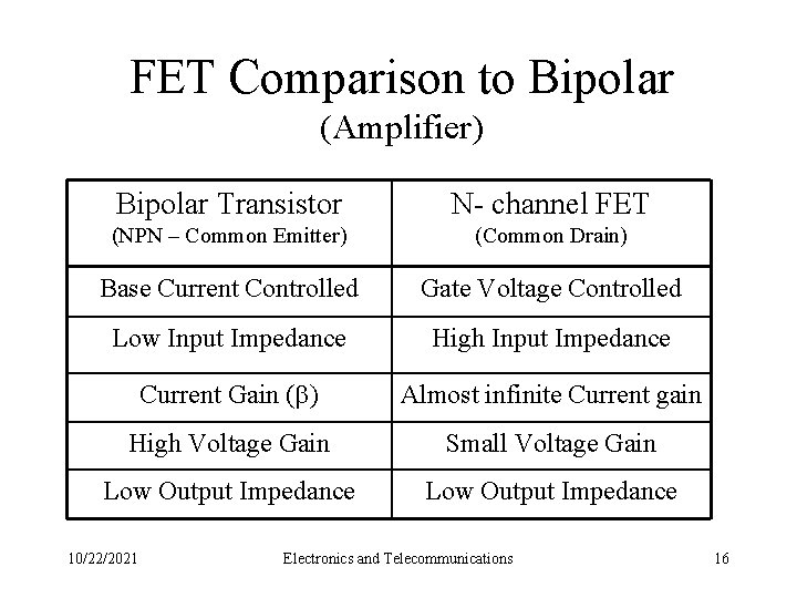
FET Comparison to Bipolar (Amplifier) Bipolar Transistor N- channel FET (NPN – Common Emitter) (Common Drain) Base Current Controlled Gate Voltage Controlled Low Input Impedance High Input Impedance Current Gain ( ) Almost infinite Current gain High Voltage Gain Small Voltage Gain Low Output Impedance 10/22/2021 Electronics and Telecommunications 16

Section 6 Schedule: Session 6 a 01/15 Field Effect Transistors Kybett pp 70 – 77, pp 201 -209 Session 6 b 01/20 Transistors as a switch Kybett pp 78 – 107 Session 6 c 01/22 SCR’s, Triacs and UJTs Session 6 c (Lab - 02/01, Sat. ) 01/27 Class “A”, “B”, and “C” Amplifiers Session 6 e 02/05 Op-Amps Kybett pp 209 -215 Session 6 f 02/10 Review for Quiz 6 (Quiz 6 due 02/23) Session 6 g 02/24 Discuss Quiz 6 Session 6 h 02/26 Review for MT 3 03/02 MT 3 Exam Session 6 i 03/10 Discuss MT 3 10/22/2021 Electronics and Telecommunications 17