Ferromagnetic semiconductors for spintronics Theory concepts and experimental
![Devices utilizing M-dependent electro-chemical potentials: FM SET [110] [010] M Drain Gate VG [100] Devices utilizing M-dependent electro-chemical potentials: FM SET [110] [010] M Drain Gate VG [100]](https://slidetodoc.com/presentation_image/e7e376142b50a311c08001c32446c80d/image-23.jpg)
![SO-coupling (M) (Ga, Mn)As nano-constriction SET M [ 010 ] [110] [100] [110] [010] SO-coupling (M) (Ga, Mn)As nano-constriction SET M [ 010 ] [110] [100] [110] [010]](https://slidetodoc.com/presentation_image/e7e376142b50a311c08001c32446c80d/image-24.jpg)
- Slides: 48

Ferromagnetic semiconductors for spintronics Theory concepts and experimental overview Tomas Jungwirth Institute of Physics ASCR Jan Mašek, Josef Kudrnovský, František Máca, Alexander Shick, Karel Výborný, Jan Zemen, Vít Novák, Kamil Olejník, et al. Hitachi Cambridge, Univ. Cambridge Jorg Wunderlich, Andrew Irvine, David Williams, Elisa de Ranieri, Byonguk Park, Sam Owen, et al. University of Nottingham Bryan Gallagher, Tom Foxon, Richard Campion, Kevin Edmonds, Andrew Rushforth, Chris King et al. Texas A&M Jairo Sinova, et al. University of Texas Allan Ma. Donald, et al.

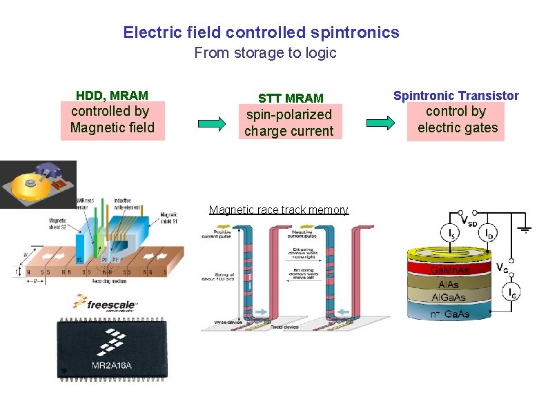
Electric field controlled spintronics From storage to logic HDD, MRAM controlled by Magnetic field STT MRAM spin-polarized charge current Magnetic race track memory Spintronic Transistor control by electric gates

Current spintronics with FM metals FM semiconductors: all features of current spintronics plus much more Basic magnetic and magnetotransport properties of (Ga, Mn)As and related FS

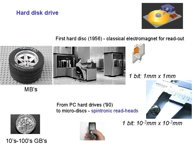
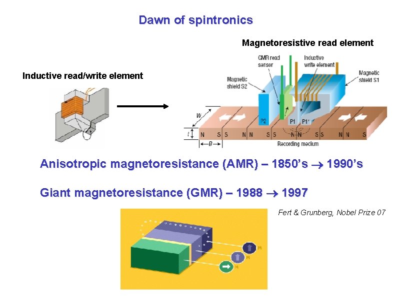
Hard disk drive First hard disc (1956) - classical electromagnet for read-out 1 bit: 1 mm x 1 mm MB’s From PC hard drives ('90) to micro-discs - spintronic read-heads 1 bit: 10 -3 mm x 10 -3 mm 10’s-100’s GB’s

Dawn of spintronics Magnetoresistive read element Inductive read/write element Anisotropic magnetoresistance (AMR) – 1850’s 1990’s Giant magnetoresistance (GMR) – 1988 1997 Fert & Grunberg, Nobel Prize 07

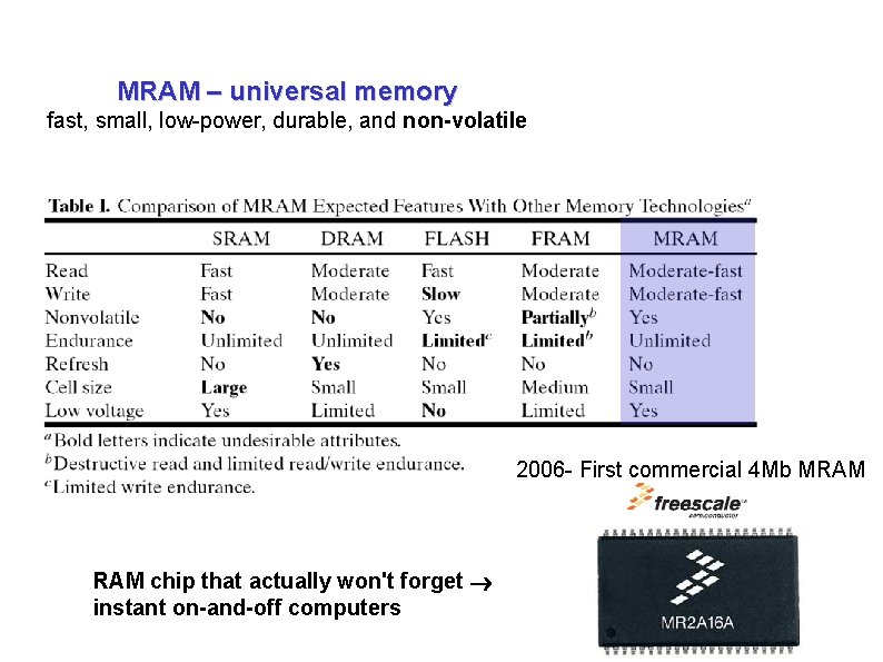
MRAM – universal memory fast, small, low-power, durable, and non-volatile 2006 - First commercial 4 Mb MRAM chip that actually won't forget instant on-and-off computers


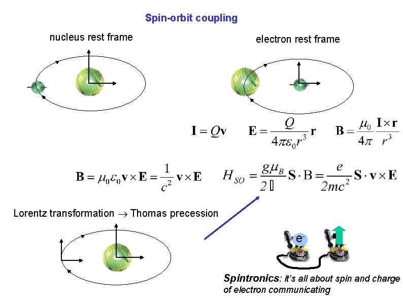
Spin-orbit coupling nucleus rest frame electron rest frame 2 2 Lorentz transformation Thomas precession e. Spintronics: it’s all about spin and charge of electron communicating

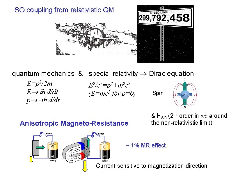
SO coupling from relativistic QM quantum mechanics & special relativity Dirac equation E=p 2/2 m E 2/c 2=p 2+m 2 c 2 E ih d/dt Spin (E=mc 2 for p=0) p -ih d/dr Anisotropic Magneto-Resistance & HSO (2 nd order in v/c around the non-relativistic limit) ~ 1% MR effect Current sensitive to magnetization direction

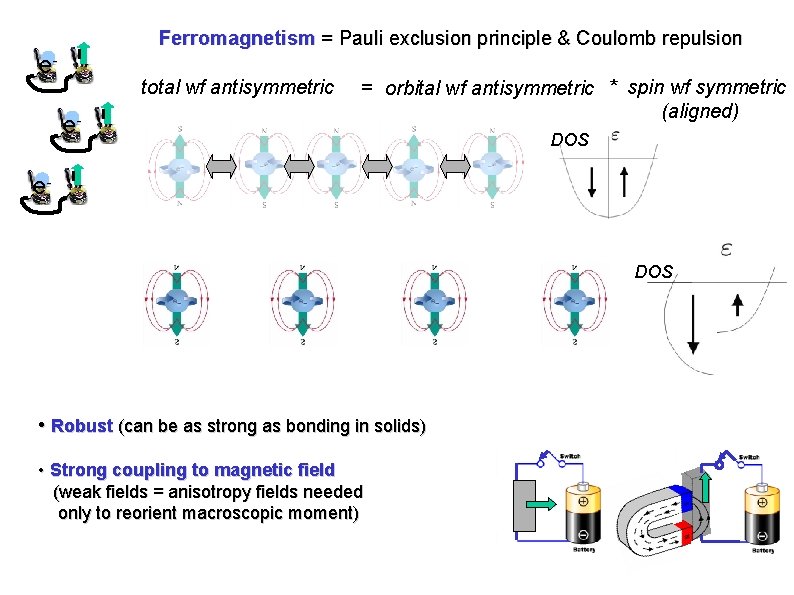
Ferromagnetism = Pauli exclusion principle & Coulomb repulsion e- total wf antisymmetric e- = orbital wf antisymmetric * spin wf symmetric (aligned) DOS e- DOS • Robust (can be as strong as bonding in solids) • Strong coupling to magnetic field (weak fields = anisotropy fields needed only to reorient macroscopic moment)

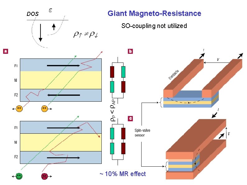
Giant Magneto-Resistance DOS SO-coupling not utilized > P AP ~ 10% MR effect

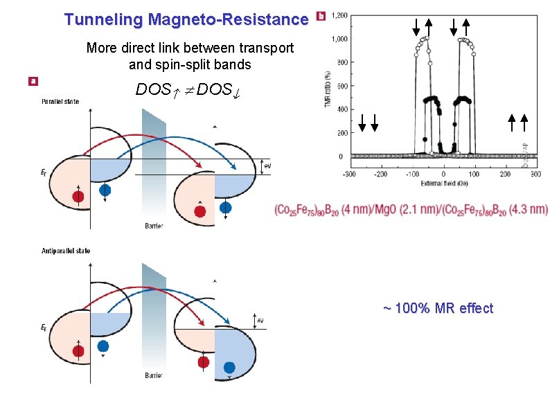
Tunneling Magneto-Resistance More direct link between transport and spin-split bands DOS ~ 100% MR effect

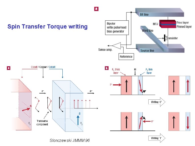
Spin Transfer Torque writing Slonczewski JMMM 96

Current spintronics with FM metals FM semiconductors: all features of current spintronics plus much more Basic magnetic and magnetotransport properties of (Ga, Mn)As and related FS

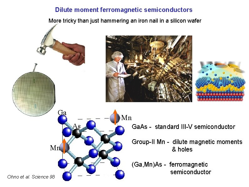
Dilute moment ferromagnetic semiconductors More tricky than just hammering an iron nail in a silicon wafer Ga Mn As Mn Ohno et al. Science 98 Ga. As - standard III-V semiconductor Group-II Mn - dilute magnetic moments & holes (Ga, Mn)As - ferromagnetic semiconductor

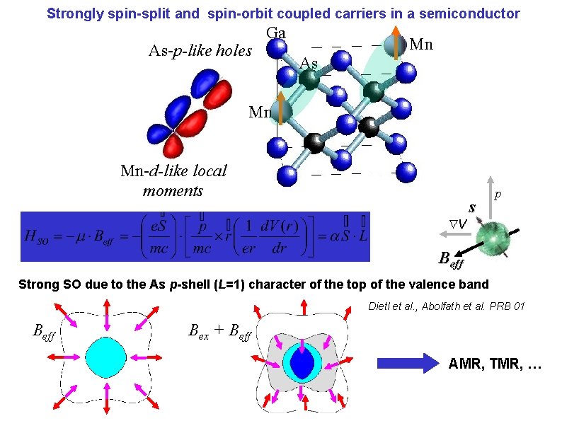
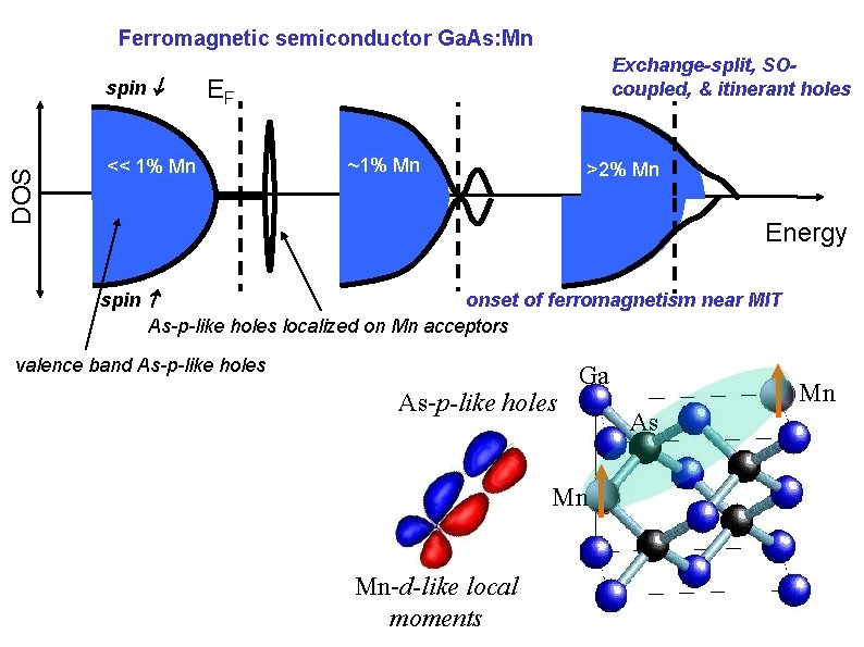
Strongly spin-split and spin-orbit coupled carriers in a semiconductor As-p-like holes Ga Mn As Mn Mn-d-like local moments V s p Beff Strong SO due to the As p-shell (L=1) character of the top of the valence band Dietl et al. , Abolfath et al. PRB 01 Beff Bex + Beff AMR, TMR, …

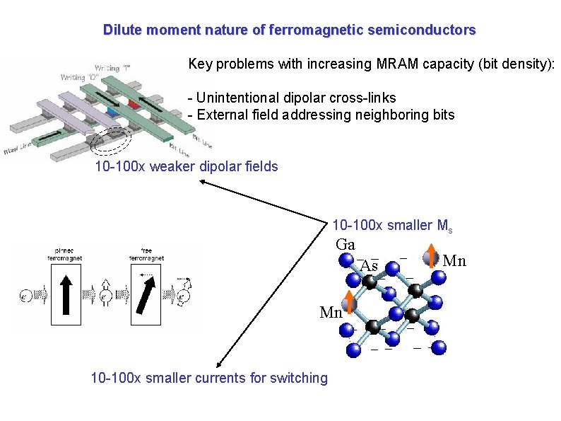
Dilute moment nature of ferromagnetic semiconductors Key problems with increasing MRAM capacity (bit density): - Unintentional dipolar cross-links - External field addressing neighboring bits One 10 -100 x weaker dipolar fields 10 -100 x smaller Ms Ga As Mn 10 -100 x smaller currents for switching Mn

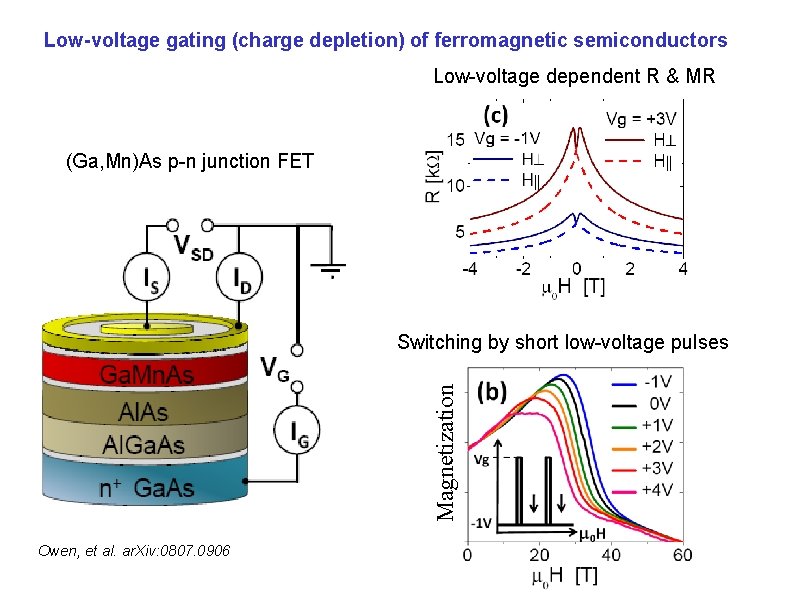
Low-voltage gating (charge depletion) of ferromagnetic semiconductors Low-voltage dependent R & MR (Ga, Mn)As p-n junction FET Magnetization Switching by short low-voltage pulses Owen, et al. ar. Xiv: 0807. 0906

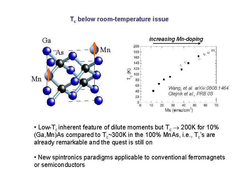
Tc below room-temperature issue increasing Mn-doping Ga As Mn Mn Wang, et al. ar. Xiv: 0808. 1464 Olejnik et al. , PRB 08 • Low-Tc inherent feature of dilute moments but Tc 200 K for 10% (Ga, Mn)As compared to Tc~300 K in the 100% Mn. As, i. e. , Tc’s are already remarkable and the quest is still on • New spintronics paradigms applicable to conventional ferromagnets or semiconductors

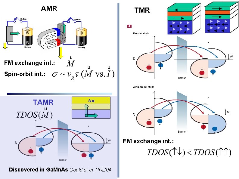
AMR TMR FM exchange int. : Spin-orbit int. : TAMR Au FM exchange int. : Discovered in Ga. Mn. As Gould et al. PRL’ 04

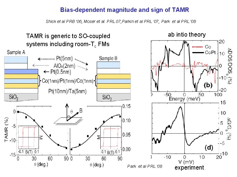
Bias-dependent magnitude and sign of TAMR Shick et al PRB ’ 06, Moser et al. PRL 07, Parkin et al PRL ‘ 07, Park et al PRL '08 ab intio theory TAMR is generic to SO-coupled systems including room-Tc FMs Park et al PRL '08 experiment

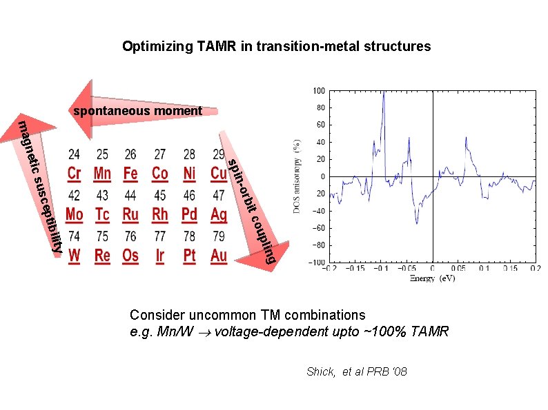
Optimizing TAMR in transition-metal structures spontaneous moment rbit cou g plin ility eptib susc n-o spi netic mag Consider uncommon TM combinations e. g. Mn/W voltage-dependent upto ~100% TAMR Shick, et al PRB ‘ 08
![Devices utilizing Mdependent electrochemical potentials FM SET 110 010 M Drain Gate VG 100 Devices utilizing M-dependent electro-chemical potentials: FM SET [110] [010] M Drain Gate VG [100]](https://slidetodoc.com/presentation_image/e7e376142b50a311c08001c32446c80d/image-23.jpg)
Devices utilizing M-dependent electro-chemical potentials: FM SET [110] [010] M Drain Gate VG [100] [110] Source Q VD [010] SO-coupling (M) electric & magnetic control of CB oscillations
![SOcoupling M Ga MnAs nanoconstriction SET M 010 110 100 110 010 SO-coupling (M) (Ga, Mn)As nano-constriction SET M [ 010 ] [110] [100] [110] [010]](https://slidetodoc.com/presentation_image/e7e376142b50a311c08001c32446c80d/image-24.jpg)
SO-coupling (M) (Ga, Mn)As nano-constriction SET M [ 010 ] [110] [100] [110] [010] ~ 1 m. V in Ga. Mn. As ~ 10 m. V in Fe. Pt Low-gate-voltage controlled huge magnitude and sign of MR very sensitive spintronic transistor Wunderlich et al, PRL '06

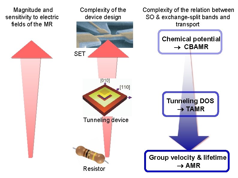
Magnitude and sensitivity to electric fields of the MR Complexity of the device design Complexity of the relation between SO & exchange-split bands and transport Chemical potential CBAMR SET Tunneling DOS TAMR Tunneling device Resistor Group velocity & lifetime AMR

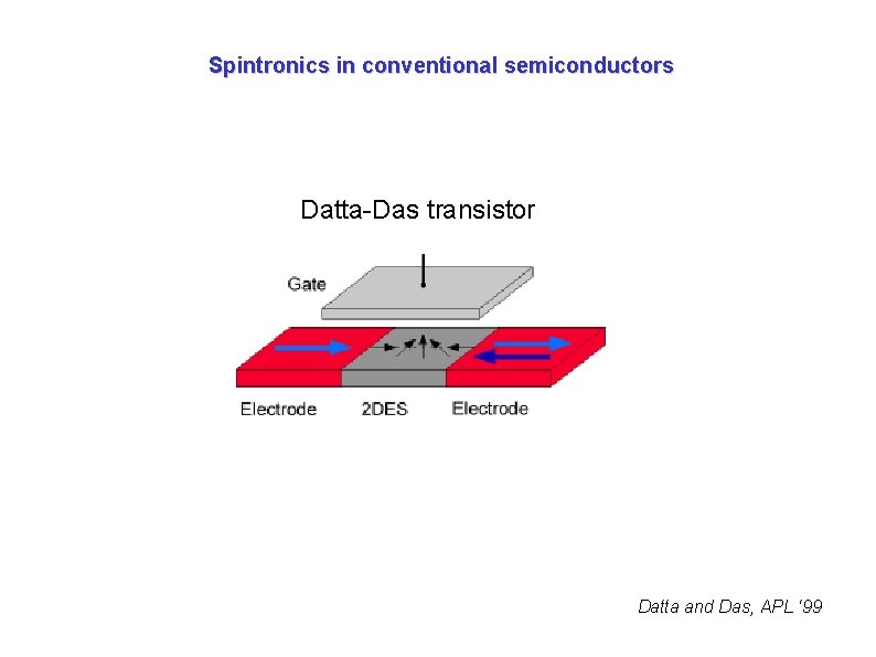
Spintronics in conventional semiconductors Datta-Das transistor Datta and Das, APL ‘ 99

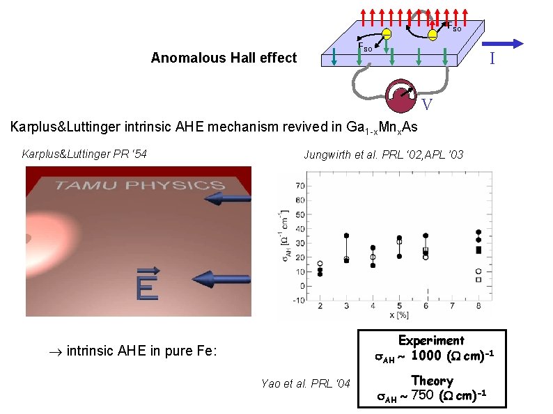
_ __ FSO Anomalous Hall effect I V Karplus&Luttinger intrinsic AHE mechanism revived in Ga 1 -x. Mnx. As Karplus&Luttinger PR ‘ 54 Jungwirth et al. PRL ‘ 02, APL ’ 03 Experiment s. AH 1000 (W cm)-1 intrinsic AHE in pure Fe: Yao et al. PRL ‘ 04 Theory s. AH 750 (W cm)-1

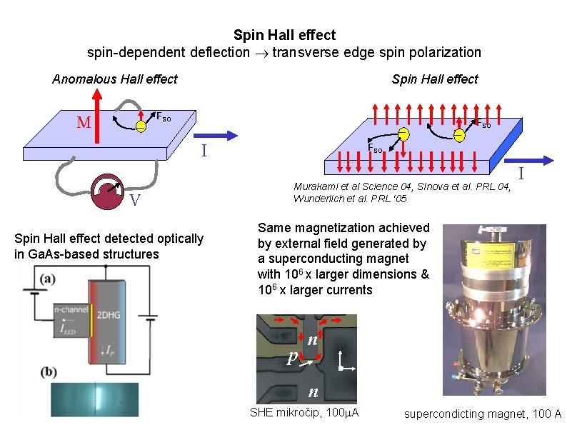
Spin Hall effect spin-dependent deflection transverse edge spin polarization Anomalous Hall effect M __ Spin Hall effect FSO _ I V Spin Hall effect detected optically in Ga. As-based structures __ FSO Murakami et al Science 04, SInova et al. PRL 04, Wunderlich et al. PRL ‘ 05 I Same magnetization achieved by external field generated by a superconducting magnet with 106 x larger dimensions & 106 x larger currents p n n SHE mikročip, 100 A supercondicting magnet, 100 A

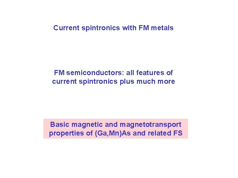
Current spintronics with FM metals FM semiconductors: all features of current spintronics plus much more Basic magnetic and magnetotransport properties of (Ga, Mn)As and related FS

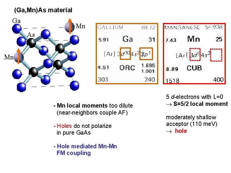
(Ga, Mn)As material Ga Mn As Mn - Mn local moments too dilute (near-neighbors couple AF) - Holes do not polarize in pure Ga. As - Hole mediated Mn-Mn FM coupling 5 d-electrons with L=0 S=5/2 local moment moderately shallow acceptor (110 me. V) hole

Ferromagnetic semiconductor Ga. As: Mn DOS spin Exchange-split, SOcoupled, & itinerant holes EF << 1% Mn ~1% Mn >2% Mn Energy spin onset of ferromagnetism near MIT As-p-like holes localized on Mn acceptors valence band As-p-like holes Ga Mn Mn-d-like local moments Mn As

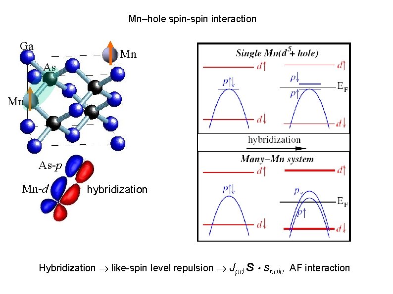
Mn–hole spin-spin interaction Ga Mn As-p Mn-d hybridization Hybridization like-spin level repulsion Jpd S shole AF interaction

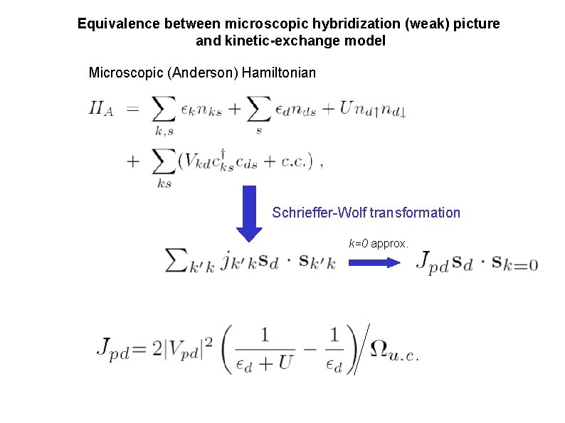
Equivalence between microscopic hybridization (weak) picture and kinetic-exchange model Microscopic (Anderson) Hamiltonian Schrieffer-Wolf transformation k=0 approx.

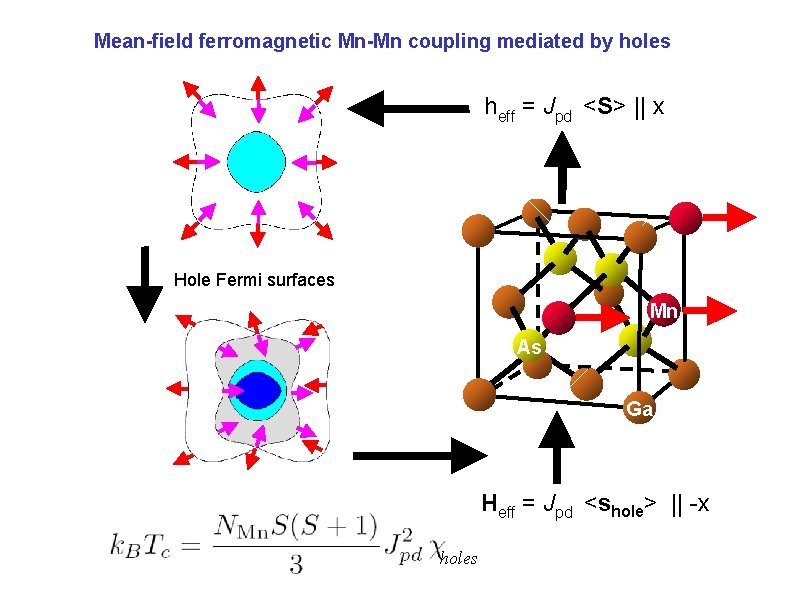
Mean-field ferromagnetic Mn-Mn coupling mediated by holes heff = Jpd <S> || x Hole Fermi surfaces Mn As Ga Heff = Jpd <shole> || -x holes

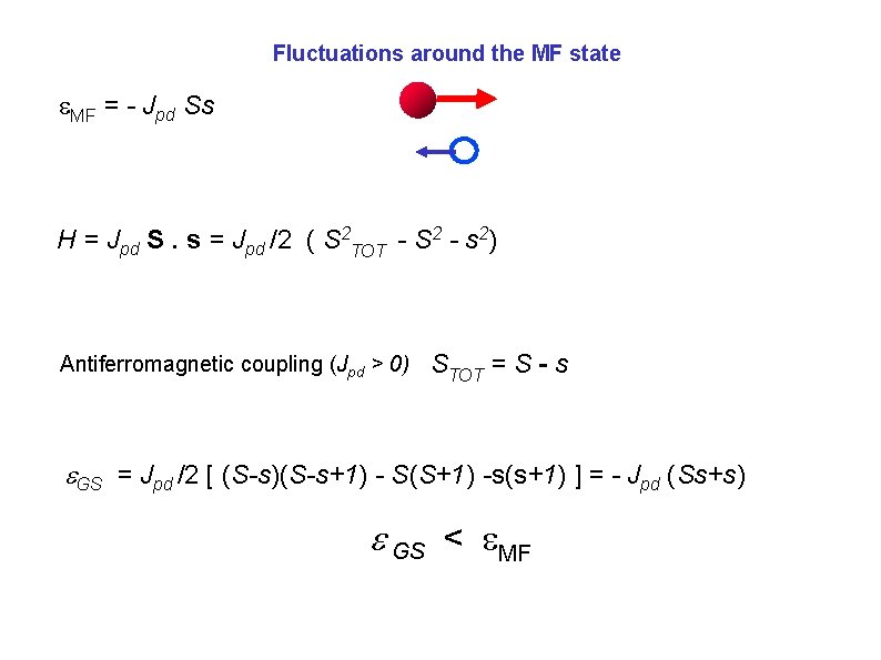
Fluctuations around the MF state e. MF = - Jpd Ss H = Jpd S. s = Jpd /2 ( S 2 TOT - S 2 - s 2) Antiferromagnetic coupling (Jpd > 0) STOT = S - s e. GS = Jpd /2 [ (S-s)(S-s+1) - S(S+1) -s(s+1) ] = - Jpd (Ss+s) e GS < e. MF

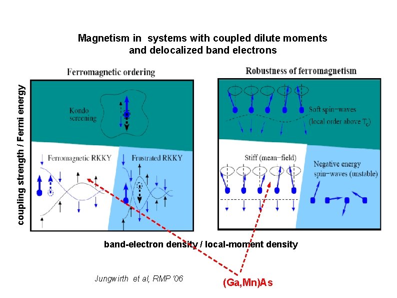
coupling strength / Fermi energy Magnetism in systems with coupled dilute moments and delocalized band electrons band-electron density / local-moment density Jungwirth et al, RMP '06 (Ga, Mn)As

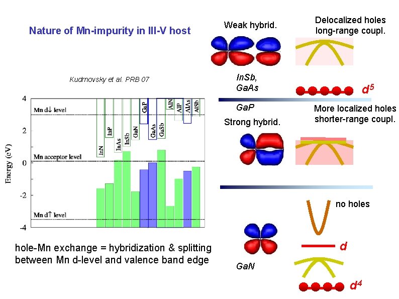
Nature of Mn-impurity in III-V host Kudrnovsky et al. PRB 07 Weak hybrid. Delocalized holes long-range coupl. In. Sb, Ga. As Ga. P Strong hybrid. d 5 More localized holes shorter-range coupl. no holes hole-Mn exchange = hybridization & splitting between Mn d-level and valence band edge d Ga. N d 4

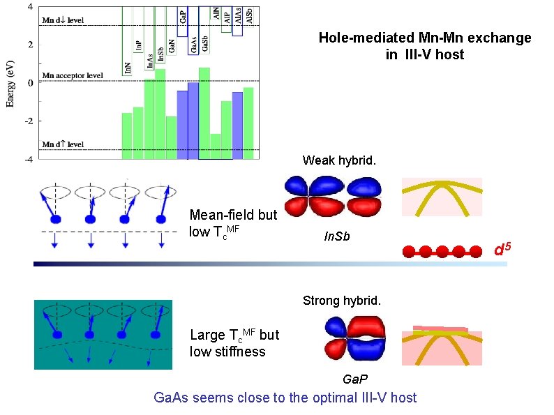
Hole-mediated Mn-Mn exchange in III-V host Weak hybrid. Mean-field but low Tc. MF In. Sb Strong hybrid. Large Tc. MF but low stiffness Ga. P Ga. As seems close to the optimal III-V host d 5

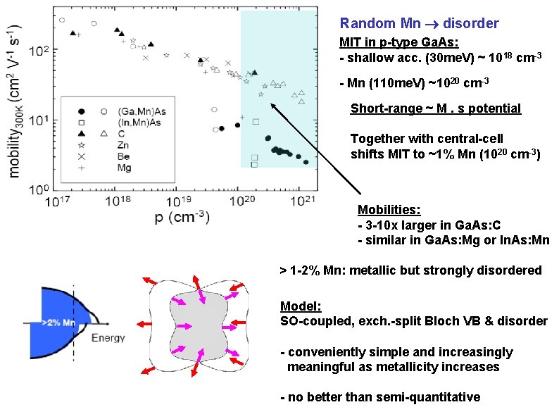
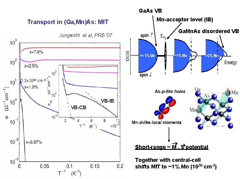
Random Mn disorder MIT in p-type Ga. As: - shallow acc. (30 me. V) ~ 1018 cm-3 - Mn (110 me. V) ~1020 cm-3 Short-range ~ M. s potential Together with central-cell shifts MIT to ~1% Mn (1020 cm-3) Mobilities: - 3 -10 x larger in Ga. As: C - similar in Ga. As: Mg or In. As: Mn > 1 -2% Mn: metallic but strongly disordered Model: SO-coupled, exch. -split Bloch VB & disorder - conveniently simple and increasingly meaningful as metallicity increases - no better than semi-quantitative

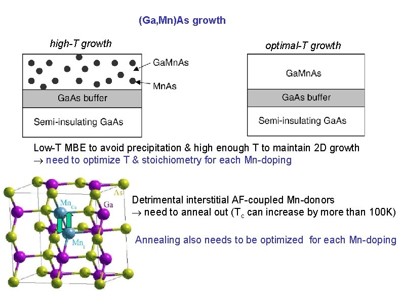
(Ga, Mn)As growth high-T growth optimal-T growth Low-T MBE to avoid precipitation & high enough T to maintain 2 D growth need to optimize T & stoichiometry for each Mn-doping Detrimental interstitial AF-coupled Mn-donors need to anneal out (Tc can increase by more than 100 K) Annealing also needs to be optimized for each Mn-doping

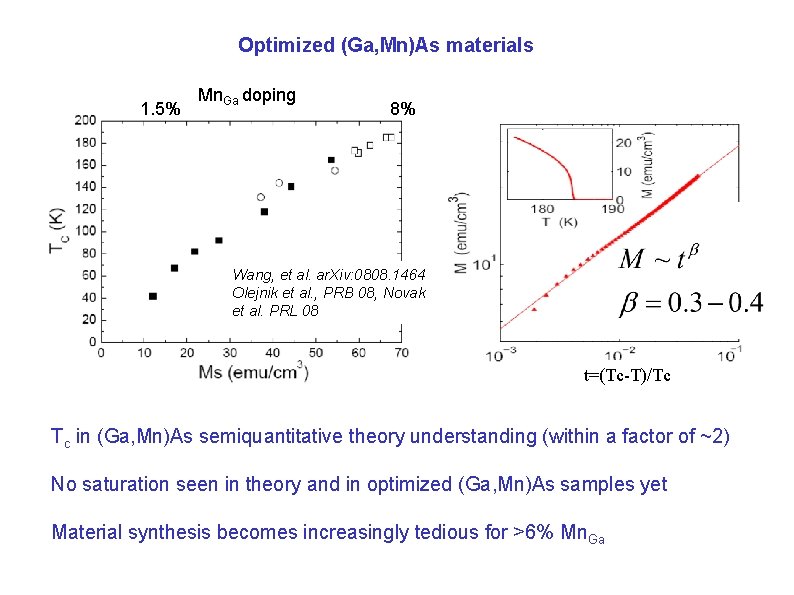
Optimized (Ga, Mn)As materials 1. 5% Mn. Ga doping 8% Wang, et al. ar. Xiv: 0808. 1464 Olejnik et al. , PRB 08, Novak et al. PRL 08 t=(Tc-T)/Tc Tc in (Ga, Mn)As semiquantitative theory understanding (within a factor of ~2) No saturation seen in theory and in optimized (Ga, Mn)As samples yet Material synthesis becomes increasingly tedious for >6% Mn. Ga

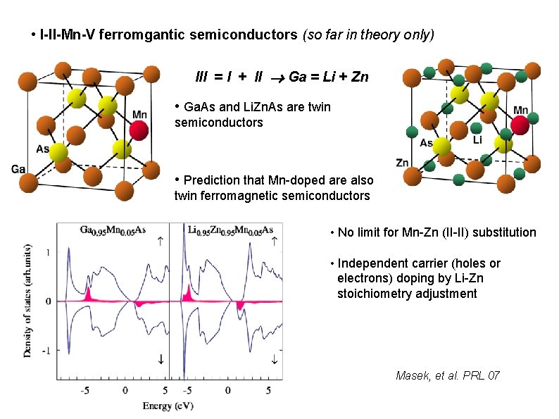
• I-II-Mn-V ferromgantic semiconductors (so far in theory only) III = I + II Ga = Li + Zn • Ga. As and Li. Zn. As are twin semiconductors • Prediction that Mn-doped are also twin ferromagnetic semiconductors • No limit for Mn-Zn (II-II) substitution • Independent carrier (holes or electrons) doping by Li-Zn stoichiometry adjustment Masek, et al. PRL 07

Ga. As VB Transport in (Ga, Mn)As: MIT Jungwirth et al, PRB '07 Mn-acceptor level (IB) Ga. Mn. As disordered VB 2. 2 x 1020 cm-3 VB-IB VB-CB Short-range ~ M. s potential Together with central-cell shifts MIT to ~1% Mn (1020 cm-3)

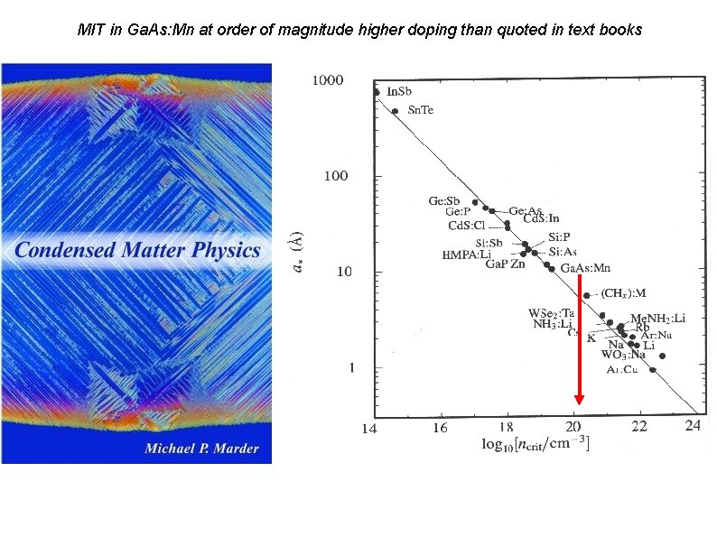
MIT in Ga. As: Mn at order of magnitude higher doping than quoted in text books

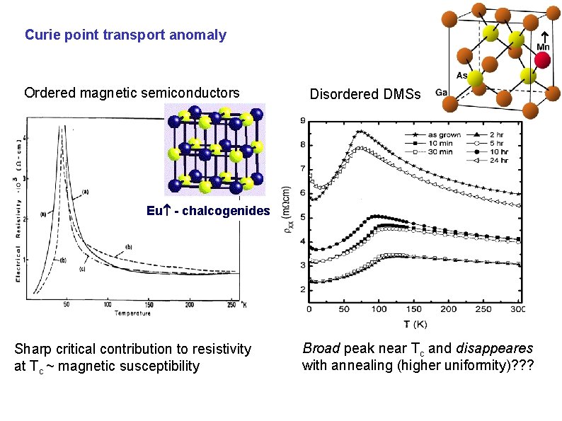
Curie point transport anomaly Ordered magnetic semiconductors Disordered DMSs Eu - chalcogenides Sharp critical contribution to resistivity at Tc ~ magnetic susceptibility Broad peak near Tc and disappeares with annealing (higher uniformity)? ? ?

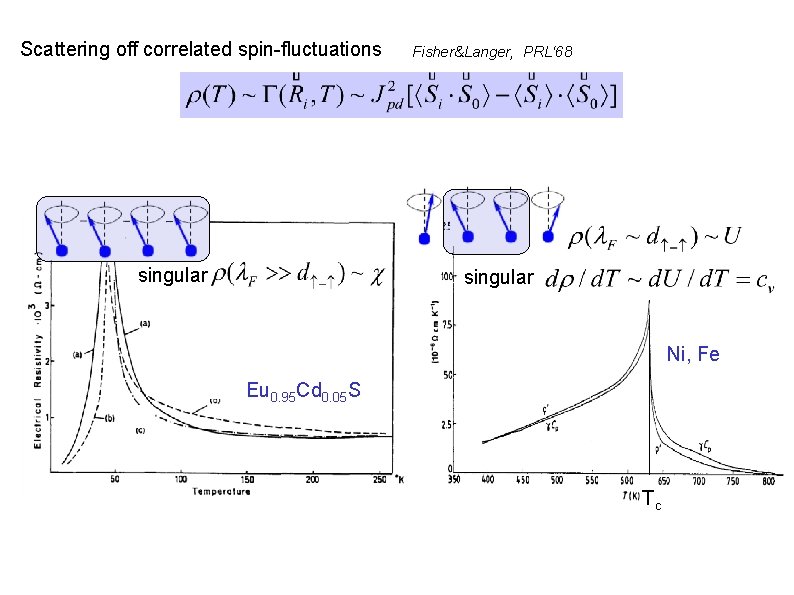
Scattering off correlated spin-fluctuations singular Fisher&Langer, PRL‘ 68 singular Ni, Fe Eu 0. 95 Cd 0. 05 S Tc

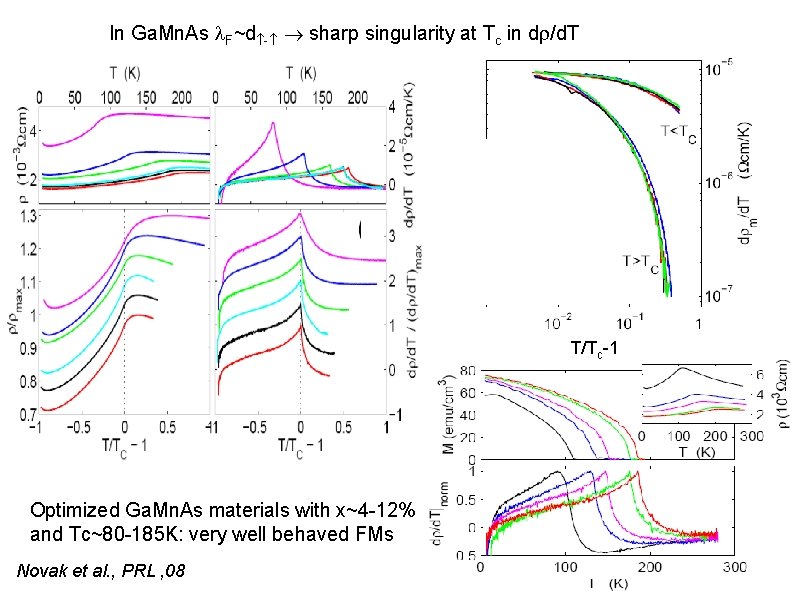
In Ga. Mn. As F~d - sharp singularity at Tc in d /d. T Annealing sequence T/Tc-1 Optimized Ga. Mn. As materials with x~4 -12% and Tc~80 -185 K: very well behaved FMs Novak et al. , PRL ‚ 08

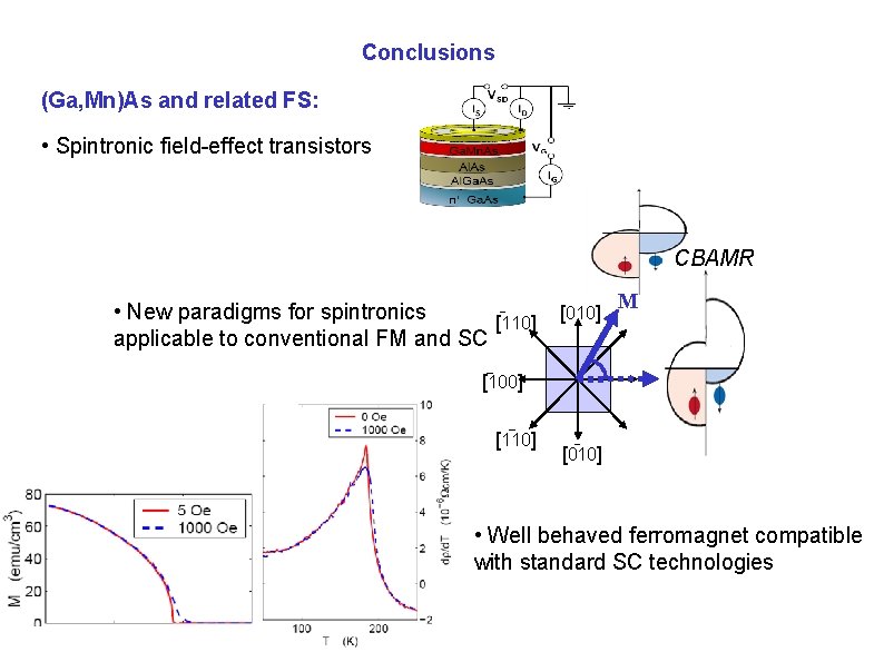
Conclusions (Ga, Mn)As and related FS: • Spintronic field-effect transistors CBAMR • New paradigms for spintronics [110] applicable to conventional FM and SC [010] M [100] [110] [010] • Well behaved ferromagnet compatible with standard SC technologies