Ferroelectric FETs Reference Rainer waser Introduction Replacing of


 states. 2. Chemical")


- Slides: 9
Ferroelectric FETs Reference - Rainer waser
Introduction • Replacing of the gate dielectric of a MOSFET by a ferroelectric material. • If the ferroelectric polarization PFE is normal to the gate plane, it contributes to the charge balance which controls the channel of the FET. • Switching PFE between the two states results in a corresponding shift of the channel threshold voltage of the FET. • This introduces additional functionality into FETs, which is similar to the floating gate in a floating gate transistor used in Flash memories.
Advantages • A typical application area of Fe. FET are nonvolatile memories because they combine some advantages of Fe. RAM and Flash memories. • Fe. RAM – Fe. FETs are 1 -transistor(1 T) memories which avoid large (folded) capacitors required in Fe. RAM, and they offer non-destructive readout(i. e. Memory state is not destroyed during reading).
Advantages & Applications • Flash memories – Fe. FETs show inherently a much faster switching and a significantly lower switching voltage. • Low data retention is drawback of Fe. FET. • Applications (Low retention time are no issues) – Buffer memories at the periphery of large mass storage devices (Flash based solid-state discs)
Challenges in Realization of Fe. FETs 1. High density of interface(trap) states. 2. Chemical reactions and intermixing at the Si/Ferroelectrics interface because of the missing thermodynamic stability. 3. Lattice mismatch between Si and the ferroelectrics(typically perovskite-type) 4. A suitable band offset 2 & 3 can be minimized but not 1 & 4 (this can be overcome by using alternating gate stacks and various buffer layer configurations)
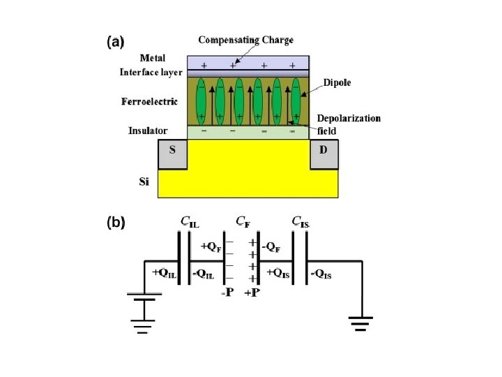
Gate stacks of Fe. FET 1. Metal/Ferroelectric/Si MFS semiconductor- Poor electrical characteristics Severe charge injection into the ferroelectrics Very poor retention 2. Metal/Ferroelectric/buffer semiconductor-MFIS Insulator/Si very thin insulator such as Si. O 2 or high-k oxide is introduced to avoid the above mentioned issues.
3. MFMIS-Gate electrode metal/ ferroelectric/metal/buffer insulator/Si semiconductor 4. MFOXS-Gate electrode metal/ferroelectric/oxide semiconductor
Metal/Ferroelectric/buffer Insulator/Si semiconductor-MFIS • The buffer layer weakens the external electric field across the ferroelectric. • To minimize reduction, the buffer layer thickness should be as small as possible and its permittivity should be as large as possible.