FEI 4 pixel readout chip and IBL module
FE-I 4 pixel readout chip and IBL module Marlon Barbero Bonn University On behalf of ATLAS FE-I 4 / IBL collaboration Vertex 2011 Workshop, Rust - Austria, June 19 th - 24 th 2011
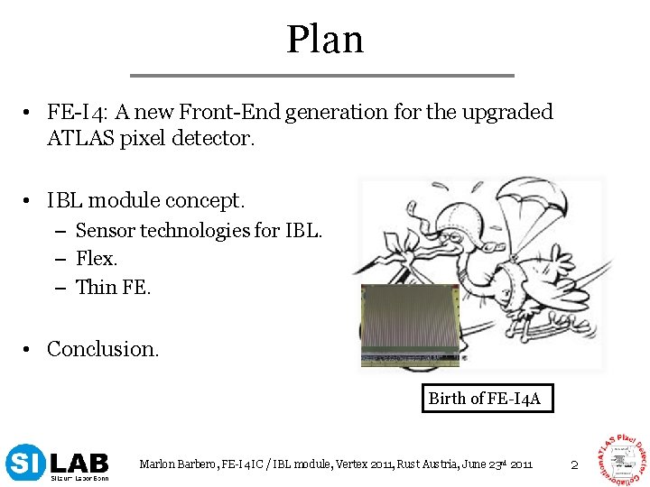
Plan • FE-I 4: A new Front-End generation for the upgraded ATLAS pixel detector. • IBL module concept. – Sensor technologies for IBL. – Flex. – Thin FE. • Conclusion. Birth of FE-I 4 A Marlon Barbero, FE-I 4 IC / IBL module, Vertex 2011, Rust Austria, June 23 rd 2011 2
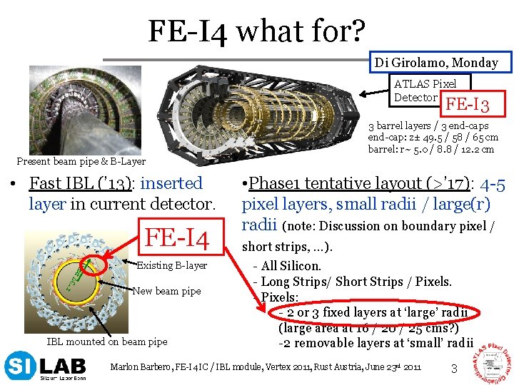
FE-I 4 what for? Di Girolamo, Monday ATLAS Pixel Detector FE-I 3 3 barrel layers / 3 end-caps end-cap: z± 49. 5 / 58 / 65 cm barrel: r~ 5. 0 / 8. 8 / 12. 2 cm Present beam pipe & B-Layer • Fast IBL (’ 13): inserted layer in current detector. Existing B-layer r~ 37 mm FE-I 4 New beam pipe IBL mounted on beam pipe • Phase 1 tentative layout (>’ 17): 4 -5 pixel layers, small radii / large(r) radii (note: Discussion on boundary pixel / short strips, …). - All Silicon. - Long Strips/ Short Strips / Pixels. - Pixels: - 2 or 3 fixed layers at ‘large’ radii (large area at 16 / 20 / 25 cms? ) -2 removable layers at ‘small’ radii Marlon Barbero, FE-I 4 IC / IBL module, Vertex 2011, Rust Austria, June 23 rd 2011 3
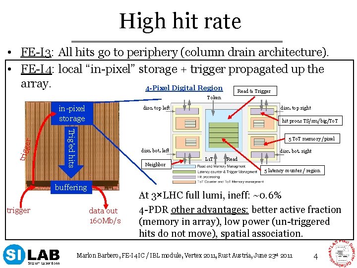
High hit rate storage buffering trigger data out 160 Mb/s 100 Token 3 LHC 60 disc. top right s. LHC disc. top left 80 hit proc. : TS/sm/big/To. T 5 To. T memory /pixel FE-I 3 at r=3. 7 cm! 40 disc. bot. left disc. bot. right LHC er trigg All hits Trig’ed hits in-pixel storage Inefficiency [%] • FE-I 3: All hits go to periphery (column drain architecture). • FE-I 4: local “in-pixel” storage + trigger propagated up the array. 4 -Pixel Digital Region Read & Trigger Neighbor 20 0 0 0. 5 L 1 T Read 5 latency counter / region 1 1. 5 2 2. 5 3 3. 5 4 4. 5 5 At 3×LHC full lumi, ineff: ~0. 6% Hit prob. / DC “inefficiency wall” 4 -PDR other The advantages: better active fraction (memory in array), low power (un-triggered hits do not move), spatial association. Marlon Barbero, FE-I 4 IC / IBL module, Vertex 2011, Rust Austria, June 23 rd 2011 4
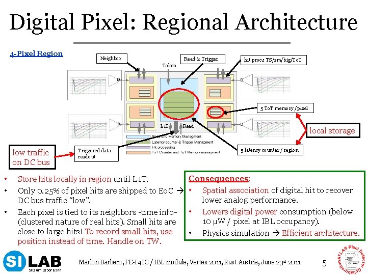
Digital Pixel: Regional Architecture 4 -Pixel Region Neighbor Read & Trigger Token hit proc. : TS/sm/big/To. T 5 To. T memory /pixel L 1 T low traffic on DC bus • • • Read Triggered data readout Store hits locally in region until L 1 T. Only 0. 25% of pixel hits are shipped to Eo. C DC bus traffic “low”. Each pixel is tied to its neighbors -time info(clustered nature of real hits). Small hits are close to large hits! To record small hits, use position instead of time. Handle on TW. local storage 5 latency counter / region Consequences: • Spatial association of digital hit to recover lower analog performance. • Lowers digital power consumption (below 10 μW / pixel at IBL occupancy). • Physics simulation Efficient architecture. Marlon Barbero, FE-I 4 IC / IBL module, Vertex 2011, Rust Austria, June 23 rd 2011 5

Process & granularity • FE-I 3: 0. 25µm process, 50× 400µm 2. • FE-I 4: 130 nm process, 50× 250µm 2. FE-I 3, 250 nm 50 mm 50 μm 250 mm synthezised digital region (1/4 th ) 400 μm • Radiation hardness with minimal effort & substrate isolation (T 3 well) Can use standard synthesized cells! Needed ELT for radiation-tolerance. • • Tolerant to to 250 MRad • 8 -metal layers, good power distribution Can make big IC. Marlon Barbero, FE-I 4 IC / IBL module, Vertex 2011, Rust Austria, June 23 rd 2011 6
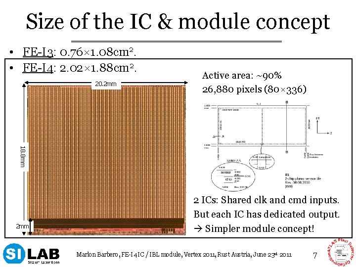
Size of the IC & module concept • FE-I 3: 0. 76× 1. 08 cm 2. • FE-I 4: 2. 02× 1. 88 cm Active area: 74%. 2. 20. 2 mm • 2, 880 pixel (18× 160). Active area: ~90% 26, 880 pixels (80× 336) 7. 6 mm 18. 8 mm 10. 8 mm 2. 8 mm Pixel array Periphery • 2 mm 16 -FE-I 3 module with MCC 2 ICs: Shared clk and cmd inputs. But each IC has dedicated output. Simpler module concept! Marlon Barbero, FE-I 4 IC / IBL module, Vertex 2011, Rust Austria, June 23 rd 2011 7
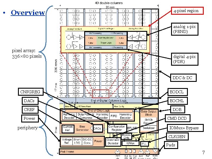
4 -pixel region • Overview analog 1 -pix (FEND) pixel array: 336× 80 pixels digital 4 -pix (PDR) DDC & DC CNFGREG EODCL DACs EOCHL CREF DOB Power CMD DCD periphery IOMux+ Bypass CLKGEN Pads Marlon Barbero, FE-I 4 IC / IBL module, Vertex 2011, Rust Austria, June 23 rd 2011 8 7
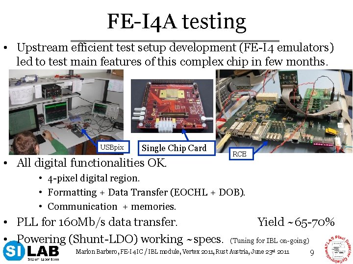
FE-I 4 A testing • Upstream efficient test setup development (FE-I 4 emulators) led to test main features of this complex chip in few months. USBpix Single Chip Card • All digital functionalities OK. RCE • 4 -pixel digital region. • Formatting + Data Transfer (EOCHL + DOB). • Communication + memories. • PLL for 160 Mb/s data transfer. • Powering (Shunt-LDO) working ~specs. Yield ~65 -70% (Tuning for IBL on-going) Marlon Barbero, FE-I 4 IC / IBL module, Vertex 2011, Rust Austria, June 23 rd 2011 9
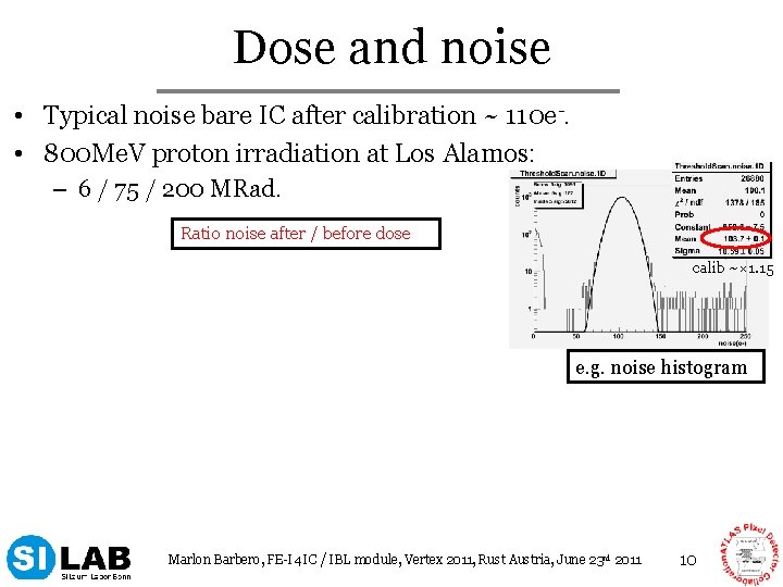
Dose and noise • Typical noise bare IC after calibration ~ 110 e-. • 800 Me. V proton irradiation at Los Alamos: – 6 / 75 / 200 MRad. Ratio noise after / before dose calib ~× 1. 15 e. g. noise histogram Marlon Barbero, FE-I 4 IC / IBL module, Vertex 2011, Rust Austria, June 23 rd 2011 10
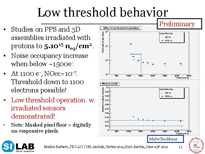
Low threshold behavior • Studies on PPS and 3 D assemblies irradiated with protons to 5. 1015 neq/cm 2. • Noise occupancy increase when below ~1500 e-. • At 1100 e-, NOcc~10 -7. Threshold down to 1100 electrons possible! • Low threshold operation w. irradiated sensors demonstrated! • Preliminary Note: Masked pixel floor = digitally un-responsive pixels. Malte Backhaus Marlon Barbero, FE-I 4 IC / IBL module, Vertex 2011, Rust Austria, June 23 rd 2011 11

IBL Sensor Specifications • IBL environment: Radiation hard FE and sensor. • For now, two different pixel sensor technology candidates: n-in -n planar / partial-3 D silicon. • Specifications: – – – HV: max 1000 V. Thickness: 225± 25µm. Max. power dissipation: 200 m. W/cm 2 at -15 o. C. No shingling in z Edge width: below 450µm. Tracking efficiency: above 98%. • Choice for technology: Install Summer 2013 Sensor Prod. completed Summer 2012 Sensor choice in July 2011. Detailed schedule / Procurement: Pernegger Tuesday Marlon Barbero, FE-I 4 IC / IBL module, Vertex 2011, Rust Austria, June 23 rd 2011 12
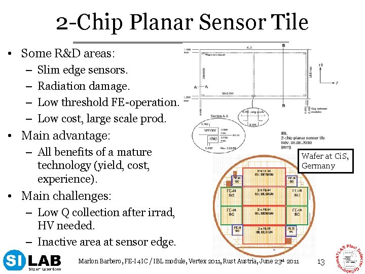
2 -Chip Planar Sensor Tile • Some R&D areas: – – Slim edge sensors. Radiation damage. Low threshold FE-operation. Low cost, large scale prod. • Main advantage: – All benefits of a mature technology (yield, cost, experience). Wafer at Ci. S, Germany • Main challenges: – Low Q collection after irrad, HV needed. – Inactive area at sensor edge. Marlon Barbero, FE-I 4 IC / IBL module, Vertex 2011, Rust Austria, June 23 rd 2011 13
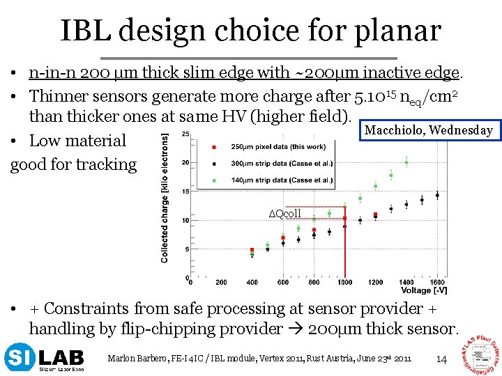
IBL design choice for planar • n-in-n 200 µm thick slim edge with ~200µm inactive edge. • Thinner sensors generate more charge after 5. 1015 neq/cm 2 than thicker ones at same HV (higher field). Macchiolo, Wednesday • Low material good for tracking ΔQcoll • + Constraints from safe processing at sensor provider + handling by flip-chipping provider 200µm thick sensor. Marlon Barbero, FE-I 4 IC / IBL module, Vertex 2011, Rust Austria, June 23 rd 2011 14
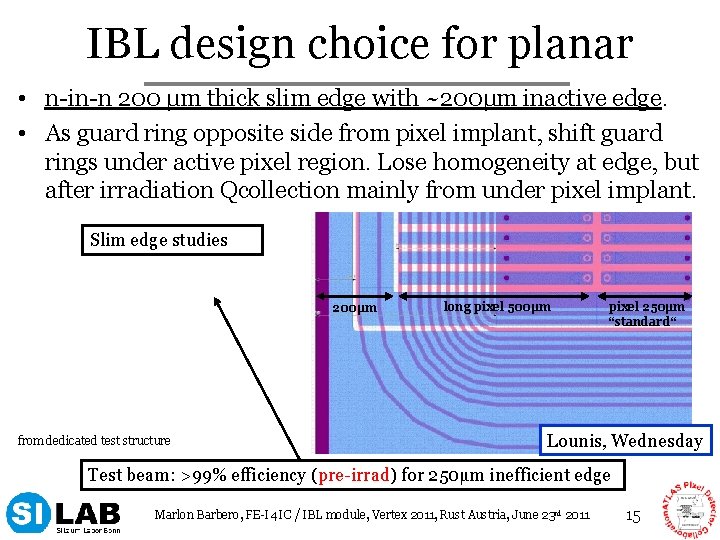
IBL design choice for planar • n-in-n 200 µm thick slim edge with ~200µm inactive edge. • As guard ring opposite side from pixel implant, shift guard rings under active pixel region. Lose homogeneity at edge, but after irradiation Qcollection mainly from under pixel implant. Slim edge studies 200µm from dedicated test structure long pixel 500µm pixel 250µm “standard“ Lounis, Wednesday Test beam: >99% efficiency (pre-irrad) for 250µm inefficient edge Marlon Barbero, FE-I 4 IC / IBL module, Vertex 2011, Rust Austria, June 23 rd 2011 15
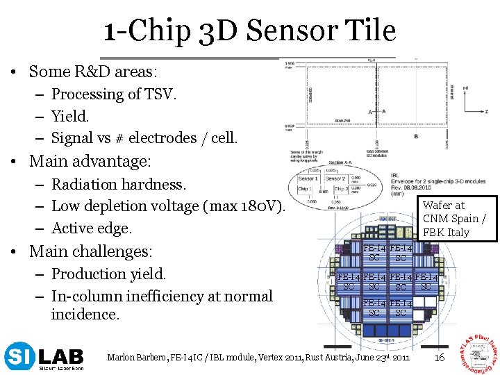
1 -Chip 3 D Sensor Tile • Some R&D areas: – Processing of TSV. – Yield. – Signal vs # electrodes / cell. • Main advantage: – Radiation hardness. – Low depletion voltage (max 180 V). – Active edge. • Main challenges: – Production yield. – In-column inefficiency at normal incidence. Wafer at CNM Spain / FBK Italy FE-I 4 SC SC FE-I 4 SC SC Marlon Barbero, FE-I 4 IC / IBL module, Vertex 2011, Rust Austria, June 23 rd 2011 16
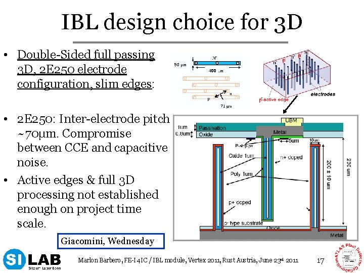
IBL design choice for 3 D • Double-Sided full passing 3 D, 2 E 250 electrode configuration, slim edges: • 2 E 250: Inter-electrode pitch ~70µm. Compromise between CCE and capacitive noise. • Active edges & full 3 D processing not established enough on project time scale. Giacomini, Wednesday Marlon Barbero, FE-I 4 IC / IBL module, Vertex 2011, Rust Austria, June 23 rd 2011 17
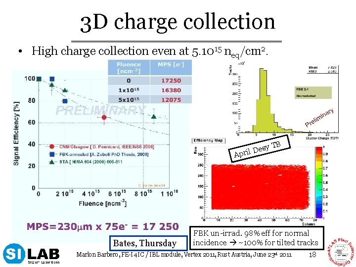
3 D charge collection • High charge collection even at 5. 1015 neq/cm 2. y TB Des April Bates, Thursday FBK un-irrad. 98% eff for normal incidence ~100% for tilted tracks Marlon Barbero, FE-I 4 IC / IBL module, Vertex 2011, Rust Austria, June 23 rd 2011 18
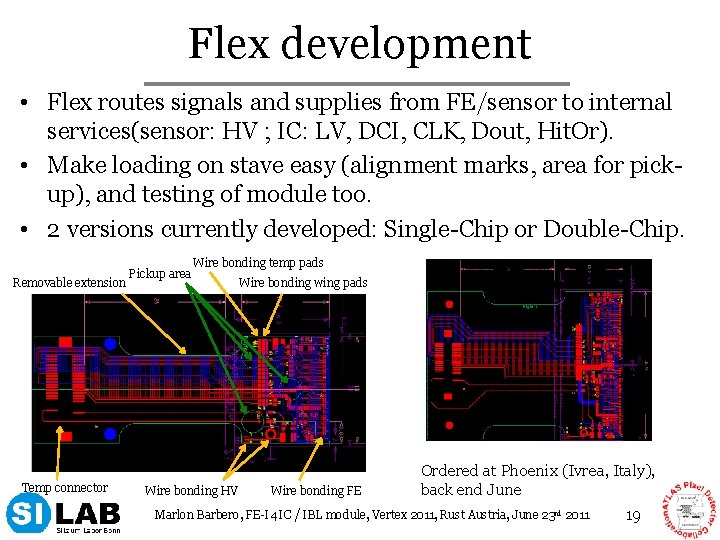
Flex development • Flex routes signals and supplies from FE/sensor to internal services(sensor: HV ; IC: LV, DCI, CLK, Dout, Hit. Or). • Make loading on stave easy (alignment marks, area for pickup), and testing of module too. • 2 versions currently developed: Single-Chip or Double-Chip. Removable extension Temp connector Pickup area Wire bonding temp pads Wire bonding HV Wire bonding wing pads Wire bonding FE Ordered at Phoenix (Ivrea, Italy), back end June Marlon Barbero, FE-I 4 IC / IBL module, Vertex 2011, Rust Austria, June 23 rd 2011 19
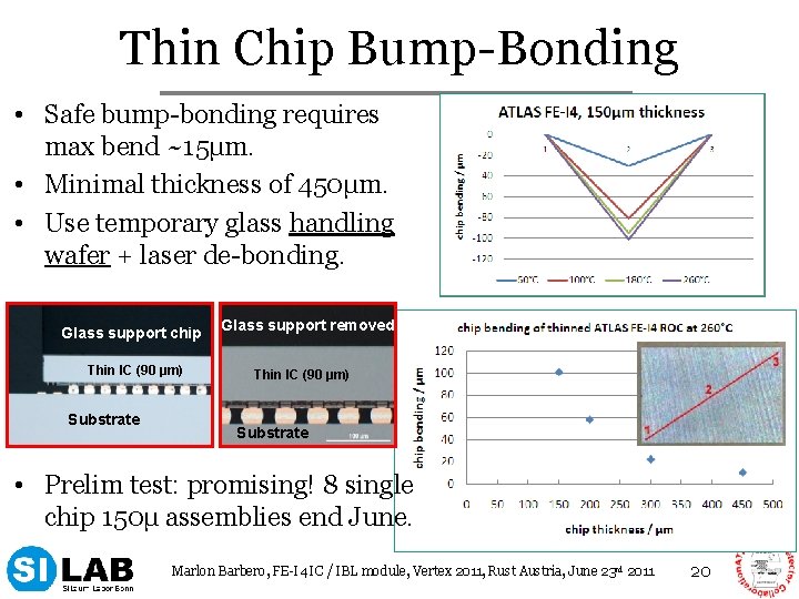
Thin Chip Bump-Bonding • Safe bump-bonding requires max bend ~15µm. • Minimal thickness of 450µm. • Use temporary glass handling wafer + laser de-bonding. Glass support chip Thin IC (90 µm) Substrate Glass support removed Thin IC (90 µm) Substrate • Prelim test: promising! 8 single chip 150µ assemblies end June. Marlon Barbero, FE-I 4 IC / IBL module, Vertex 2011, Rust Austria, June 23 rd 2011 20
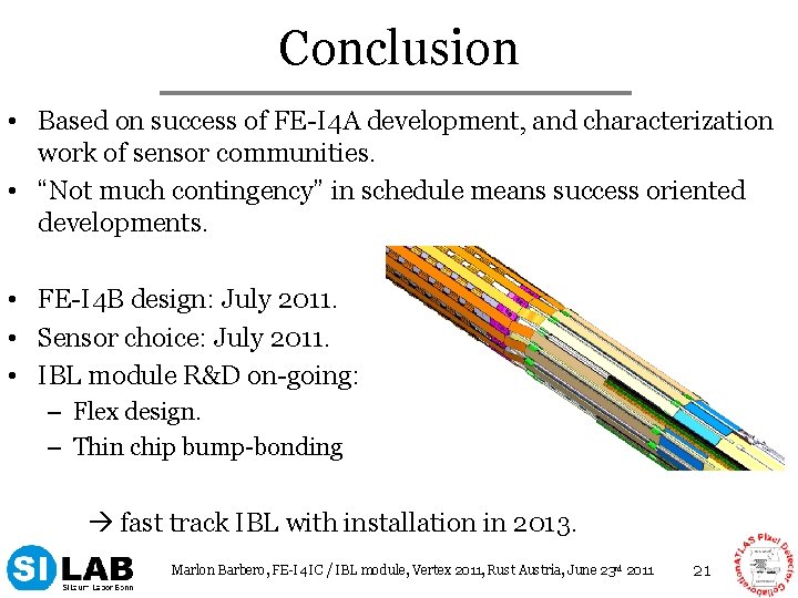
Conclusion • Based on success of FE-I 4 A development, and characterization work of sensor communities. • “Not much contingency” in schedule means success oriented developments. • FE-I 4 B design: July 2011. • Sensor choice: July 2011. • IBL module R&D on-going: – Flex design. – Thin chip bump-bonding fast track IBL with installation in 2013. Marlon Barbero, FE-I 4 IC / IBL module, Vertex 2011, Rust Austria, June 23 rd 2011 21
Backup BACKUP Marlon Barbero, FE-I 4 IC / IBL module, Vertex 2011, Rust Austria, June 23 rd 2011 22
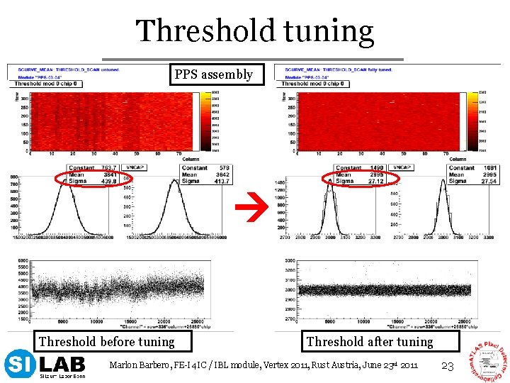
Threshold tuning PPS assembly Threshold before tuning Threshold after tuning Marlon Barbero, FE-I 4 IC / IBL module, Vertex 2011, Rust Austria, June 23 rd 2011 23
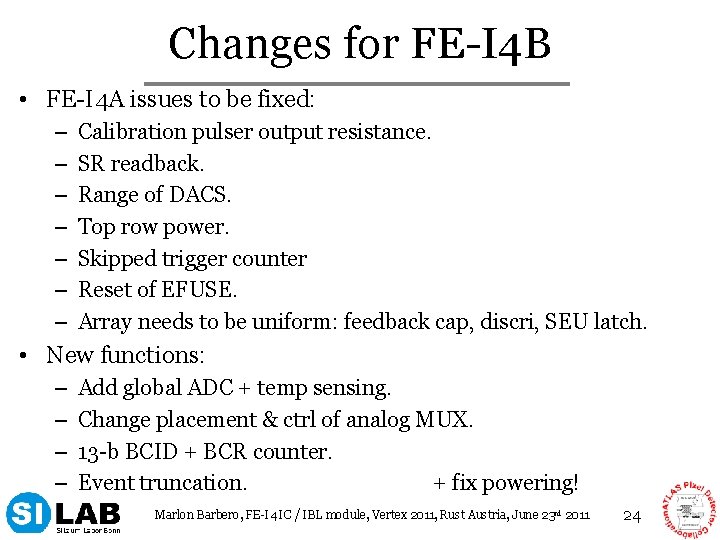
Changes for FE-I 4 B • FE-I 4 A issues to be fixed: – – – – Calibration pulser output resistance. SR readback. Range of DACS. Top row power. Skipped trigger counter Reset of EFUSE. Array needs to be uniform: feedback cap, discri, SEU latch. • New functions: – – Add global ADC + temp sensing. Change placement & ctrl of analog MUX. 13 -b BCID + BCR counter. Event truncation. + fix powering! Marlon Barbero, FE-I 4 IC / IBL module, Vertex 2011, Rust Austria, June 23 rd 2011 24
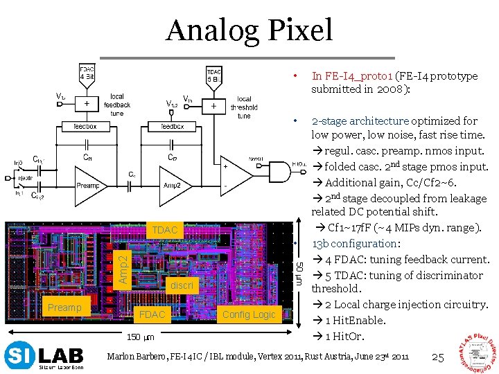
Analog Pixel • In FE-I 4_proto 1 (FE-I 4 prototype submitted in 2008): • 2 -stage architecture optimized for low power, low noise, fast rise time. regul. casc. preamp. nmos input. folded casc. 2 nd stage pmos input. Additional gain, Cc/Cf 2~6. 2 nd stage decoupled from leakage related DC potential shift. Cf 1~17 f. F (~4 MIPs dyn. range). 13 b configuration: 4 FDAC: tuning feedback current. 5 TDAC: tuning of discriminator threshold. 2 Local charge injection circuitry. 1 Hit. Enable. 1 Hit. Or. TDAC Preamp 50 mm Amp 2 • discri FDAC 150 mm Config Logic Marlon Barbero, FE-I 4 IC / IBL module, Vertex 2011, Rust Austria, June 23 rd 2011 25
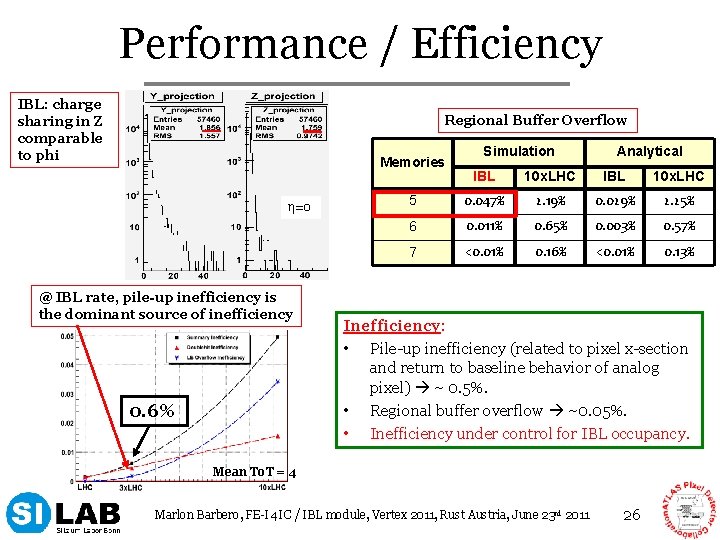
Performance / Efficiency IBL: charge sharing in Z comparable to phi Regional Buffer Overflow Memories η=0 @ IBL rate, pile-up inefficiency is the dominant source of inefficiency 0. 6% Simulation Analytical IBL 10 x. LHC 5 0. 047% 2. 19% 0. 029% 2. 25% 6 0. 011% 0. 65% 0. 003% 0. 57% 7 <0. 01% 0. 16% <0. 01% 0. 13% Inefficiency: • Pile-up inefficiency (related to pixel x-section and return to baseline behavior of analog pixel) ~ 0. 5%. • Regional buffer overflow ~0. 05%. • Inefficiency under control for IBL occupancy. Mean To. T = 4 Marlon Barbero, FE-I 4 IC / IBL module, Vertex 2011, Rust Austria, June 23 rd 2011 26
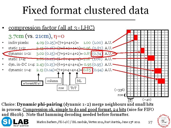
Fixed format clustered data • compression factor (all at 3×LHC) 3. 7 cm (vs. 21 cm), η=0 • • • indiv pixels: static 1× 2: dynamic 1× 2: static 1× 4: dyn. in-DC 1× 4: dynamic 1× 4: 4. 09 (0. 25)×(7+9+4+2)= 1. 00 (1. 00) 3. 45 (0. 18)×(7+8+2× 4+2)=0. 96 (0. 83) 3. 02 (0. 15)×(7+9+2× 4+2)= 0. 87 (0. 74) 2. 86 (0. 17)×(6+8+4× 4+4)=1. 08 (1. 08) 2. 43 (0. 15)×(6+9+4× 4+4)= 0. 95 (0. 95) 2. 13 (0. 14)×(7+9+4× 4+4)= 0. 85 (0. 94) 106. count. FE-1. s-1 column A. U. NL row To. T (× 336) row DC (× 40) Choice: Dynamic phi-pairing (dynamic 1× 2) merge neighbours and small hits in process. Compression ok, simple to do and good format, 24 bits (nice for FIFO and 8 b 10 b). Note that hamming decoding needed before formatter. Marlon Barbero, FE-I 4 IC / IBL module, Vertex 2011, Rust Austria, June 23 rd 2011 27
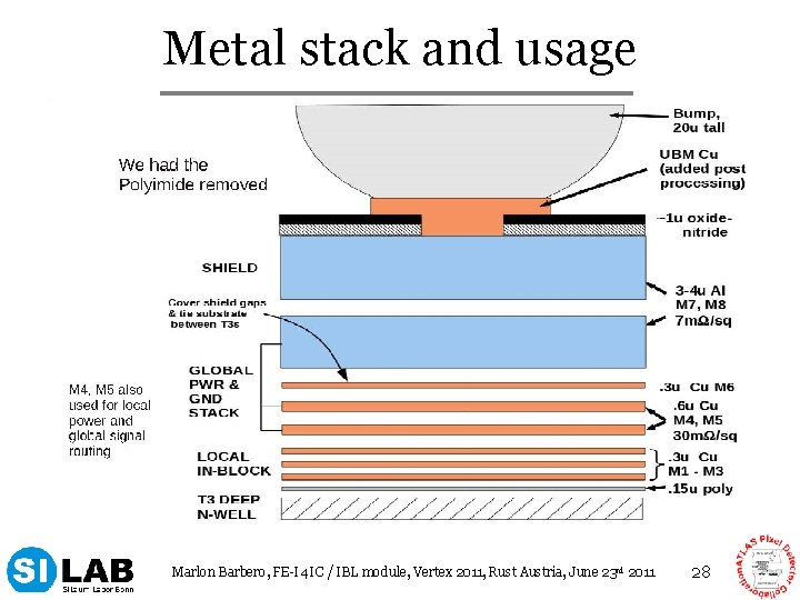
Metal stack and usage Marlon Barbero, FE-I 4 IC / IBL module, Vertex 2011, Rust Austria, June 23 rd 2011 28

Marlon Barbero, FE-I 4 IC / IBL module, Vertex 2011, Rust Austria, June 23 rd 2011 29
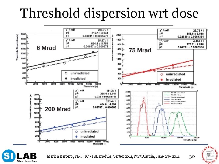
Threshold dispersion wrt dose Marlon Barbero, FE-I 4 IC / IBL module, Vertex 2011, Rust Austria, June 23 rd 2011 30
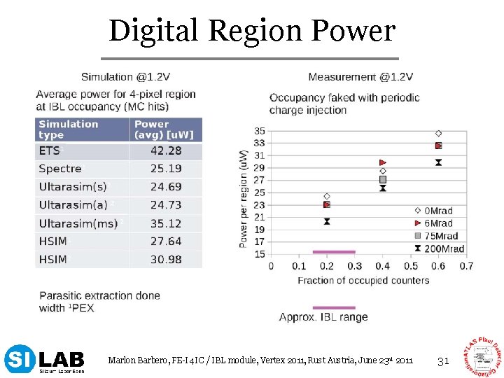
Digital Region Power Marlon Barbero, FE-I 4 IC / IBL module, Vertex 2011, Rust Austria, June 23 rd 2011 31
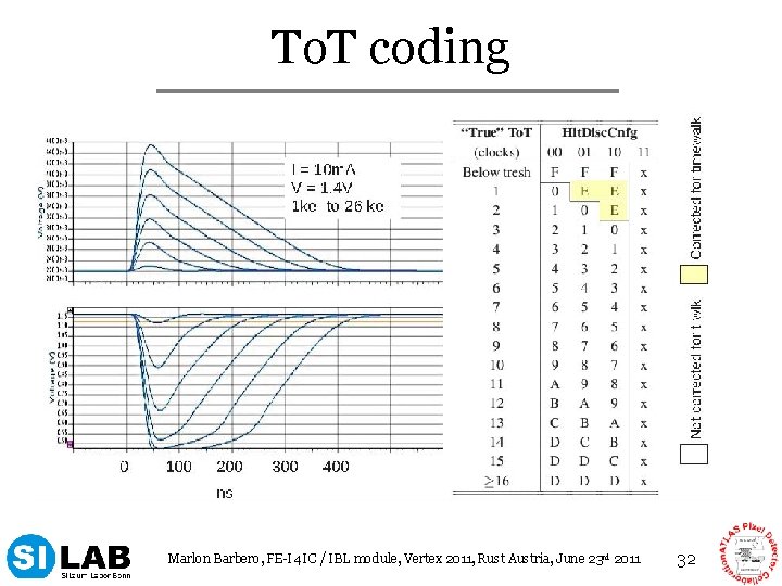
To. T coding Marlon Barbero, FE-I 4 IC / IBL module, Vertex 2011, Rust Austria, June 23 rd 2011 32
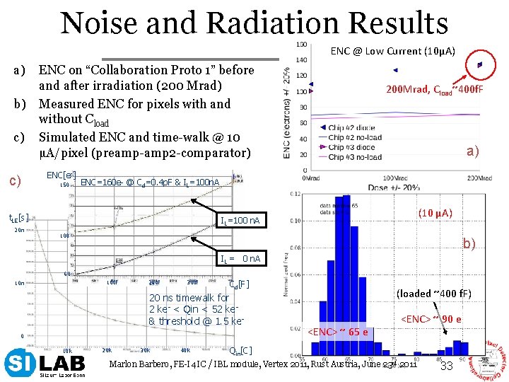
Noise and Radiation Results ENC @ Low Current (10µA) a) b) c) ENC on “Collaboration Proto 1” before and after irradiation (200 Mrad) Measured ENC for pixels with and without Cload Simulated ENC and time-walk @ 10 µA/pixel (preamp-amp 2 -comparator) ENC[e-] c) 150 a) ENC=160 e- @ Cd=0. 4 p. F & IL=100 n. A t. LE[s] 20 n 200 Mrad, Cload~400 f. F (10 µA) IL=100 n. A 100 b) IL = 0 n. A 60 100 f 10 n 200 f 300 f Cd[F] 20 ns timewalk for 2 ke- < Qin < 52 ke& threshold @ 1. 5 ke 0 10 k 20 k 30 k 40 k (loaded ~400 f. F) <ENC> ~ 65 e <ENC> ~ 90 e Qin[C] Marlon Barbero, FE-I 4 IC / IBL module, Vertex 2011, Rust Austria, June 23 rd 2011 33
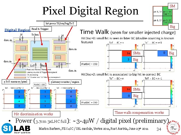
SM Pixel Digital Region hit proc. : TS/sm/big/To. T Digital Region Token N Big Read & Trigger N disc. in Big SMn Big disc. in N L 1 T Read N disc. in 5 To. T memory /pixel 5 latency counter / region SMn Big Hit discrimination works Time walk compensation works • Power (3. 7 cm 3 x. LHC full): ~3 -4µW / digital pixel (preliminary). Marlon Barbero, FE-I 4 IC / IBL module, Vertex 2011, Rust Austria, June 23 rd 2011 34
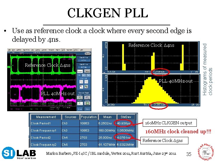
CLKGEN PLL Reference Clock Δ 4 ns PLL 40 MHz out Histograms of measured clock periods • Use as reference clock a clock where every second edge is delayed by 4 ns. 160 MHz CLKGEN output 160 MHz clock cleaned up!!! Reference Clock Δ 5 ns Marlon Barbero, FE-I 4 IC / IBL module, Vertex 2011, Rust Austria, June 23 rd 2011 35

Solder bumping process @ IZM Flip-Chip 36

Thin chip modules – Process flow Support Chip ROC Wafer Dicing of Wafer Stack Wafer Thinning Support Chip Support Wafer Temporary Wafer Bonding to support wafer Bump Bonding Sensor Support Chip Release Support Wafer Contact formation (Micro-Bumping) Marlon Barbero, FE-I 4 IC / IBL module, Vertex 2011, Rust Austria, June 23 rd 2011 37
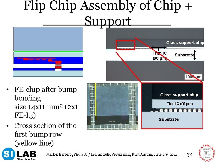
Flip Chip Assembly of Chip + Support Glass support chip Thin IC (90 µm) • FE-chip after bump bonding size 14 x 11 mm² (2 x 1 FE-I 3) • Cross section of the first bump row (yellow line) Substrate Glass support chip Thin IC (90 µm) Substrate Marlon Barbero, FE-I 4 IC / IBL module, Vertex 2011, Rust Austria, June 23 rd 2011 38
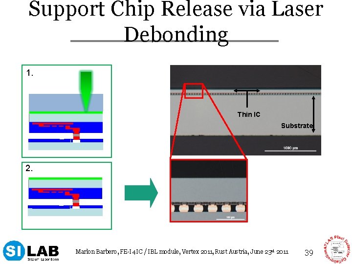
Support Chip Release via Laser Debonding 1. Thin IC Substrate 2. Marlon Barbero, FE-I 4 IC / IBL module, Vertex 2011, Rust Austria, June 23 rd 2011 39

Status thin FE-I 4 modules at IZM • • • 1 FE-I 4 (AUN 6 NGH) wafer have thinned to 470 µm and has been used for 36 assemblies without any bump defects in the corners. Demonstrate the minimum chip thickness of 450 µm. 1 st wafer (AWN 6 TUH) has been thinned to 150 µm, bumped and is currently being used for flip chip assemblies: – Already 5 assemblies (3 D FBK from ATLAS 09) in our hands. – No support chip removal for these assemblies. – 16 more single chip assemblies have been flipped: • 8 bad chips for adjusting laser parameters • 8 good chips – 8 are currently at the laser debonding step in US, 8 more will go to another vendor (in Germany) in the next days. Expected delivery in the next 2 weeks. – Up to 8 2 -chip modules (depending on the number of available FE-I 4 chips) will go to flip chip after the finishing of the 1 st devices 6 more FE-I 4 wafers are currently in bump process: – 4 wafers with thickness of 150 µm – 2 wafers with thickness of 100 µm – UBM and bump deposition finished by mid June. Marlon Barbero, FE-I 4 IC / IBL module, Vertex 2011, Rust Austria, June 23 rd 2011 40
- Slides: 40