FEE Electronics progress PCB layout progress VHDL progress
FEE Electronics progress • PCB layout progress • VHDL progress in TBU • Prototype fixture for software 9 th June 2009
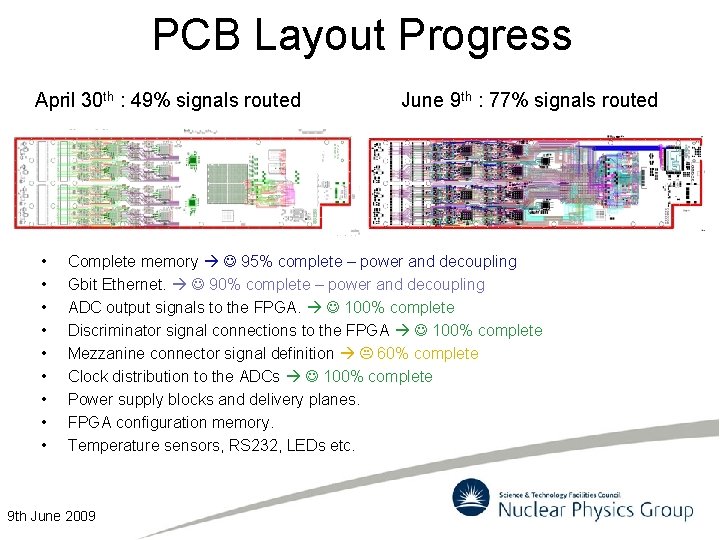
PCB Layout Progress April 30 th : 49% signals routed • • • June 9 th : 77% signals routed Complete memory 95% complete – power and decoupling Gbit Ethernet. 90% complete – power and decoupling ADC output signals to the FPGA. 100% complete Discriminator signal connections to the FPGA 100% complete Mezzanine connector signal definition 60% complete Clock distribution to the ADCs 100% complete Power supply blocks and delivery planes. FPGA configuration memory. Temperature sensors, RS 232, LEDs etc. 9 th June 2009
PCB layout targets • June 30 th : – Complete routing and layout. – Submit to manufacturer for validation and quote. – Submit to assembler for evaluation of assembly and final parts purchase. • July 7 th : – Complete engineering review. • July 14 th : – Submit to pcb manufacturer and assembler. • August 17 th : – Assembled FEE 64 delivered. 9 th June 2009
Collaboration with Detector Systems Development Group of TBU. (Technology Business Unit ) Currently : – Gbit data rate from memory on the devkit => 240 Mbit/sec. – System boots with fallback to golden copy. – Pin allocation of FEE 64 memory and Gbit signals checked. Next steps : – Create a DMA peripheral and check performance. – Create a memory test and configuration system. 9 th June 2009
Prototype fixture for software development Fixture comprises a ZIF socket on a pcb designed to mount a packaged ASIC onto an ML 507 FPGA development board. • Pin out and advice provided by Steve Thomas. • Fixture will allow communications between the ASIC and Linux to be developed. • Mux readout logic VHDL can also be developed. • Design and manufacture of fixture in progress in DL electronic workshops. • Delivery mid June. 9 th June 2009
- Slides: 5