Faculty of Engineering Decimation Filter A Design Perspective
![Faculty of Engineering Digital Filters Background Signal Flow Graphs Operations x 1[n] x[n] y[n]=x Faculty of Engineering Digital Filters Background Signal Flow Graphs Operations x 1[n] x[n] y[n]=x](https://slidetodoc.com/presentation_image_h2/4de2af0e907de6a38ab3ac9d1530def9/image-12.jpg)
![Faculty of Engineering Design of the Comb Filter M X[z] -3 - Y(z) n Faculty of Engineering Design of the Comb Filter M X[z] -3 - Y(z) n](https://slidetodoc.com/presentation_image_h2/4de2af0e907de6a38ab3ac9d1530def9/image-24.jpg)
- Slides: 36

Faculty of Engineering Decimation Filter A Design Perspective Presented by: Sameh Assem Ibrahim 28 -January-2003 Integrated Circuits Laboratory

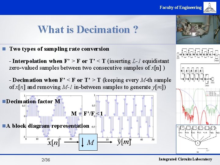
Faculty of Engineering What is Decimation ? n Two types of sampling rate conversion - Interpolation when F’ > F or T’ < T (inserting L-1 equidistant zero-valued samples between two consecutive samples of x[n] ) - Decimation when F’ < F or T’ > T (keeping every M-th sample of x[n] and removing M-1 in-between samples to generate y[m]) n. Decimation factor M M = F’/F <1 n. A block diagram representation x[n] 2/36 M y[m] Integrated Circuits Laboratory

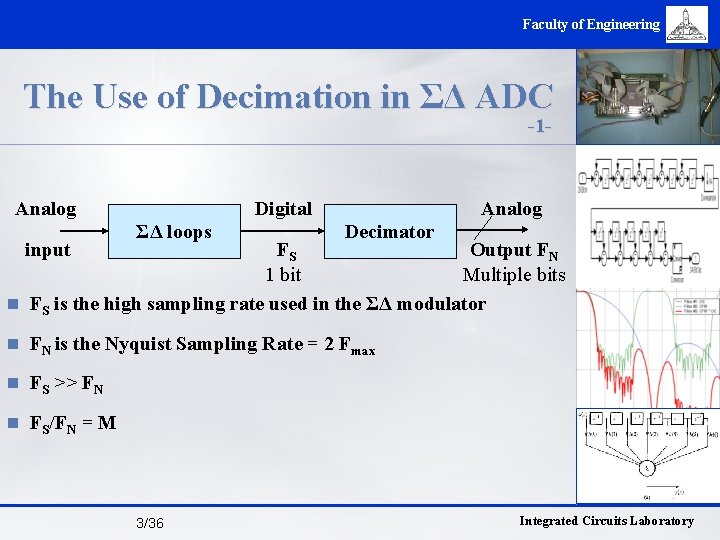
Faculty of Engineering The Use of Decimation in ΣΔ ADC -1 - Analog input Digital ΣΔ loops Analog Decimator FS Output FN 1 bit Multiple bits n FS is the high sampling rate used in the ΣΔ modulator n FN is the Nyquist Sampling Rate = 2 Fmax n FS >> FN n FS/FN = M 3/36 Integrated Circuits Laboratory

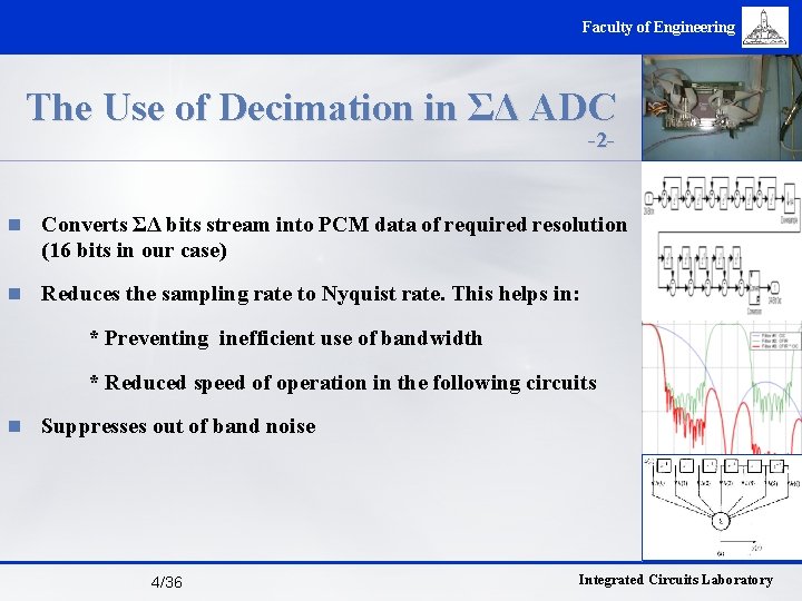
Faculty of Engineering The Use of Decimation in ΣΔ ADC -2 - n Converts ΣΔ bits stream into PCM data of required resolution (16 bits in our case) n Reduces the sampling rate to Nyquist rate. This helps in: * Preventing inefficient use of bandwidth * Reduced speed of operation in the following circuits n Suppresses out of band noise 4/36 Integrated Circuits Laboratory

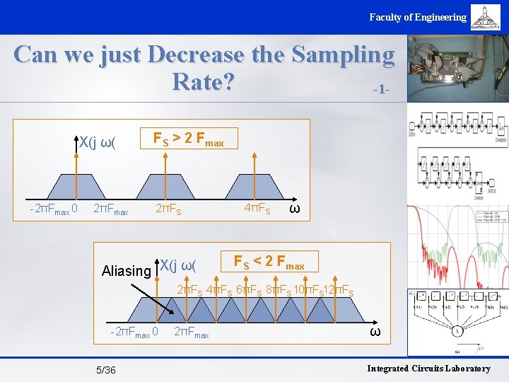
Faculty of Engineering Can we just Decrease the Sampling Rate? -1 X(j ω( -2πFmax 0 2πFmax FS > 2 Fmax 2πFS Aliasing X(j ω( 4πFS ω FS < 2 Fmax 2πFS 4πFS 6πFS 8πFS 10πFS 12πFS -2πFmax 0 5/36 2πFmax ω Integrated Circuits Laboratory

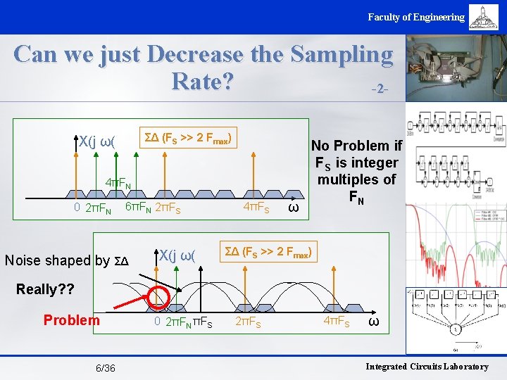
Faculty of Engineering Can we just Decrease the Sampling Rate? -2ΣΔ (FS >> 2 Fmax) X(j ω( 4πFN 0 2πFN 6πFN 2πFS Noise shaped by ΣΔ X(j ω( 4πFS ω No Problem if FS is integer multiples of FN ΣΔ (FS >> 2 Fmax) Really? ? Problem 6/36 0 2πFN πFS 2πFS 4πFS ω Integrated Circuits Laboratory

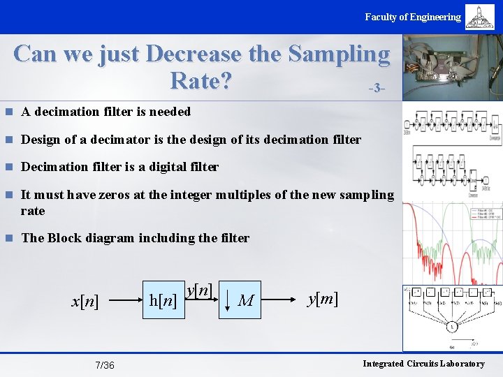
Faculty of Engineering Can we just Decrease the Sampling Rate? -3 n A decimation filter is needed n Design of a decimator is the design of its decimation filter n Decimation filter is a digital filter n It must have zeros at the integer multiples of the new sampling rate n The Block diagram including the filter x[n] 7/36 h[n] y[n] M y[m] Integrated Circuits Laboratory

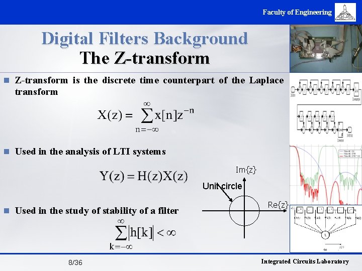
Faculty of Engineering Digital Filters Background The Z-transform n Z-transform is the discrete time counterpart of the Laplace transform n Used in the analysis of LTI systems Im{z} Unit circle n Used in the study of stability of a filter 8/36 Re{z} Integrated Circuits Laboratory

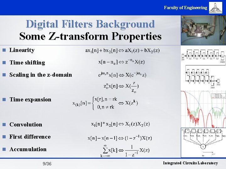
Faculty of Engineering Digital Filters Background Some Z-transform Properties n Linearity n Time shifting n Scaling in the z-domain n Time expansion n Convolution n First difference n Accumulation 9/36 Integrated Circuits Laboratory

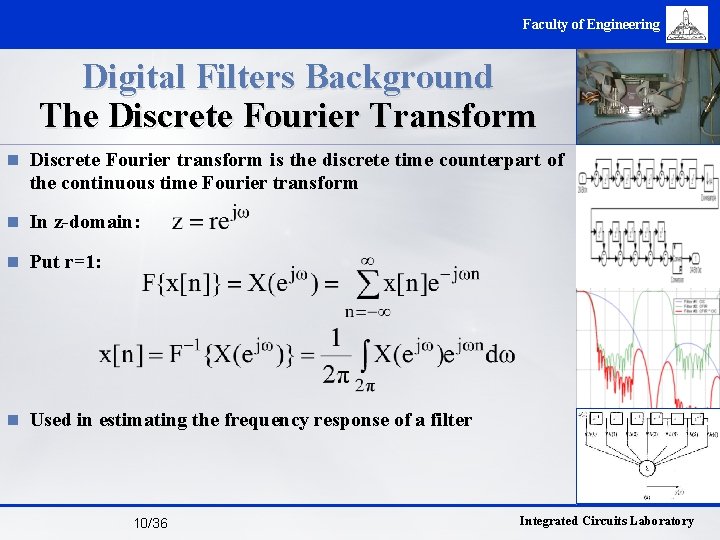
Faculty of Engineering Digital Filters Background The Discrete Fourier Transform n Discrete Fourier transform is the discrete time counterpart of the continuous time Fourier transform n In z-domain: n Put r=1: n Used in estimating the frequency response of a filter 10/36 Integrated Circuits Laboratory

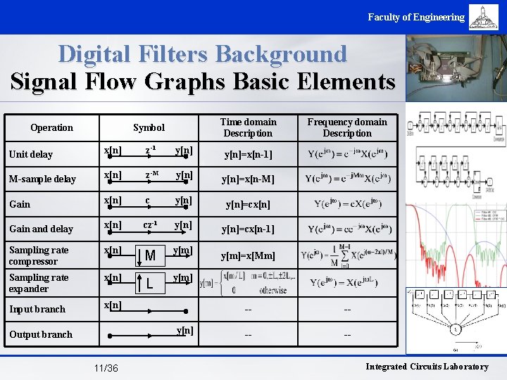
Faculty of Engineering Digital Filters Background Signal Flow Graphs Basic Elements Operation Time domain Description Symbol Unit delay x[n] z-1 y[n]=x[n-1] M-sample delay x[n] z-M y[n]=x[n-M] Gain x[n] c y[n]=cx[n] Gain and delay x[n] cz-1 y[n]=cx[n-1] Sampling rate compressor x[n] M y[m] Sampling rate expander x[n] L y[m] Input branch x[n] y[n] Output branch 11/36 Frequency domain Description y[m]=x[Mm] -- -- -- -Integrated Circuits Laboratory
![Faculty of Engineering Digital Filters Background Signal Flow Graphs Operations x 1n xn ynx Faculty of Engineering Digital Filters Background Signal Flow Graphs Operations x 1[n] x[n] y[n]=x](https://slidetodoc.com/presentation_image_h2/4de2af0e907de6a38ab3ac9d1530def9/image-12.jpg)
Faculty of Engineering Digital Filters Background Signal Flow Graphs Operations x 1[n] x[n] y[n]=x 1[n]+x 2[n]+x 3[n] y[n] x 2[n] x 3[n] z-1 y 1[n]=x[n] y 2[n]=x[n] c 1 c 2 x[n] y[n]=x[n]+c 2 x[n-1]+c 1 y[n-1] y 3[n]=x[n] 12/36 Integrated Circuits Laboratory

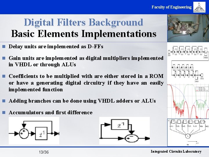
Faculty of Engineering Digital Filters Background Basic Elements Implementations n Delay units are implemented as D-FFs n Gain units are implemented as digital multipliers implemented in VHDL or through ALUs n Coefficients to be multiplied with are either stored in a ROM or have a generating digital circuitry if they have an easily implemented function n Adding branches can be done using VHDL adders or ALUs n Accumulators and first difference 13/36 Integrated Circuits Laboratory

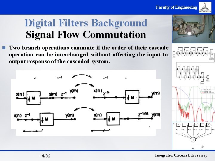
Faculty of Engineering Digital Filters Background Signal Flow Commutation n Two branch operations commute if the order of their cascade operation can be interchanged without affecting the input-tooutput response of the cascaded system. 14/36 Integrated Circuits Laboratory

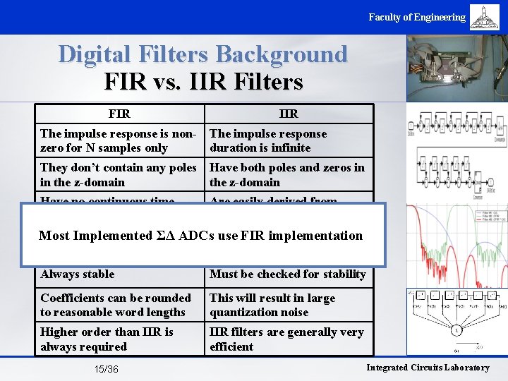
Faculty of Engineering Digital Filters Background FIR vs. IIR Filters FIR IIR The impulse response is nonzero for N samples only The impulse response duration is infinite They don’t contain any poles in the z-domain Have both poles and zeros in the z-domain Have no continuous time counterpart Are easily derived from continuous time filters Linear. Implemented phase can be easily phase can only be Most ΣΔ ADCs. Linear use FIR implementation achieved approximated Always stable Must be checked for stability Coefficients can be rounded to reasonable word lengths This will result in large quantization noise Higher order than IIR is always required IIR filters are generally very efficient 15/36 Integrated Circuits Laboratory

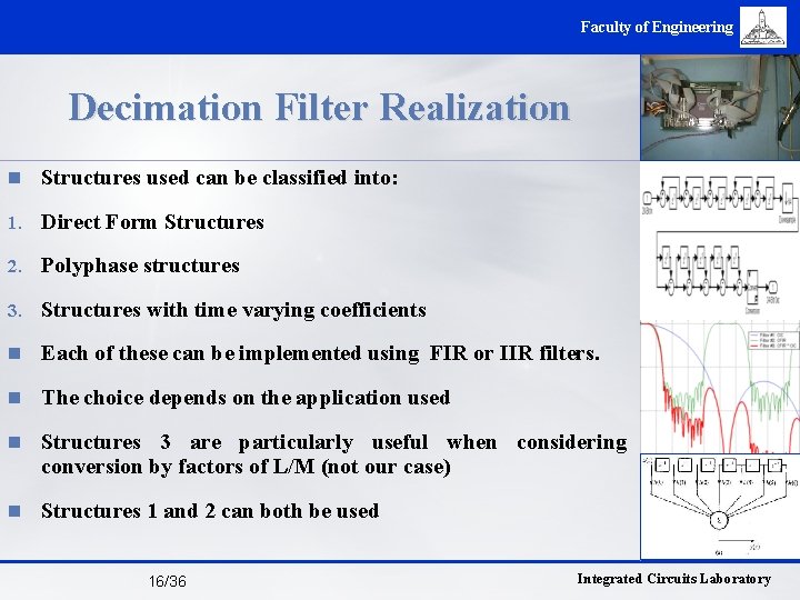
Faculty of Engineering Decimation Filter Realization n Structures used can be classified into: 1. Direct Form Structures 2. Polyphase structures 3. Structures with time varying coefficients n Each of these can be implemented using FIR or IIR filters. n The choice depends on the application used n Structures 3 are particularly useful when considering conversion by factors of L/M (not our case) n Structures 1 and 2 can both be used 16/36 Integrated Circuits Laboratory

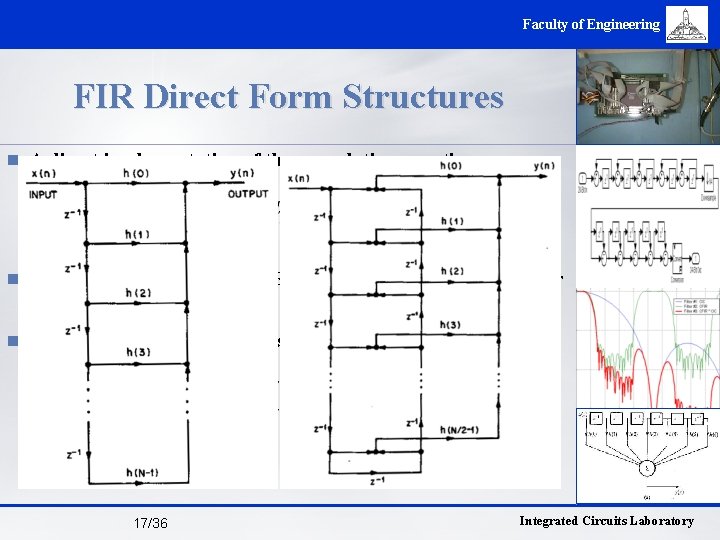
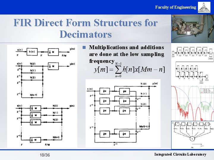
Faculty of Engineering FIR Direct Form Structures n A direct implementation of the convolution equation n In many applications the FIR filter is designed to have linear phase n Consequently, the impulse response is symmetric 17/36 Integrated Circuits Laboratory

Faculty of Engineering FIR Direct Form Structures for Decimators n Multiplications and additions are done at the low sampling frequency 18/36 Integrated Circuits Laboratory

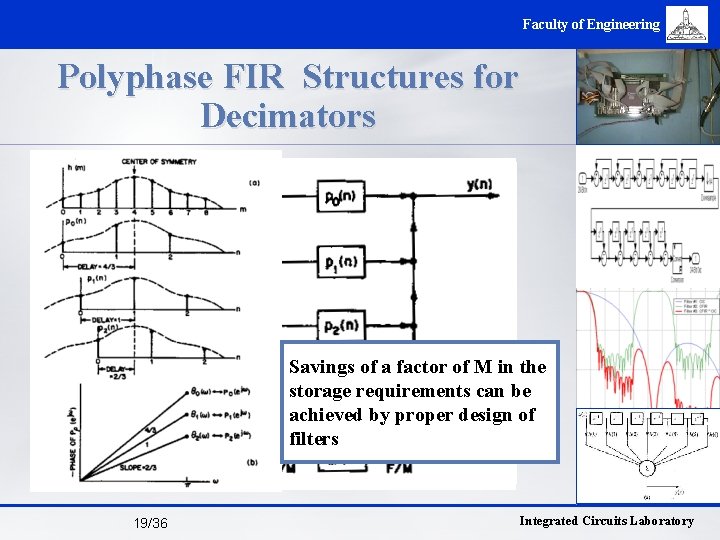
Faculty of Engineering Polyphase FIR Structures for Decimators Savings of a factor of M in the storage requirements can be achieved by proper design of filters 19/36 Integrated Circuits Laboratory

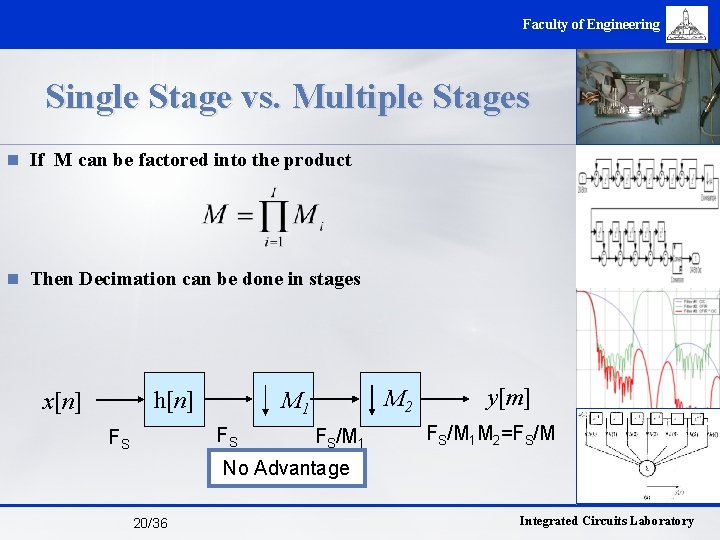
Faculty of Engineering Single Stage vs. Multiple Stages n If M can be factored into the product n Then Decimation can be done in stages h[n] x[n] FS FS M 2 M 1 FS/M 1 y[m] FS/M 1 M 2=FS/M No Advantage 20/36 Integrated Circuits Laboratory

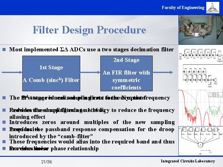
Faculty of Engineering Filter Design Procedure n Most implemented ΣΔ ADCs use a two stages decimation filter 2 nd Stage 1 st Stage A Comb (sinck) Filter An FIR filter with symmetric coefficients nd stage n The 2 first stagereduces is realized sampling as a direct rate to form thestructure Nyquist frequency n Provides Reduces the sampling sharp filtering rate tonecessary 1/16 FS to reduce the frequency n n aliasing effect Introduces zeros around multiples of the new sampling frequencies Provides the passband response compensation for the droop introduced by the “comb-filter” These frequencies would alias into the required band thus increases linear noise phase relationship Provides 21/36 Integrated Circuits Laboratory

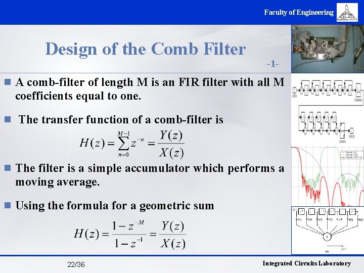
Faculty of Engineering Design of the Comb Filter -1 - n A comb-filter of length M is an FIR filter with all M coefficients equal to one. n The transfer function of a comb-filter is n The filter is a simple accumulator which performs a moving average. n Using the formula for a geometric sum 22/36 Integrated Circuits Laboratory

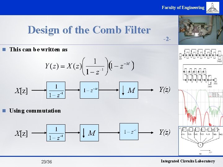
Faculty of Engineering Design of the Comb Filter -2 - n This can be written as M X[z] Y(z) n Using commutation M X[z] 23/36 Y(z) Integrated Circuits Laboratory
![Faculty of Engineering Design of the Comb Filter M Xz 3 Yz n Faculty of Engineering Design of the Comb Filter M X[z] -3 - Y(z) n](https://slidetodoc.com/presentation_image_h2/4de2af0e907de6a38ab3ac9d1530def9/image-24.jpg)
Faculty of Engineering Design of the Comb Filter M X[z] -3 - Y(z) n The accumulation is done at the higher rate n The differentiation is done at the lower rate n 2 registers only are required regardless of M n The filter should be properly scaled for unity gain. This can be done by dividing over M n The two’s complement number system should be used to avoid overflowing 24/36 Integrated Circuits Laboratory

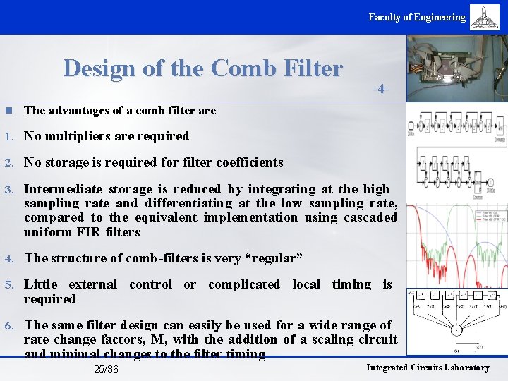
Faculty of Engineering Design of the Comb Filter -4 - n The advantages of a comb filter are 1. No multipliers are required 2. No storage is required for filter coefficients 3. Intermediate storage is reduced by integrating at the high sampling rate and differentiating at the low sampling rate, compared to the equivalent implementation using cascaded uniform FIR filters 4. The structure of comb-filters is very “regular” 5. Little external control or complicated local timing is required 6. The same filter design can easily be used for a wide range of rate change factors, M, with the addition of a scaling circuit and minimal changes to the filter timing 25/36 Integrated Circuits Laboratory

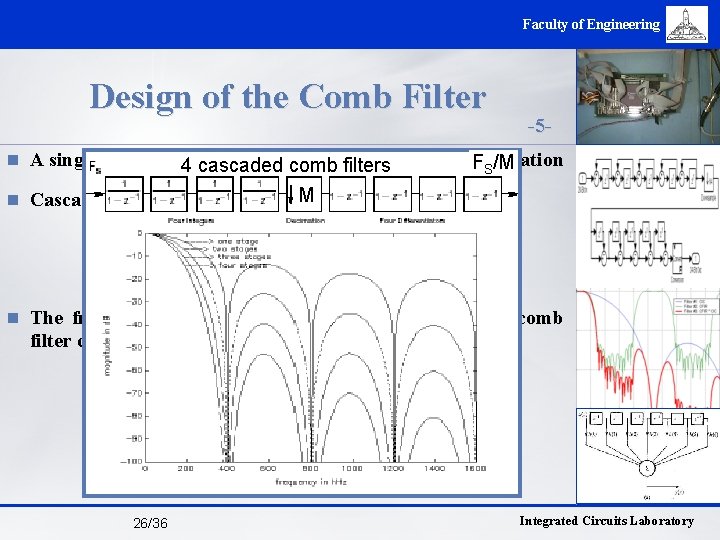
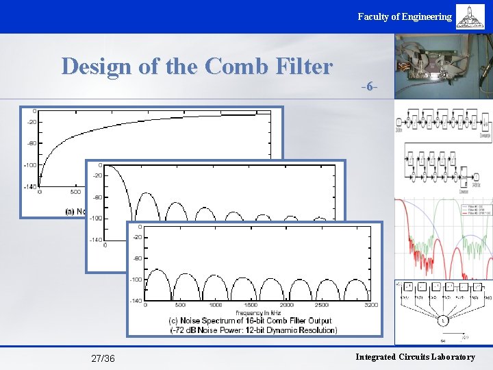
Faculty of Engineering Design of the Comb Filter -5 - n A single comb filter will not give enough stop band attenuation FS/M 4 cascaded comb filters n Cascaded comb filters can often. Mmeet requirements n The frequency response of a properly scaled M stage comb filter can be written as 26/36 Integrated Circuits Laboratory

Faculty of Engineering Design of the Comb Filter 27/36 -6 - Integrated Circuits Laboratory

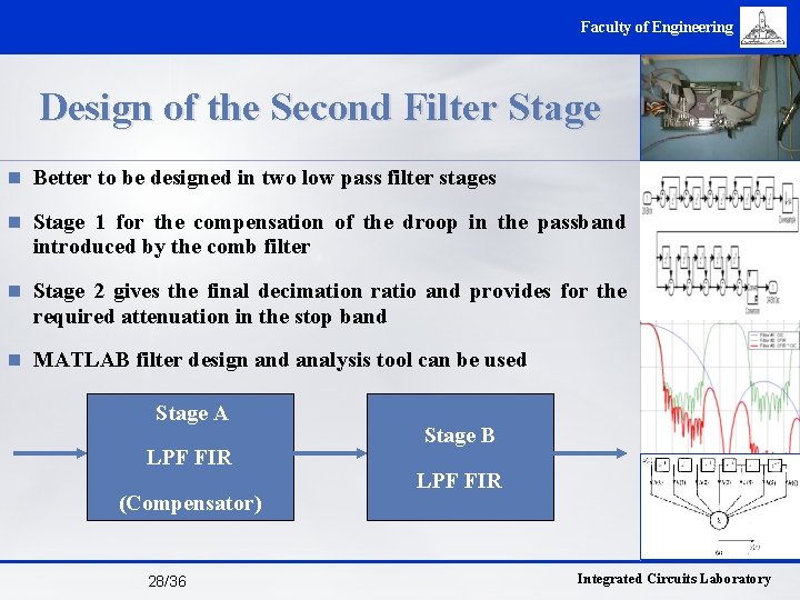
Faculty of Engineering Design of the Second Filter Stage n Better to be designed in two low pass filter stages n Stage 1 for the compensation of the droop in the passband introduced by the comb filter n Stage 2 gives the final decimation ratio and provides for the required attenuation in the stop band n MATLAB filter design and analysis tool can be used Stage A LPF FIR (Compensator) 28/36 Stage B LPF FIR Integrated Circuits Laboratory

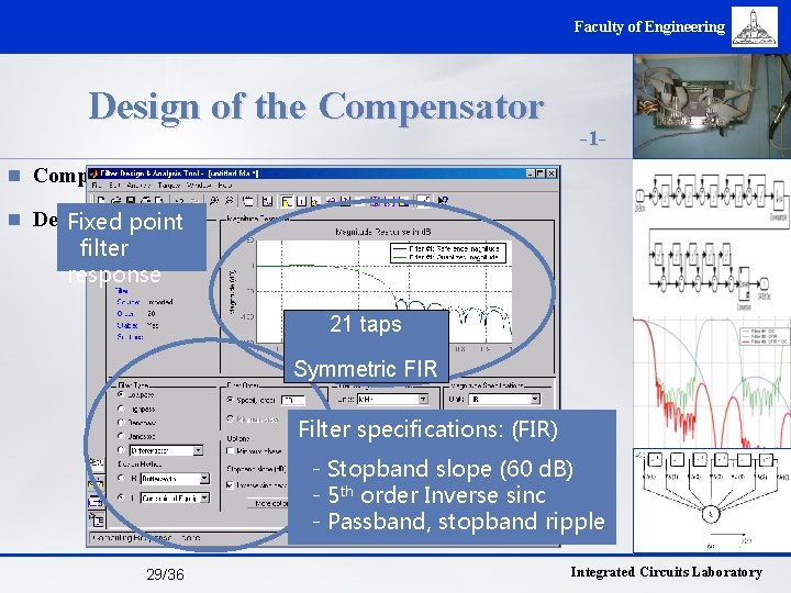
Faculty of Engineering Design of the Compensator -1 - n Compensates the droop of the comb filter n Decimates by 2 Fixed point filter response 21 taps Symmetric FIR Filter specifications: (FIR) - Stopband slope (60 d. B) - 5 th order Inverse sinc - Passband, stopband ripple 29/36 Integrated Circuits Laboratory

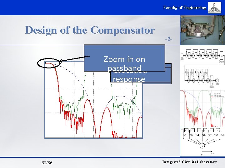
Faculty of Engineering Design of the Compensator -2 - Zoom in on passband Compensation Cascaded Comb filter response added 30/36 Integrated Circuits Laboratory

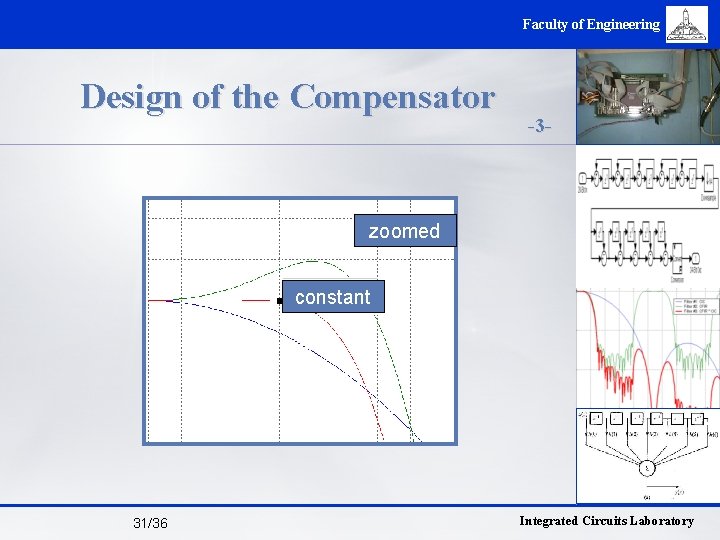
Faculty of Engineering Design of the Compensator -3 - zoomed constant 31/36 Integrated Circuits Laboratory

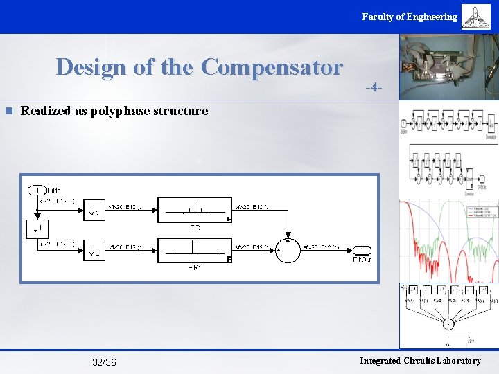
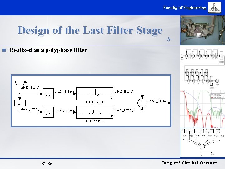
Faculty of Engineering Design of the Compensator -4 - n Realized as polyphase structure 32/36 Integrated Circuits Laboratory

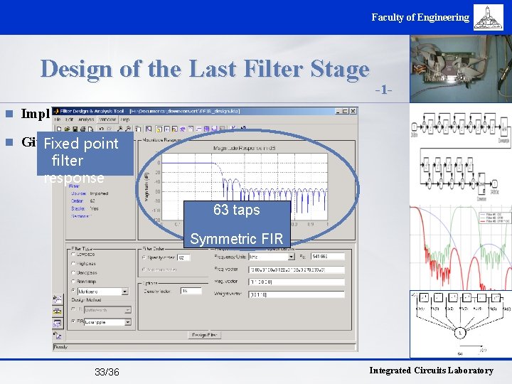
Faculty of Engineering Design of the Last Filter Stage -1 - n Implemented as an FIR LPF n Gives the final Fixed pointattenuation in the stopband required filter response 63 taps Symmetric FIR 33/36 Integrated Circuits Laboratory

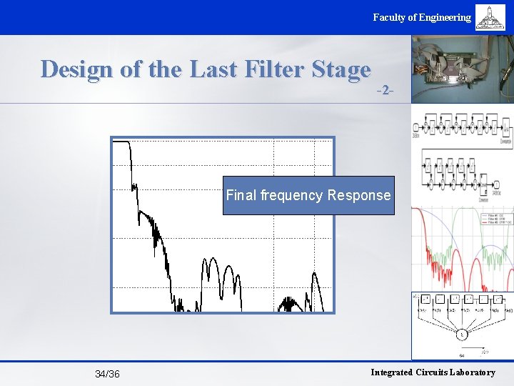
Faculty of Engineering Design of the Last Filter Stage -2 - Final frequency Response 34/36 Integrated Circuits Laboratory

Faculty of Engineering Design of the Last Filter Stage -3 - n Realized as a polyphase filter 35/36 Integrated Circuits Laboratory

Faculty of Engineering References 1. R. E. Crochiere, L. R. Rabiner, “Multirate Digital Signal Processing”, Prentice-Hall, 1983 2. J. C. Candy, G. C. Temes, “Oversampling Delta-Sigma Data Converters, Theory, Design and Simulation”, IEEE Press, 1992 3. D. Orifino, “Designing Digital Radio Applications with Simulink®”, The Math. Works, 2002 4. “Principles of Sigma-Delta Modulation for Analog to Digital Converters”, Motorola 36/36 Integrated Circuits Laboratory