Fabrication Process Crystal Growth Doping Deposition Patterning Lithography
Fabrication Process • Crystal Growth • Doping • Deposition • Patterning • Lithography • Oxidation • Ion Implementation 1
Fabrication- CMOS Process Starting Material Preparation 1. Produce Metallurgical Grade Silicon (MGS) Si. O 2 (sand) + C in Arc Furnace Si- liquid 98% pure 2. Produce Electronic Grade Silicon (EGS) HCl + Si (MGS) Successive purification by distillation Chemical Vapor Deposition (CVD) 2
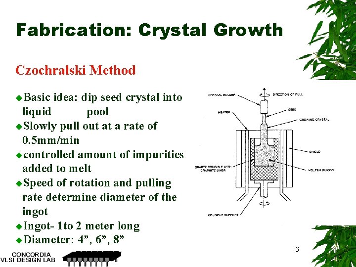
Fabrication: Crystal Growth Czochralski Method u. Basic idea: dip seed crystal into liquid pool u. Slowly pull out at a rate of 0. 5 mm/min ucontrolled amount of impurities added to melt u. Speed of rotation and pulling rate determine diameter of the ingot u. Ingot- 1 to 2 meter long u. Diameter: 4”, 6”, 8” 3
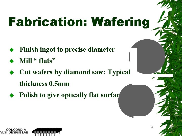
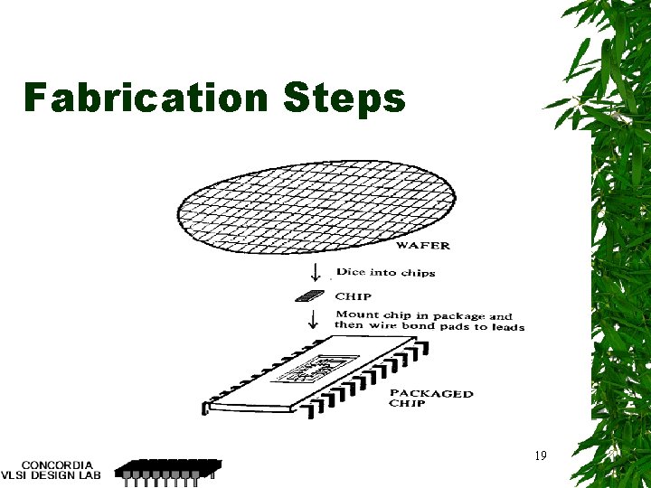
Fabrication: Wafering u Finish ingot to precise diameter u Mill “ flats” u Cut wafers by diamond saw: Typical thickness 0. 5 mm u Polish to give optically flat surface 4
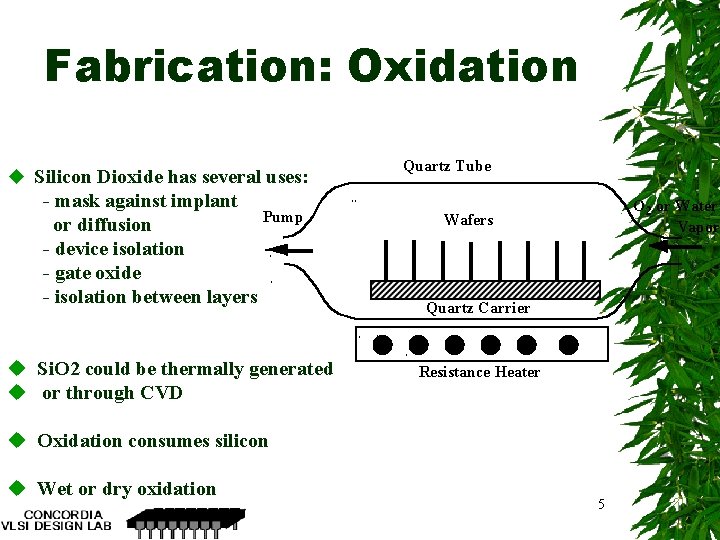
Fabrication: Oxidation u Silicon Dioxide has several uses: - mask against implant Pump or diffusion - device isolation - gate oxide - isolation between layers u Si. O 2 could be thermally generated u or through CVD Quartz Tube O 2 or Water Vapor Wafers Quartz Carrier Resistance Heater u Oxidation consumes silicon u Wet or dry oxidation 5
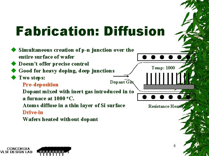
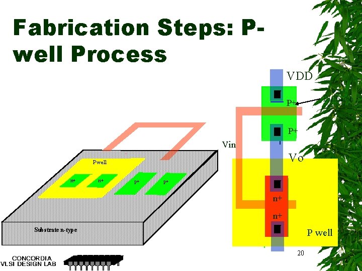
Fabrication: Diffusion u Simultaneous creation of p-n junction over the entire surface of wafer u Doesn’t offer precise control u Good for heavy doping, deep junctions u Two steps: Dopant Gas Pre-deposition Dopant mixed with inert gas introduced in to a furnace at 1000 o. C. Atoms diffuse in a thin layer of Si surface Drive-in Wafers heated without dopant Temp: 1000 wafers Resistance Heater 6
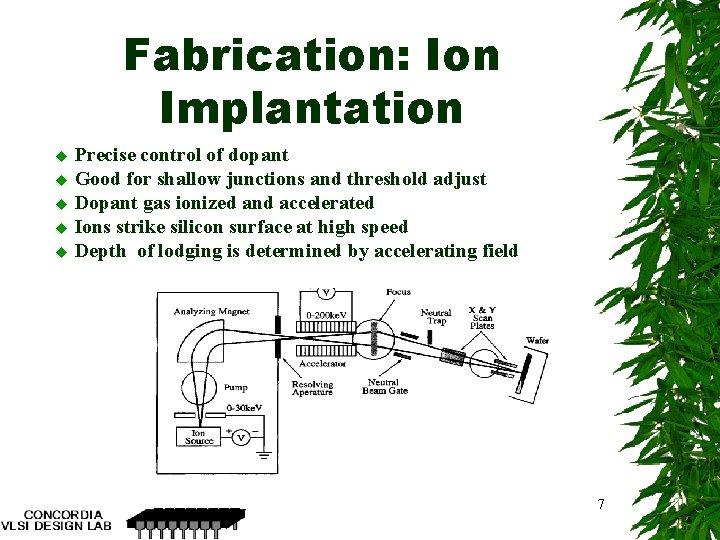
Fabrication: Ion Implantation Precise control of dopant u Good for shallow junctions and threshold adjust u Dopant gas ionized and accelerated u Ions strike silicon surface at high speed u Depth of lodging is determined by accelerating field u 7
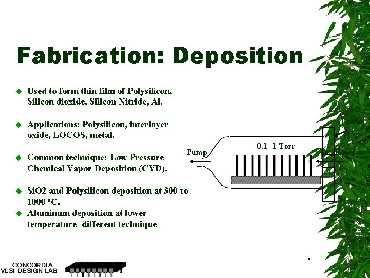
Fabrication: Deposition u Used to form thin film of Polysilicon, Silicon dioxide, Silicon Nitride, Al. u Applications: Polysilicon, interlayer oxide, LOCOS, metal. Loader Pump u Common technique: Low Pressure Chemical Vapor Deposition (CVD). u Si. O 2 and Polysilicon deposition at 300 to 1000 o. C. Aluminum deposition at lower temperature- different technique u 0. 1 -1 Torr Reactant 8
Fabrication: Metallization u Standard material is Aluminum u Low contact resistance to p-type and n-type u When deposited on Si. O 2, Al 2 O 3 is formed: good adhesive u All wafer covered with Al u Deposition techniques: Vacuum Evaporation Electron Beam Evaporation RF Sputtering u Other materials used in conjunction with or replacement to Al 9
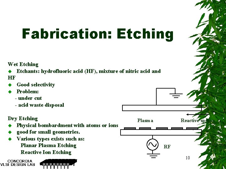
Fabrication: Etching Wet Etching u Etchants: hydrofluoric acid (HF), mixture of nitric acid and HF u Good selectivity u Problem: - under cut - acid waste disposal Dry Etching u Physical bombardment with atoms or ions u good for small geometries. u Various types exists such as: Planar Plasma Etching Reactive Ion Etching Plasma Reactive species RF 10
Fabrication: Lithography Mask making u Most critical part of lithography is conversion from layout to master mask u Masking plate has opaque geometrical shapes corresponding to the area on the wafer surface where certain photochemical reactions have to be prevented or taken place. u Masks uses photographic emulsion or hard surface u Two types: dark field or clear field u Maskmaking: optical or e-beam 11
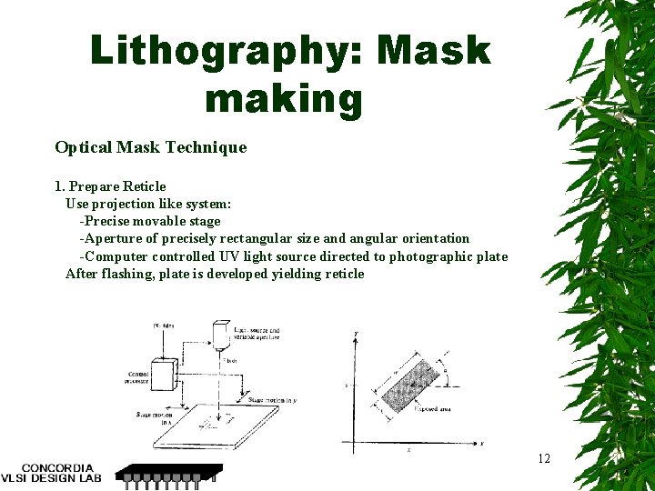
Lithography: Mask making Optical Mask Technique 1. Prepare Reticle Use projection like system: -Precise movable stage -Aperture of precisely rectangular size and angular orientation -Computer controlled UV light source directed to photographic plate After flashing, plate is developed yielding reticle 12
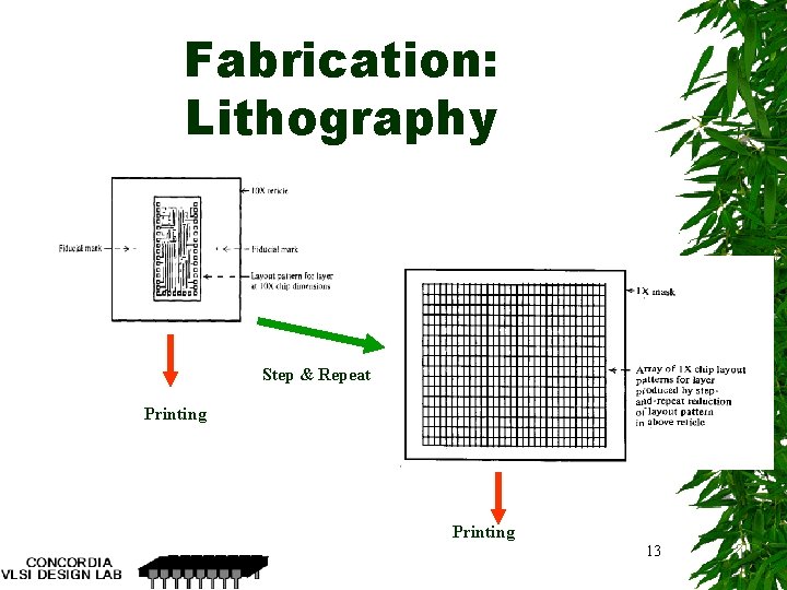
Fabrication: Lithography Step & Repeat Printing 13
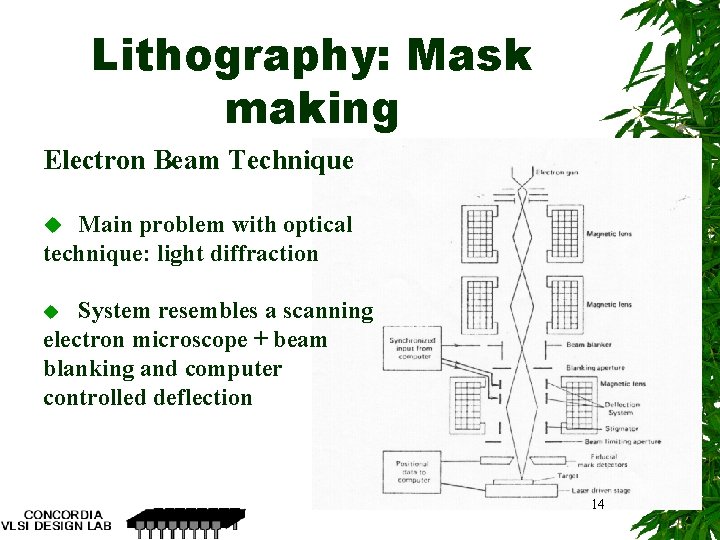
Lithography: Mask making Electron Beam Technique u Main problem with optical technique: light diffraction System resembles a scanning electron microscope + beam blanking and computer controlled deflection u 14
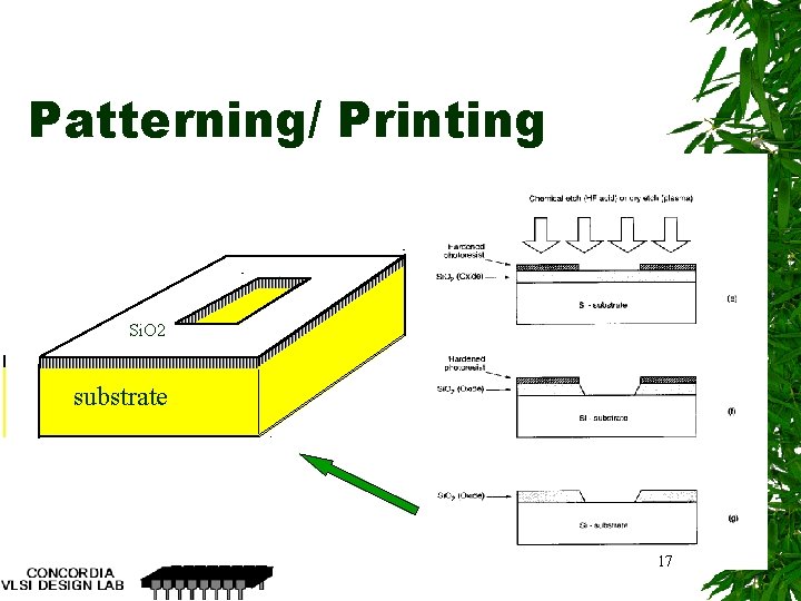
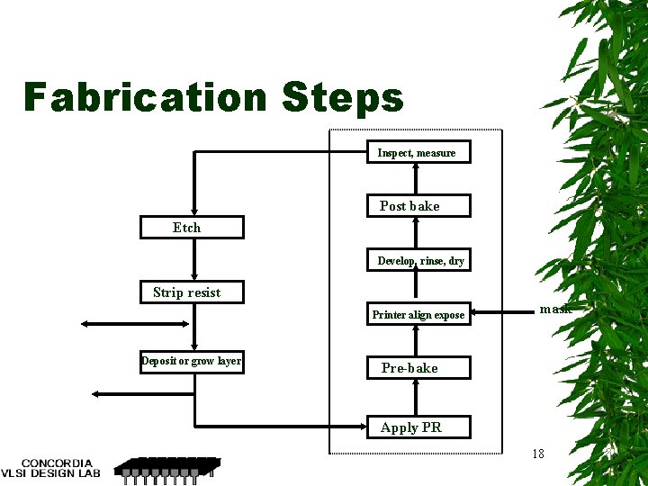
Patterning/ Printing u Process of transferring mask features to surface of the silicon wafer. u u Optical or Electron-beam Photo-resist material (negative or positive): synthetic rubber or polymer upon exposure to light becomes insoluble ( negative ) or volatile (positive) Developer: typically organic solvant-e. g. Xylen A common step in many processes is the creation and selective removal of Silicon Dioxide 15
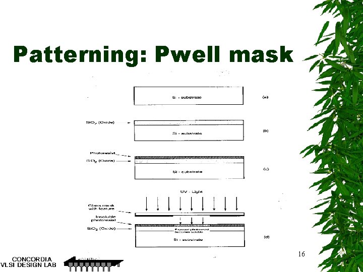
Patterning: Pwell mask 16
Patterning/ Printing Si. O 2 substrate 17
Fabrication Steps Inspect, measure Post bake Etch Develop, rinse, dry Strip resist Printer align expose Deposit or grow layer mask Pre-bake Apply PR 18
Fabrication Steps 19
Fabrication Steps: Pwell Process VDD Diffusion P+ P+ Vin Vo P well n+ n+ p+ p+ n+ n+ Substrate n-type P well 20

Fabrication Steps: Pwell Process VDD Diffusion P+ P+ Vin Vo P well n+ n+ p+ p+ n+ n+ Substrate n-type P well 21
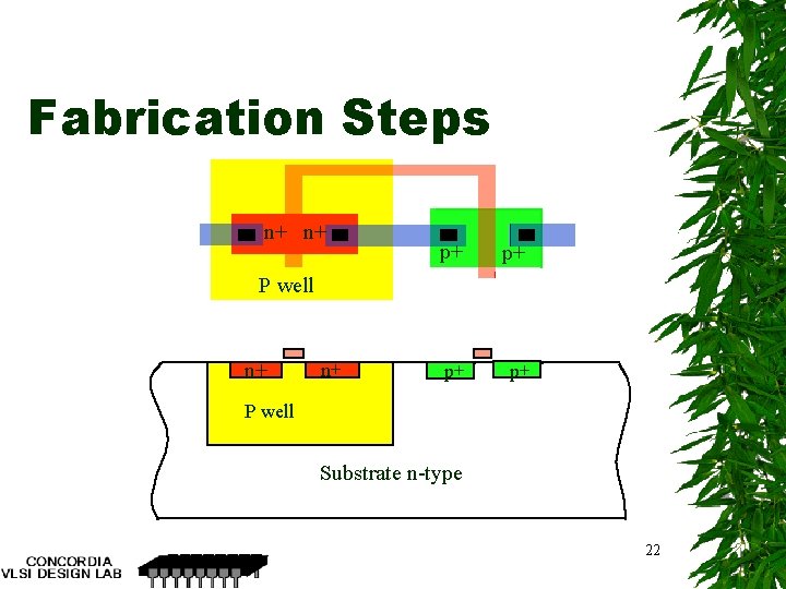
Fabrication Steps n+ n+ p+ p+ P well n+ n+ P well Substrate n-type 22
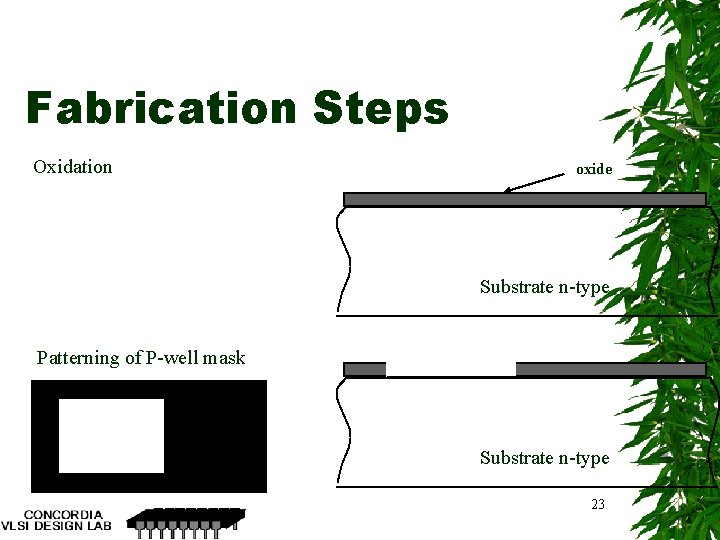
Fabrication Steps Oxidation oxide Substrate n-type Patterning of P-well mask Substrate n-type 23
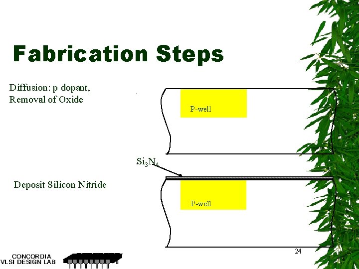
Fabrication Steps Diffusion: p dopant, Removal of Oxide P-well Si 3 N 4 Deposit Silicon Nitride P-well 24
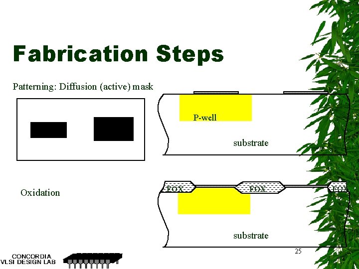
Fabrication Steps Patterning: Diffusion (active) mask P-well substrate Oxidation FOX FOX substrate 25
- Slides: 25