Fabrication of thinfilm In Ga N lightemitting diode

Fabrication of thin-film In. Ga. N lightemitting diode membranes by laser lift-off 2005 -11786 손태홍 2005 -11819 이광희

In. Ga. N/Ga. N DH violet LED ‘ 93 Shuji Nakamura

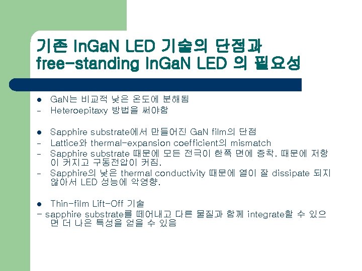
Blue LED에 대한 기존 기술과 그 당시의 대안적이었던 연구 방향 l l l - 기존의 연구 Blue LED의 첫 구현에 사용된 재료는 II-VI compound semiconductor Yoshimoto et al. 의 연구 In. Ga. N를 active layer로 사용하려고 함. Indium의 농도에 따라 1. 9~3. 4 e. V로 bandgap이 조절 가능 Sapphire substrate 위에서 In. Ga. N를 성장시킴 S. nakamura의 연구 In. Ga. N을 Ga. N 층 위에서 성장시키는 것이 더 좋은 특성을 보이는 것을 발견 (crystal quality, external quantum efficiency 측면에서) p-Ga. N/n-In. Ga. N/n-Ga. N의 double hetero structure를 구현 (sapphire substrate 위에서) Two-flow MOCVD 기술 이용
 (1)")
Two-flow MOCVD (metalorganic chemical vapor deposition) (1)
 (3) The crystal quality of the Ga. N")
Two-flow MOCVD (metalorganic chemical vapor deposition) (3) The crystal quality of the Ga. N film was characterized by the double-crystal x-ray rocking curve (XRC) method.

p-Ga. N/n-In. Ga. N/n-Ga. N의 double hetero structure의 구현 l Substrate : Sapphire with (0001) orientation l Trimethylgallium(Ga), trimethylindium(In), Si. H 4(Si), Cp 2 Mg(Mg), NH 3(N) l 성장 시의 각 단계마다 일정한 시간, 온도, gas의 flow rate를 맞춰줌. l Sapphire/Ga. N buffer/Si-doped Ga. N film(n type)/Si-doped In. Ga. N film(n type)/Mg-doped Ga. N film(p type) l p type surface를 부분적으로 etching (n type Ga. N 층이 드러나도록) l 전극을 각 표면에 증착시킴
-based LEDs (II-VI compound)")
In. Ga. N/Ga. N DH violet LED의 특성 Zn( S, Se)-based LEDs (II-VI compound) - 60 μW at a forward current of 20 m. A - the external quantum efficiency 0. 1% - peak wavelength 494 nm l In. Ga. N/Ga. N DH LEDs - 90 μ W at 20 m. A - external quantum efficiency is 0. 15% at 20 m. A - peak wavelength (420 and 411 nm) l l In. Ga. N film을 만들 때에 온도, flow rate 조절을 통해서 In의 비율을 맞 출 수 있고, 따라서 LED에서 나오는 빛의 파장을 바꿀 수 있다.

Thin film In. Ga. N LED by Laser Lift-Off ’ 99 W. S. Wong and T. Sands

Epitaxy와 Multi Quantum Well l l - Heteroepitaxy 보통 스스로 결정성장을 하기 어려운 물질을 성장할 때 쓰는 방 법 다른 결정 위에서 성장시킴 성장 순서 (앞선 s. nakamura 논문에서처럼 MOCVD growth) Sapphire substrate/n-type Ga. N: Si/active region five In. Ga. N QW/p-type Ga. N: Mg chemically assisted ion-beam etching (CAIBE) -> mesa 형 성 전극 증착

Multi Quantum Well l - Quantum well Well : 작은 bandgap Barrier : 큰 bandgap -> quantum well 형성 DOS가 계단모양을 나타내기 때문에 bulk 반도체에서처럼 전자가 비어있는 level을 찾으러 멀리까지 갈 필요가 없음 -> population inversion이 쉽게 일어남 l l l - MQW Quantum well의 효과를 더 넓은 영역에서 확장시킴 DH 와 MQW의 external quantum efficiency 차이 DH : 0. 15% MQW : 1. 7%

Laser Lift-Off 방법의 순서 l l - In. Ga. N LED를 Si wafer에 붙임 ethyl cyanoacrylate (C 6 H 7 NO 2)-based adhesive sapphire/LED/adhesive/Si structure Kr. F pulsed excimer laser sapphire substrate에 대해 pulsed ultraviolet-laser irradiation Ga. N의 short optical absorption length에 의해 film/sapphire interface에 국부적인 가열 가열에 의해 Ga. N이 Ga metal과 N 2 gas로 분해 Ga-rich interfacial layer를 가열해서 녹임 (Tm = 30°C) LED/adhesive/Si structure를 acetone에 담금 - Free-standing membrane 얻음 l
 Effect of LLO on the")
LLO를 거치기 전과 거친 후의 LED 특성 비교 (1) Effect of LLO on the diode junction - I-V curve 가 동일 l l - optical property Shift나 broadening 이 일어나 지 않음
 l - - Power –")
LLO를 거치기 전과 거친 후의 LED 특성 비교 (2) l - - Power – current curve External quantum efficiency 가 1. 7%에서 1. 3%로 감소 Ga. N membrane이 quartz substrate로 옮겨진 이후에 실 험 Poor light coupling Residual absorption or light scattering at the former Ga. N/sapphire interface
- Slides: 16