Fabrication of MEMS Thermal oxidation Thermal Oxidation of

Fabrication of MEMS Thermal oxidation

Thermal Oxidation of silicon � The thermal oxide provides the following: � Passivates and protects the surface of Si � Dielectric material for MOS technology � Mask for diffusion & ion implantation 2

Thermal oxidation of silicon � Si. O 2 can be grown from both dry oxygen and water vapor. � Achieved by heating the silicon wafer to a high temperature (~900 o. C to 1200 o. C) in an atmosphere containing. � The chemical reactions are as follows: � Dry oxygen(dry oxidation) Si + O 2 → Si. O 2 � Water vapor(wet oxidation) Si + 2 H 2 O → Si. O 2 + 2 H 2 3

Thermal oxidation process � Thermal oxidation is a slow process: dry oxidation at 900◦C for 1 h produces ca. 20 nm thick oxide � Wet oxidation for 1 h produces ca. 170 nm thick oxide � 4

Thermal oxidation process
 Max. film")
Comparison between Wet & Dry Oxidation Process details Temprature Dep. Rate (nm/min) Max. film thickness ( m) Density Film stress Dry Wet 1000 -1100 10 30 0 – 0. 2 0 -2 Higher density Lower Density Higher Compressive Lower Compressive

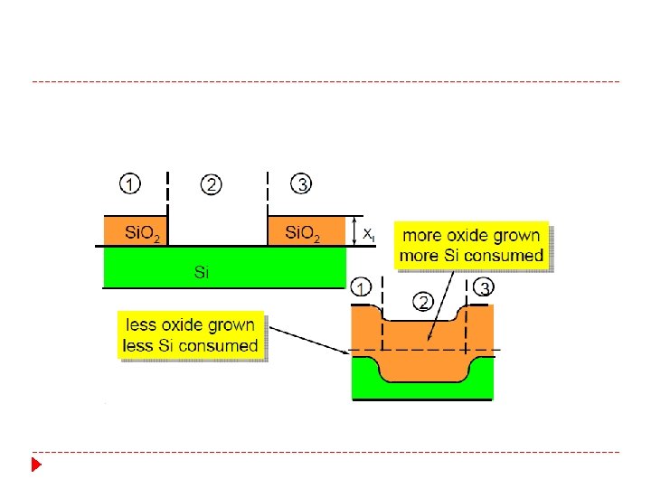
Silicon Consumption � � During the growth of Si. O 2 some of the silicon is consumed. This amount is given by: � Xsi. Nsi = Xox. Nox � � Nox : density of oxide (#/cm ) N : density of silicon X : thickness of Si consumed X : thickness Si. O grown 3 si si ox 2 � Xsi = 0. 46 Xox � The amount of silicon consumed is 46% of the final oxide thickness

Silicon Consumption Original surface Ot 0. 54 Ot 0. 46 Ot

Oxidation Rate Thickness vs. time

Using the Oxidation Growth Charts Growth Chart for <100> Silicon Example: • <100> silicon • Starting oxide thickness: Xi=100 nm • Want to do wet oxidation @ 1000 o. C to achieve Xox=230 nm • What is the time t required for this?

Factors Influencing Thermal Oxidation � Time of oxidation � Temperature of oxidation � Ambient Type (Dry O 2, Steam) � Water vapor : faster oxidation, since water has a higher solubility (i. e. , D) in Si. O 2 than O 2 � Ambient Pressure � Substrate Crystallographic Orientation � <111> ← faster, because there are more bonds available at the Si-surface � <100> ← fewer interface traps; smaller # of unsatisfied Sibonds at the Si-Si. O 2 interface � Substrate Doping

� Conformal �Very Si. O 2 oxide grow on exposed Si surface good etching selectivity between Si and
 � When a portion of a silicon wafer is")
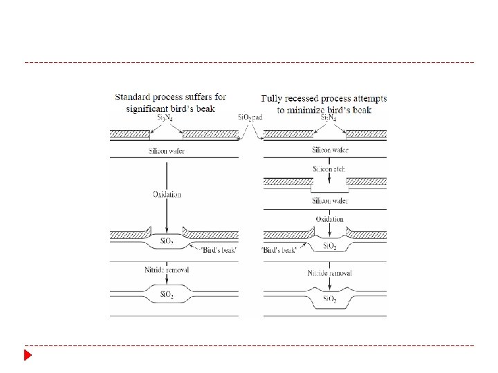
Local Oxidation of Silicon (LOCOS) � When a portion of a silicon wafer is covered with an oxygen diffusion barrier, such as silicon nitride, oxidation cannot occur
")
LOCOS (cont. )

compressive stress � Thermal oxidation of silicon generates compressive stress in the silicon dioxide film. There are two reasons for the stress: Silicon dioxide molecules take more volume than silicon atoms, and there is a mismatch between the coefficients of thermal expansion of silicon and silicon dioxide. The compressive stress depends on the total thickness of the silicon dioxide layer and can reach hundreds of MPa. As a result, thermally grown oxide films cause bowing of the underlying substrate. � Moreover, freestanding membranes and suspended cantilevers made of thermally grown silicon oxide tend to warp or curl due to stress variation through the thickness of the film.
 SOI wafer consists of three layers: A base single-crystal silicon")
SILICON ON INSULATOR (SOI) SOI wafer consists of three layers: A base single-crystal silicon layer or handling wafer; � A buried silicon dioxide (BOX) layer; � The silicon on insulator layer � The thickness of the various layers can be specified when ordering SOI wafers.
 � The thickness of the various layers can be specified")
SILICON ON INSULATOR (SOI) � The thickness of the various layers can be specified when ordering SOI wafers � Two manufacturing processes are available for production of SOI wafers: � SIMOX (Separation by Implantation of Oxygen) � Unibond(BESOI= bonded etched-back silicon on insulator)

SIMOX process for SOI wafers

Unibond process for SOI wafers � This technique uses two polished silicon wafers with an oxide layer on each. The two wafers are then bonded together using fusion bonding. One wafer is then thinned to the desired thickness using chemicalmechanical polishing (CMP)

Unibond process for SOI wafers
- Slides: 22