F R Palomo et al MOS Capacitor DDD
- Slides: 14

F. R. Palomo, et al. MOS Capacitor DDD Dosimeter 1/13 MOS Capacitor Displacement Damage Dose (DDD) Dosimeter F. R. Palomo 1, P. Fernández-Martínez 2 , S. Hidalgo 2, C. Fleta 2, F. Campabadal 2, D. Flores 2 1 Departamento de Ingeniería Electrónica, University of Seville 2 Centro Nacional de Microelectrónica (IMB-CNM-CSIC) RD 50 Workshop - CERN – 14 -16 November 2012

F. R. Palomo, et al. MOS Capacitor DDD Dosimeter 2/13 Outline q Proton Irradiation in MOS Capacitors q HF C-V curves q Radiation Effects in MOS Capacitors q Effect of the Substrate Resistivity q DDD Damage in Sentaurus TCAD q Conclusions: MOS Capacitor DDD Dosimeter RD 50 Workshop - CERN – 14 -16 November 2012

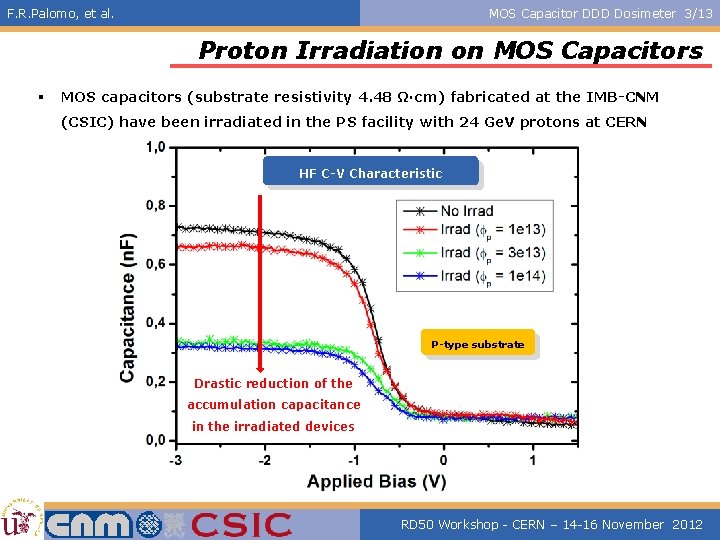
F. R. Palomo, et al. MOS Capacitor DDD Dosimeter 3/13 Proton Irradiation on MOS Capacitors § MOS capacitors (substrate resistivity 4. 48 Ω·cm) fabricated at the IMB-CNM (CSIC) have been irradiated in the PS facility with 24 Ge. V protons at CERN HF C-V Characteristic P-type substrate Drastic reduction of the accumulation capacitance in the irradiated devices RD 50 Workshop - CERN – 14 -16 November 2012

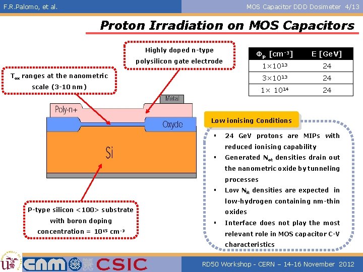
F. R. Palomo, et al. MOS Capacitor DDD Dosimeter 4/13 Proton Irradiation on MOS Capacitors Highly doped n-type Φp [cm-3] E [Ge. V] 1× 10¹³ 24 Tox ranges at the nanometric 3× 10¹³ 24 scale (3 -10 nm) 1× 10¹⁴ 24 polysilicon gate electrode Low ionising Conditions § 24 Ge. V protons are MIPs with reduced ionising capability § Generated Not densities drain out the nanometric oxide by tunneling processes § Low Nit densities are expected in low-hydrogen containing nm-thin P-type silicon <100> substrate with boron doping concentration = 1015 cm-3 oxides § Interface does not play the most relevant role in MOS capacitor C-V characteristics RD 50 Workshop - CERN – 14 -16 November 2012

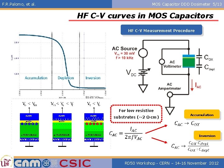
F. R. Palomo, et al. MOS Capacitor DDD Dosimeter 5/13 HF C-V curves in MOS Capacitors HF C-V Measurement Procedure For low resistive Accumulation substrates (~2 Ω·cm) Inversion RD 50 Workshop - CERN – 14 -16 November 2012

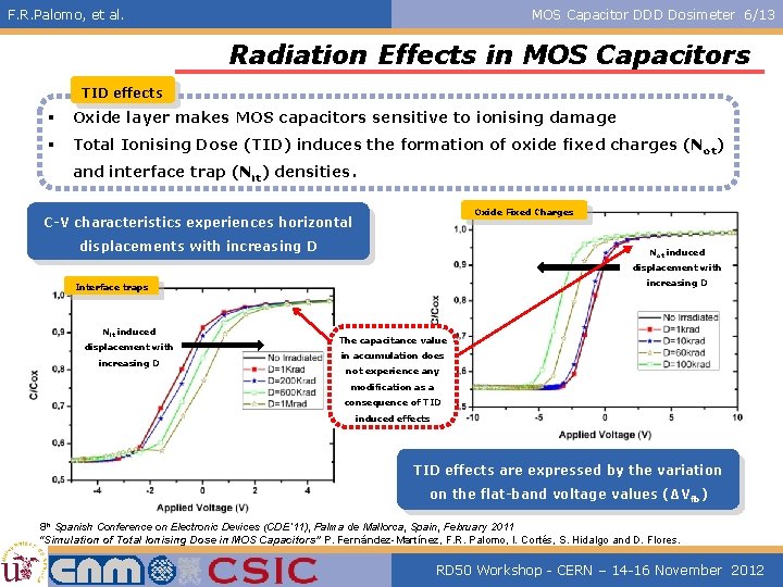
F. R. Palomo, et al. MOS Capacitor DDD Dosimeter 6/13 Radiation Effects in MOS Capacitors TID effects § Oxide layer makes MOS capacitors sensitive to ionising damage § Total Ionising Dose (TID) induces the formation of oxide fixed charges (Not) and interface trap (Nit) densities. Oxide Fixed Charges C-V characteristics experiences horizontal displacements with increasing D Not induced displacement with increasing D Interface traps Nit induced displacement with increasing D The capacitance value in accumulation does not experience any modification as a consequence of TID induced effects TID effects are expressed by the variation on the flat-band voltage values (ΔVfb) 8 th Spanish Conference on Electronic Devices (CDE’ 11), Palma de Mallorca, Spain, February 2011 “Simulation of Total Ionising Dose in MOS Capacitors” P. Fernández-Martínez, F. R. Palomo, I. Cortés, S. Hidalgo and D. Flores. RD 50 Workshop - CERN – 14 -16 November 2012

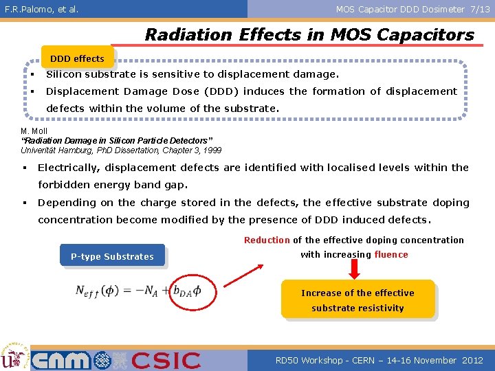
F. R. Palomo, et al. MOS Capacitor DDD Dosimeter 7/13 Radiation Effects in MOS Capacitors DDD effects § Silicon substrate is sensitive to displacement damage. § Displacement Damage Dose (DDD) induces the formation of displacement defects within the volume of the substrate. M. Moll “Radiation Damage in Silicon Particle Detectors” Univerität Hamburg, Ph. D Dissertation, Chapter 3, 1999 § Electrically, displacement defects are identified with localised levels within the forbidden energy band gap. § Depending on the charge stored in the defects, the effective substrate doping concentration become modified by the presence of DDD induced defects. Reduction of the effective doping concentration P-type Substrates with increasing fluence Increase of the effective substrate resistivity RD 50 Workshop - CERN – 14 -16 November 2012

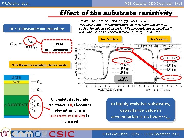
F. R. Palomo, et al. MOS Capacitor DDD Dosimeter 8/13 Effect of the substrate resistivity HF C-V Measurement Procedure Revista Mexicana de Física S 52(2) p. 45 -47, 2006 “Modelling the C-V characteristics of MOS capacitor on high resistivity silicon substrate for PIN photodetector applications”, J. A. Luna-López, M. Aceves-Mijares, O. Malik, R. Glaenzer High Resistivity Low Resistivity Current measurement MOS Capacitor complete electric model N-type substrate Undepleted substrate resistance (Rs) becomes In highly resistive substrates, relevant as long as capacitance value in substrate resistivity is accumulation is no longer Cox increased RD 50 Workshop - CERN – 14 -16 November 2012

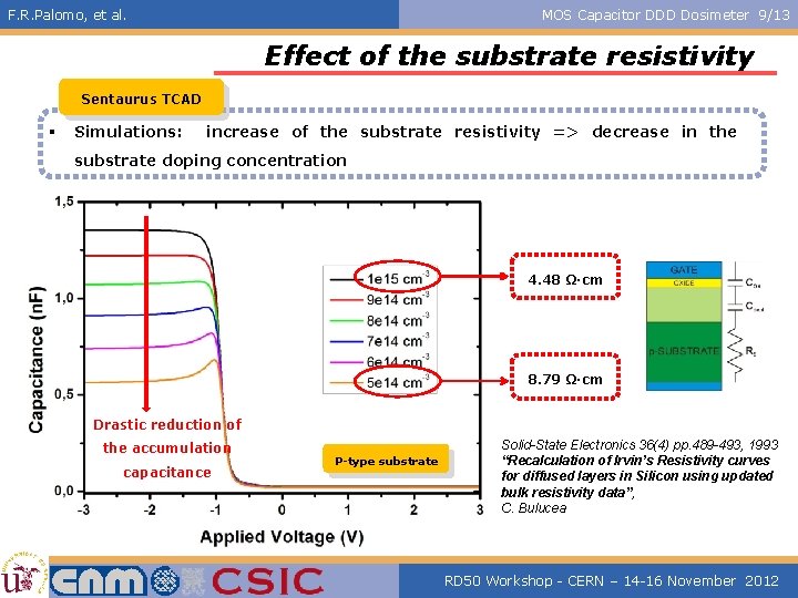
F. R. Palomo, et al. MOS Capacitor DDD Dosimeter 9/13 Effect of the substrate resistivity Sentaurus TCAD § Simulations: increase of the substrate resistivity => decrease in the substrate doping concentration 4. 48 Ω·cm 8. 79 Ω·cm Drastic reduction of the accumulation capacitance P-type substrate Solid-State Electronics 36(4) pp. 489 -493, 1993 “Recalculation of Irvin’s Resistivity curves for diffused layers in Silicon using updated bulk resistivity data”, C. Bulucea RD 50 Workshop - CERN – 14 -16 November 2012

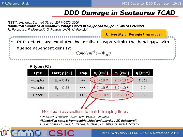
F. R. Palomo, et al. MOS Capacitor DDD Dosimeter 10/13 DDD Damage in Sentaurus TCAD IEEE Trans. Nucl. Sci. , vol. 53, pp. 2971– 2976, 2006 “Numerical Simulation of Radiation Damage Effects in p-Type and n-Type FZ Silicon Detectors”, M. Petasecca, F. Moscatelli, D. Passeri, and G. U. Pignatel University of Perugia trap model § DDD defects are emulated by localised traps within the band-gap, with fluence dependent density: P-type (FZ) Type Energy [e. V] Trap σe [cm 2] σh [cm 2] η [cm-1] Acceptor EC – 0. 42 VV 9. 5× 10 -15 9. 5× 10 -14 1. 613 Acceptor EC – 0. 36 VVV 5. 0× 10 -15 5. 0× 10 -14 0. 9 Donor EC + 0. 36 Ci. Oi 3. 23× 10 -13 3. 23× 10 -14 0. 9 Modified cross sections to match trapping times 10 th RD 50 Workshop, June 2007, Vilnius, Lithuania “Simulation results from double-sided and standard 3 D detectors”, D. Pennicard, C. Fleta, C. Parkes, R. Bates, G. Pellegrini, and M. Lozano RD 50 Workshop - CERN – 14 -16 November 2012

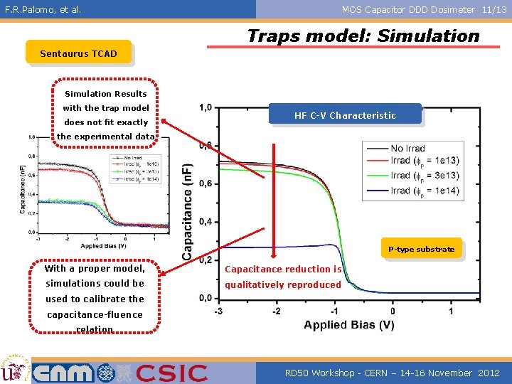
F. R. Palomo, et al. MOS Capacitor DDD Dosimeter 11/13 Traps model: Simulation Sentaurus TCAD Simulation Results with the trap model does not fit exactly HF C-V Characteristic the experimental data P-type substrate With a proper model, Capacitance reduction is simulations could be qualitatively reproduced used to calibrate the capacitance-fluence relation RD 50 Workshop - CERN – 14 -16 November 2012

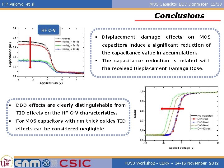
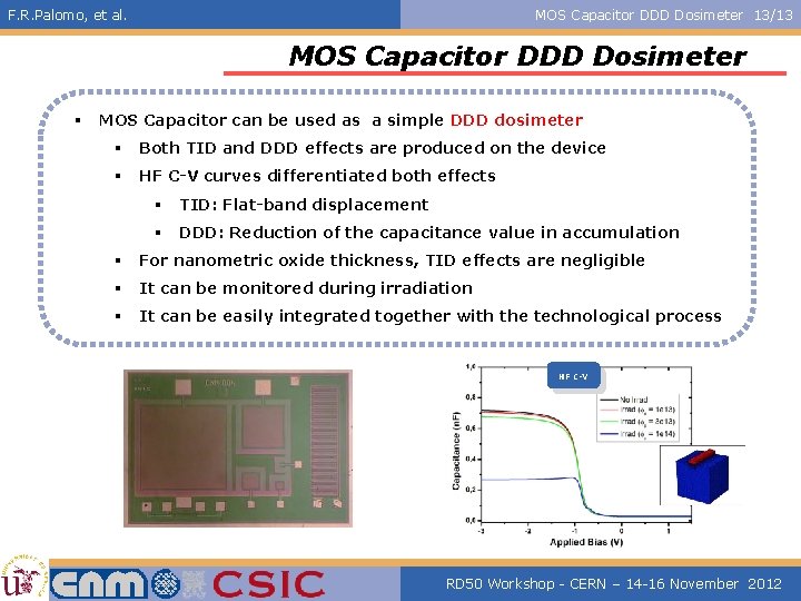
F. R. Palomo, et al. MOS Capacitor DDD Dosimeter 12/13 Conclusions HF C-V § Displacement damage effects on MOS capacitors induce a significant reduction of the capacitance value in accumulation. § The capacitance reduction is related with the received Displacement Damage Dose. § DDD effects are clearly distinguishable from TID effects on the HF C-V characteristics. § For MOS capacitors with nm-thick oxides TID effects can be considered negligible RD 50 Workshop - CERN – 14 -16 November 2012

F. R. Palomo, et al. MOS Capacitor DDD Dosimeter 13/13 MOS Capacitor DDD Dosimeter § MOS Capacitor can be used as a simple DDD dosimeter § Both TID and DDD effects are produced on the device § HF C-V curves differentiated both effects § TID: Flat-band displacement § DDD: Reduction of the capacitance value in accumulation § For nanometric oxide thickness, TID effects are negligible § It can be monitored during irradiation § It can be easily integrated together with the technological process HF C-V RD 50 Workshop - CERN – 14 -16 November 2012

F. R. Palomo, et al. MOS Capacitor DDD Dosimeter 14/13 Thanks for your Attention rogelio@gte. esi. us. es School of Engineering, University of Sevilla, Spain RD 50 Workshop - CERN – 14 -16 November 2012