Exponential Challenges Exponential Rewards The Future of Moores







- Slides: 49

Exponential Challenges, Exponential Rewards— The Future of Moore’s Law Shekhar Borkar Intel Fellow Circuit Research, Intel Labs Fall, 2004 ® 1

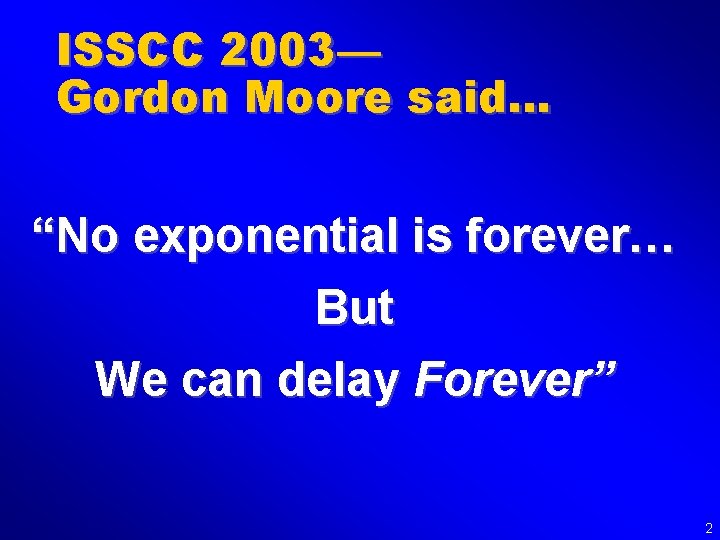
ISSCC 2003— Gordon Moore said… “No exponential is forever… But We can delay Forever” 2

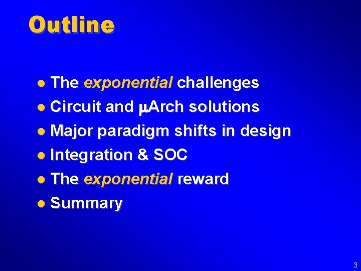
Outline The exponential challenges l Circuit and m. Arch solutions l Major paradigm shifts in design l Integration & SOC l The exponential reward l Summary l 3

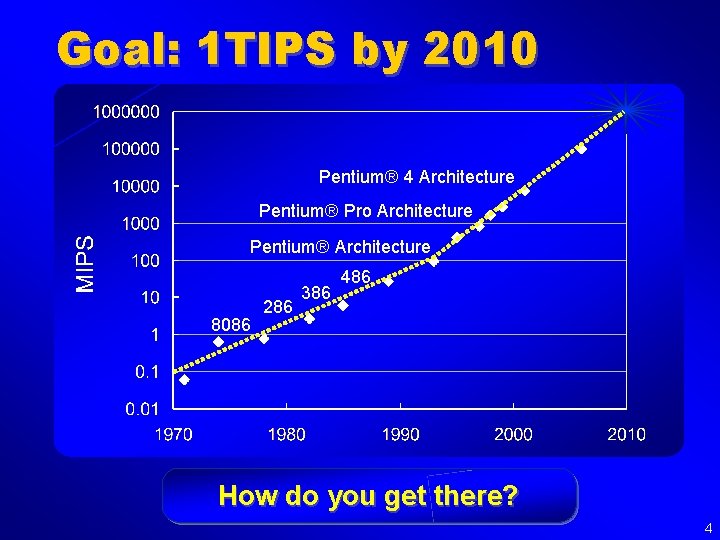
Goal: 1 TIPS by 2010 Pentium® 4 Architecture Pentium® Pro Architecture Pentium® Architecture 8086 286 386 486 How do you get there? 4

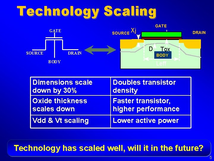
Technology Scaling SOURCE Xj GATE DRAIN SOURCE GATE BODY DRAIN D Tox BODY Leff Dimensions scale down by 30% Oxide thickness scales down Doubles transistor density Faster transistor, higher performance Vdd & Vt scaling Lower active power Technology has scaled well, will it in the future? 5

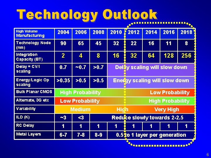
Technology Outlook High Volume Manufacturing Technology Node (nm) Integration Capacity (BT) Delay = CV/I scaling Energy/Logic Op scaling 2004 2006 2008 2010 2012 2014 2016 2018 90 65 45 32 22 16 11 8 2 4 8 16 32 64 128 256 0. 7 ~0. 7 >0. 7 Delay scaling will slow down >0. 35 >0. 5 Energy scaling will slow down Bulk Planar CMOS High Probability Low Probability Alternate, 3 G etc Low Probability High Probability Variability ILD (K) RC Delay Metal Layers Medium High ~3 <3 1 1 1 6 -7 7 -8 8 -9 Very High Reduce slowly towards 2 -2. 5 1 1 1 0. 5 to 1 layer per generation 6

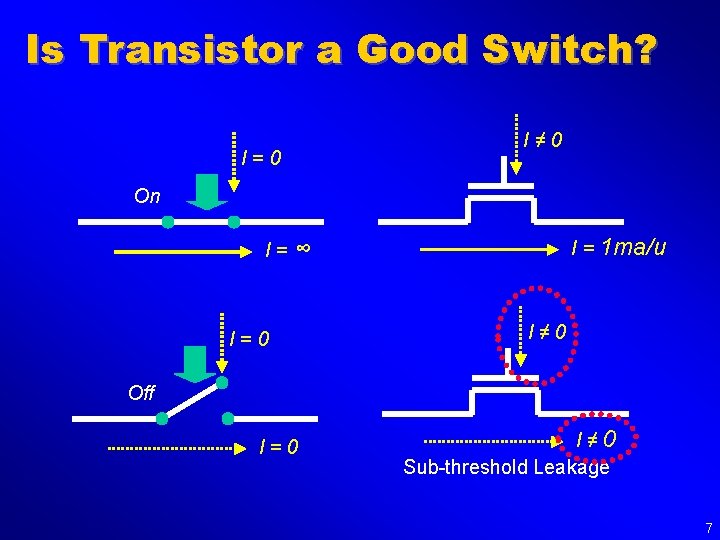
Is Transistor a Good Switch? I=0 I≠ 0 On I = 1 ma/u I=∞ I=0 I≠ 0 Off I=0 I≠ 0 Sub-threshold Leakage 7

Exponential Challenge #1 8

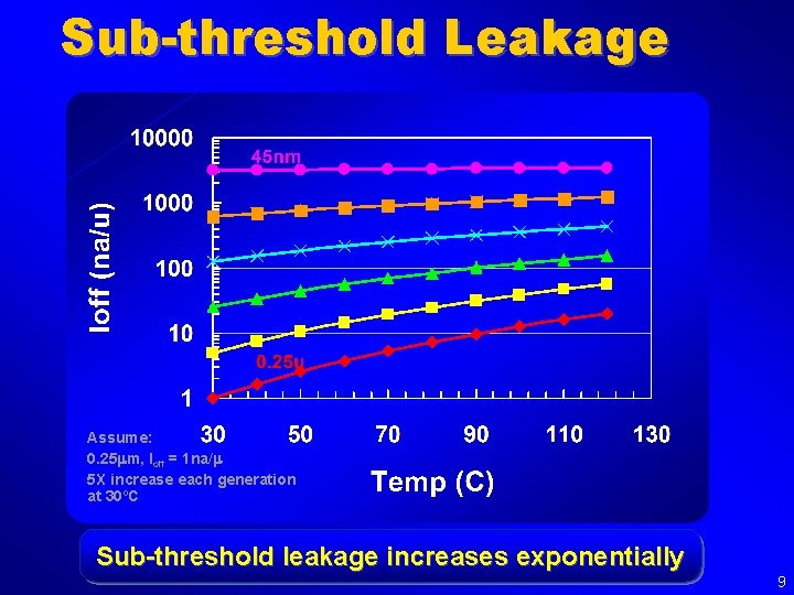
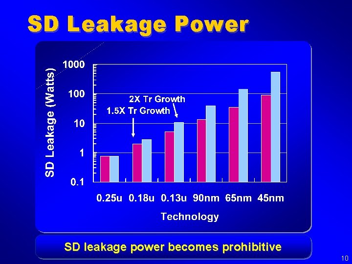
Sub-threshold Leakage Assume: 0. 25 mm, Ioff = 1 na/m 5 X increase each generation at 30ºC Sub-threshold leakage increases exponentially 9

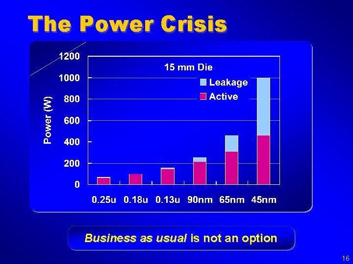
SD Leakage Power SD leakage power becomes prohibitive 10

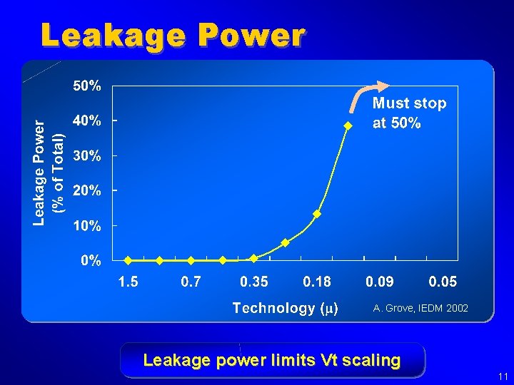
Leakage Power A. Grove, IEDM 2002 Leakage power limits Vt scaling 11

Exponential Challenge #2 12

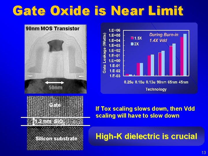
Gate Oxide is Near Limit 90 nm MOS Transistor 50 nm Gate 1. 2 nm Si. O 2 Silicon substrate If Tox scaling slows down, then Vdd scaling will have to slow down High-K dielectric is crucial 13

Exponential Challenge #3 14

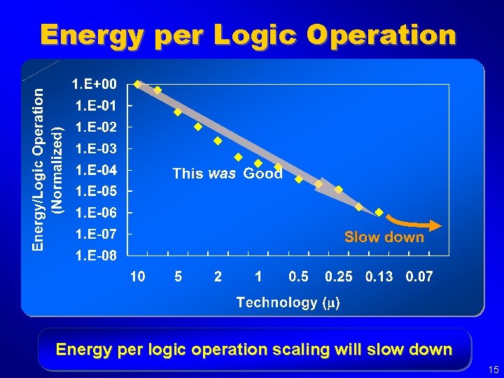
Energy per Logic Operation Energy per logic operation scaling will slow down 15

The Power Crisis Business as usual is not an option 16

Exponential Challenge #4 17

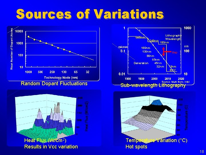
Sources of Variations 365 nm Lithography Wavelength 248 nm 193 nm 180 nm 130 nm Gap 90 nm 65 nm 45 nm Generation 32 nm Random Dopant Fluctuations Heat Flux (W/cm 2) Results in Vcc variation 13 nm EUV Source: Mark Bohr, Intel Sub-wavelength Lithography Temperature Variation (°C) Hot spots 18

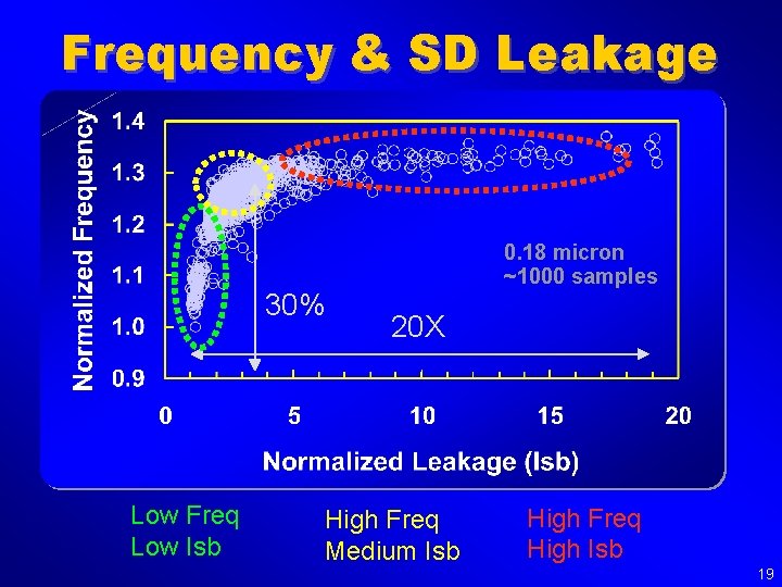
Frequency & SD Leakage 30% Low Freq Low Isb 0. 18 micron ~1000 samples 20 X High Freq Medium Isb High Freq High Isb 19

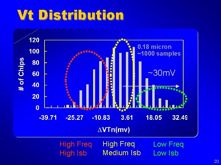
Vt Distribution 0. 18 micron ~1000 samples ~30 m. V High Freq High Isb High Freq Medium Isb Low Freq Low Isb 20

Exponential Challenge #5 21

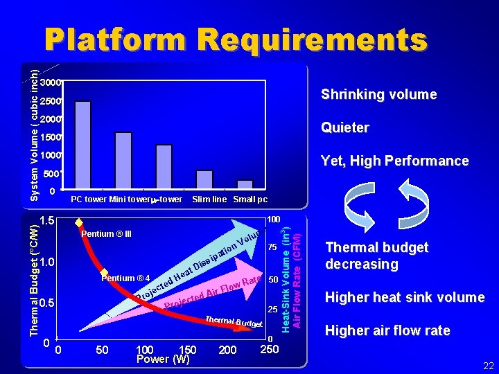
3000 Shrinking volume 2500 2000 Quieter 1500 1000 Yet, High Performance 500 0 PC tower Mini towerm-tower Slim line Small pc Thermal Budget (o. C/W) 1. 5 100 Pentium ® III on 1. 0 ti ipa lu Vo me 75 iss Pentium ® 4 He d cte e oj Pr 0. 5 D at ted ojec Rate 50 w o r Fl Ai Pr 25 Thermal B udget 0 0 50 100 150 Power (W) 200 0 Heat-Sink Volume (in 3) Air Flow Rate (CFM) System Volume ( cubic inch) Platform Requirements Thermal budget decreasing Higher heat sink volume Higher air flow rate 250 22

Exponential Challenge #6 23

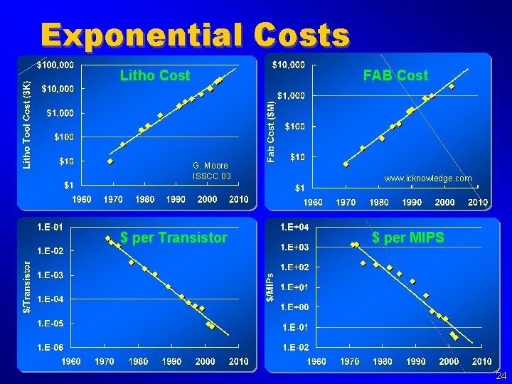
Exponential Costs Litho Cost FAB Cost G. Moore ISSCC 03 $ per Transistor www. icknowledge. com $ per MIPS 24

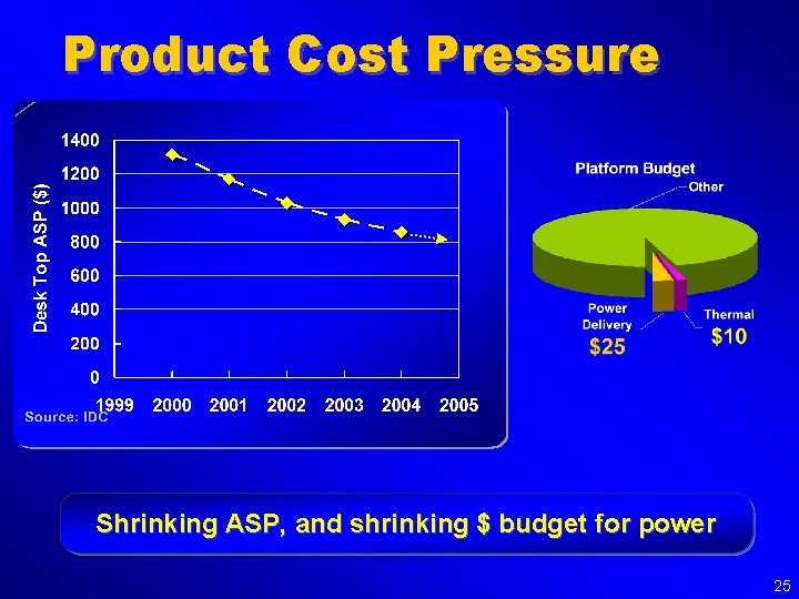
Product Cost Pressure Shrinking ASP, and shrinking $ budget for power 25

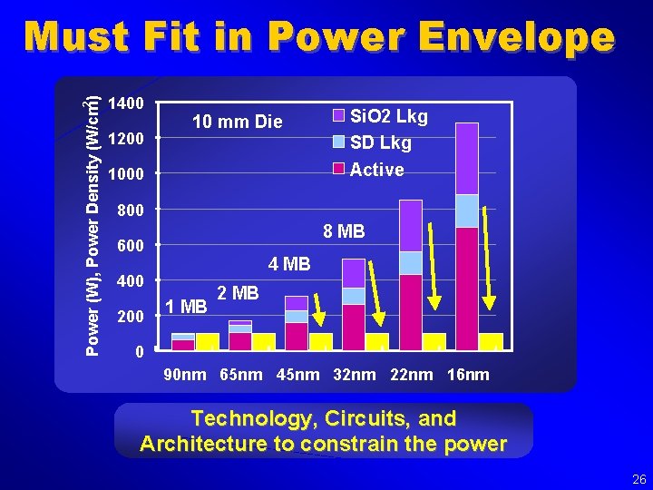
Power (W), Power Density (W/cm 2) Must Fit in Power Envelope 1400 1200 10 mm Die 1000 Si. O 2 Lkg SD Lkg Active 800 8 MB 600 4 MB 400 200 1 MB 2 MB 0 90 nm 65 nm 45 nm 32 nm 22 nm 16 nm Technology, Circuits, and Architecture to constrain the power 26

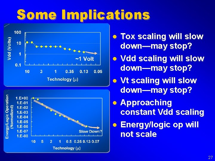
Some Implications l l l Tox scaling will slow down—may stop? Vdd scaling will slow down—may stop? Vt scaling will slow down—may stop? Approaching constant Vdd scaling Energy/logic op will not scale 27

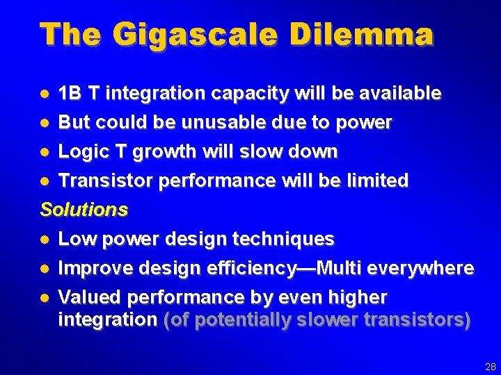
The Gigascale Dilemma l l 1 B T integration capacity will be available But could be unusable due to power Logic T growth will slow down l Transistor performance will be limited Solutions l Low power design techniques l Improve design efficiency—Multi everywhere l Valued performance by even higher integration (of potentially slower transistors) l 28

Power—active and leakage Variations Microarchitecture 29

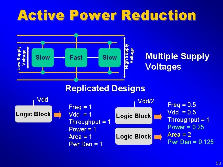
Slow Fast Slow High Supply Voltage Low Supply Voltage Active Power Reduction Multiple Supply Voltages Replicated Designs Vdd Logic Block Vdd/2 Freq = 1 Vdd = 1 Logic Block Throughput = 1 Power = 1 Logic Block Area = 1 Pwr Den = 1 Freq = 0. 5 Vdd = 0. 5 Throughput = 1 Power = 0. 25 Area = 2 Pwr Den = 0. 125 30

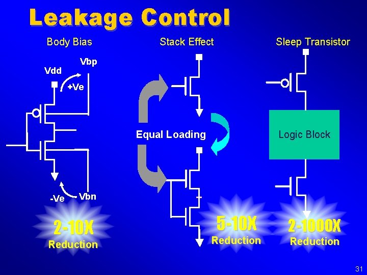
Leakage Control Body Bias Vdd Stack Effect Sleep Transistor Vbp +Ve Equal Loading -Ve Logic Block Vbn 2 -10 X Reduction 5 -10 X Reduction 2 -1000 X Reduction 31

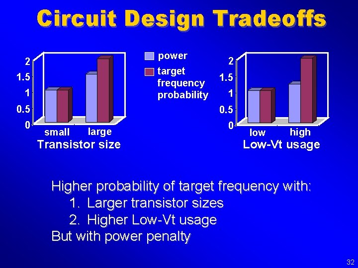
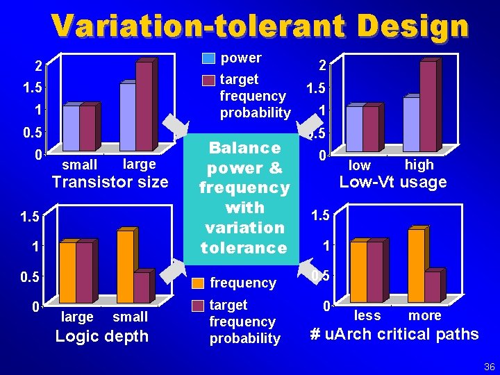
Circuit Design Tradeoffs power 2 target frequency probability 1. 5 1 0. 5 0 2 1. 5 1 0. 5 small large Transistor size 0 low high Low-Vt usage Higher probability of target frequency with: 1. Larger transistor sizes 2. Higher Low-Vt usage But with power penalty 32

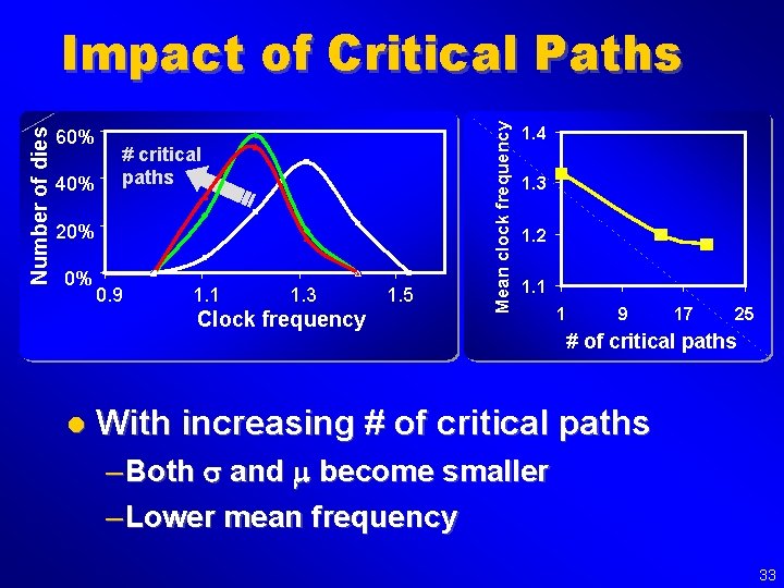
60% 40% # critical paths 20% 0% 0. 9 1. 1 1. 3 Clock frequency l 1. 5 Mean clock frequency Number of dies Impact of Critical Paths 1. 4 1. 3 1. 2 1. 1 1 9 17 25 # of critical paths With increasing # of critical paths – Both s and m become smaller – Lower mean frequency 33

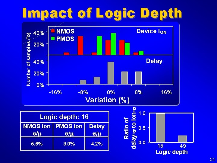
Number of samples (%) Impact of Logic Depth 40% 20% Device ION NMOS PMOS Delay 40% 20% 0% -16% -8% 0% 8% 16% Logic depth: 16 NMOS Ion PMOS Ion s/m s /m 5. 6% 3. 0% Delay s /m 4. 2% Ratio of delay-s to Ion-s Variation (%) 1. 0 0. 5 0. 0 16 49 Logic depth 34

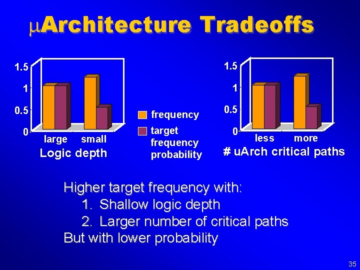
m. Architecture Tradeoffs 1. 5 1 1 0. 5 frequency 0 target frequency probability large small Logic depth 0. 5 0 less more # u. Arch critical paths Higher target frequency with: 1. Shallow logic depth 2. Larger number of critical paths But with lower probability 35

Variation-tolerant Design power 2 target frequency probability 1. 5 1 0. 5 0 small large Transistor size 1. 5 1 Balance power & frequency with variation tolerance 0. 5 frequency 0 target frequency probability large small Logic depth 2 1. 5 1 0. 5 0 low high Low-Vt usage 1. 5 1 0. 5 0 less more # u. Arch critical paths 36

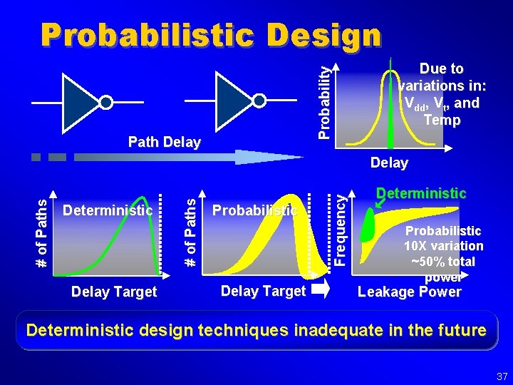
Probability Probabilistic Design Path Delay Due to variations in: Vdd, Vt, and Temp Delay Target Probabilistic Delay Target Frequency Deterministic # of Paths Delay Deterministic Probabilistic 10 X variation ~50% total power Leakage Power Deterministic design techniques inadequate in the future 37

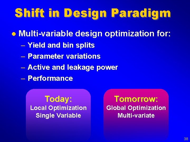
Shift in Design Paradigm l Multi-variable design optimization for: – – Yield and bin splits Parameter variations Active and leakage power Performance Today: Tomorrow: Local Optimization Single Variable Global Optimization Multi-variate 38

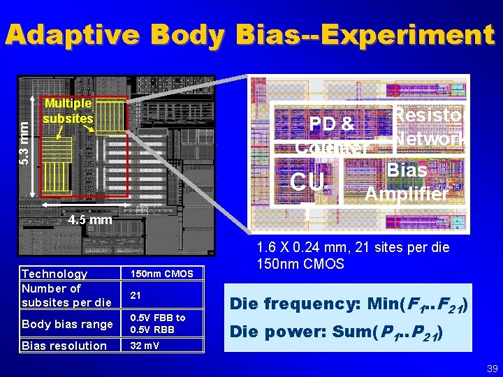
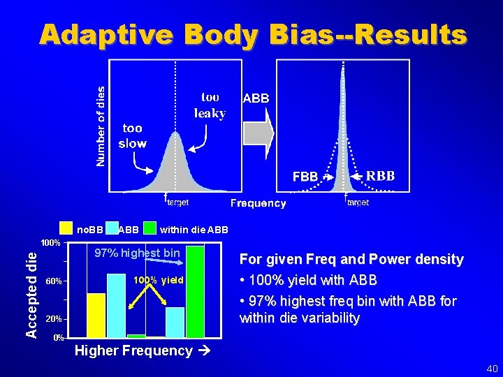
5. 3 mm Adaptive Body Bias--Experiment Multiple subsites Resistor Network 4. 5 mm Technology Number of subsites per die 150 nm CMOS 21 Body bias range 0. 5 V FBB to 0. 5 V RBB Bias resolution 32 m. V PD & Delay Counter CU T Resistor Network Bias Amplifier 1. 6 X 0. 24 mm, 21 sites per die 150 nm CMOS Die frequency: Min(F 1. . F 21) Die power: Sum(P 1. . P 21) 39

Adaptive Body Bias--Results no. BB Accepted die 100% 60% ABB within die ABB 97% highest bin 100% yield • 97% highest freq bin with ABB for within die variability 20% 0% For given Freq and Power density • 100% yield with ABB Higher Frequency 40

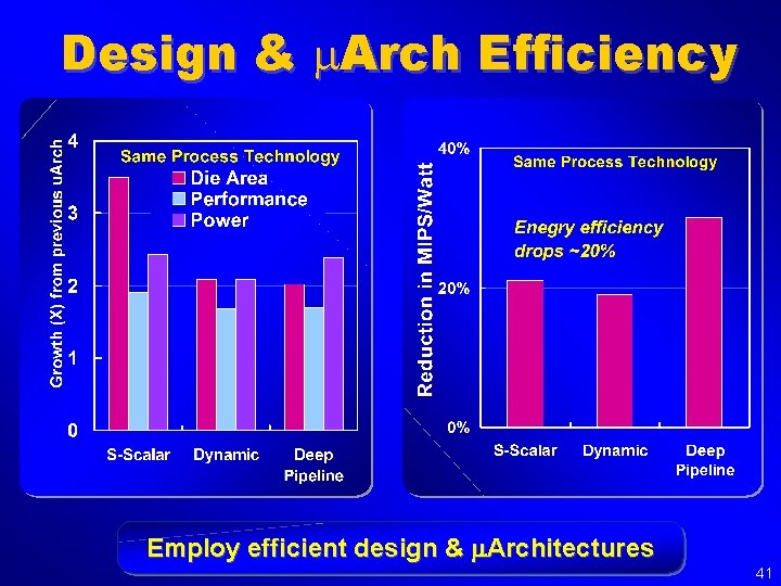
Design & m. Arch Efficiency Employ efficient design & m. Architectures 41

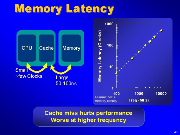
Memory Latency CPU Cache Small ~few Clocks Memory Large 50 -100 ns Assume: 50 ns Memory latency Cache miss hurts performance Worse at higher frequency 42

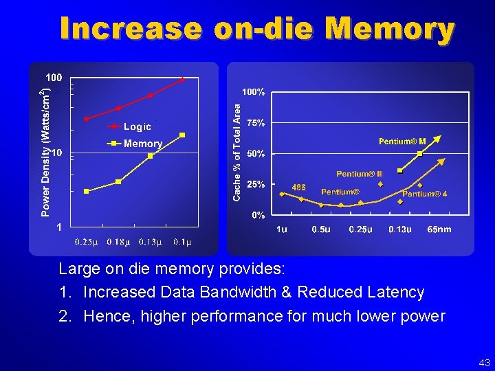
Increase on-die Memory Large on die memory provides: 1. Increased Data Bandwidth & Reduced Latency 2. Hence, higher performance for much lower power 43

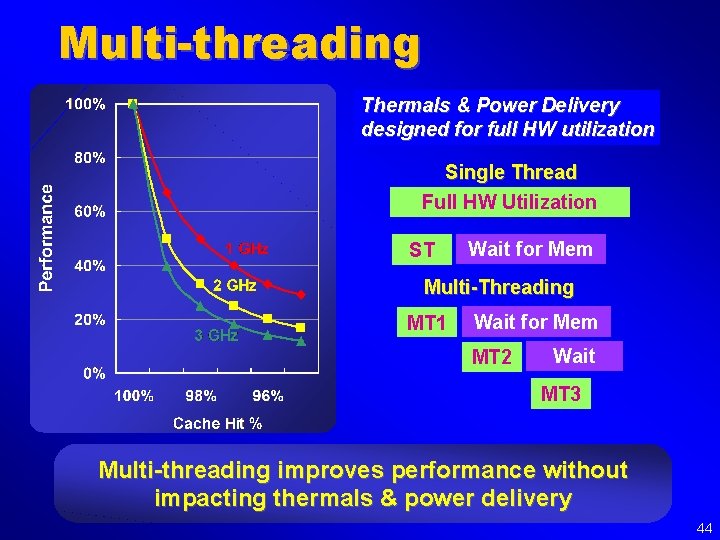
Multi-threading Thermals & Power Delivery designed for full HW utilization Single Thread Full HW Utilization ST Wait for Mem Multi-Threading MT 1 Wait for Mem MT 2 Wait MT 3 Multi-threading improves performance without impacting thermals & power delivery 44

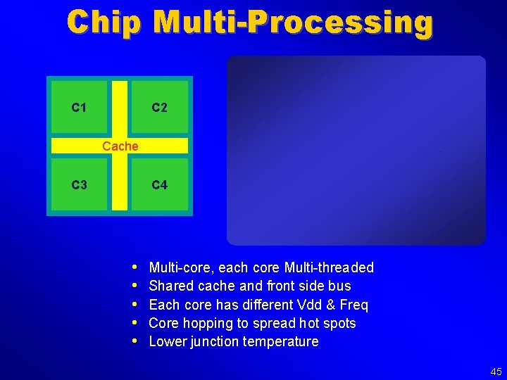
Chip Multi-Processing C 1 C 2 Cache C 3 C 4 • • • Multi-core, each core Multi-threaded Shared cache and front side bus Each core has different Vdd & Freq Core hopping to spread hot spots Lower junction temperature 45

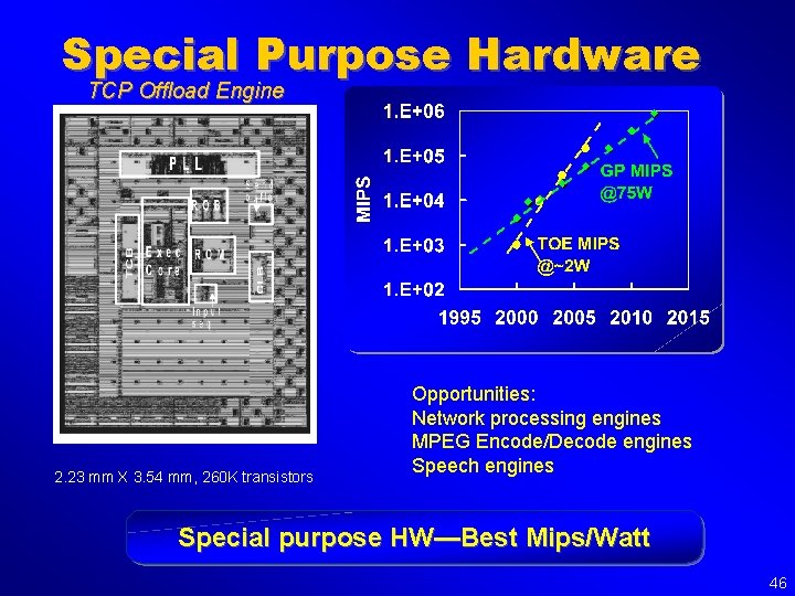
Special Purpose Hardware TCP Offload Engine 2. 23 mm X 3. 54 mm, 260 K transistors Opportunities: Network processing engines MPEG Encode/Decode engines Speech engines Special purpose HW—Best Mips/Watt 46

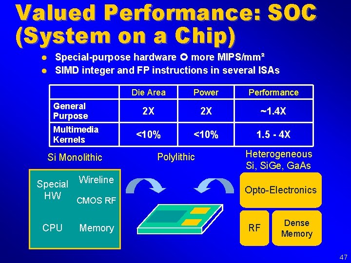
Valued Performance: SOC (System on a Chip) l l Special-purpose hardware more MIPS/mm² SIMD integer and FP instructions in several ISAs General Purpose Multimedia Kernels Si Monolithic Special Wireline HW CMOS RF CPU Memory Die Area Power Performance 2 X 2 X ~1. 4 X <10% 1. 5 - 4 X Polylithic Heterogeneous Si, Si. Ge, Ga. As Opto-Electronics RF Dense Memory 47

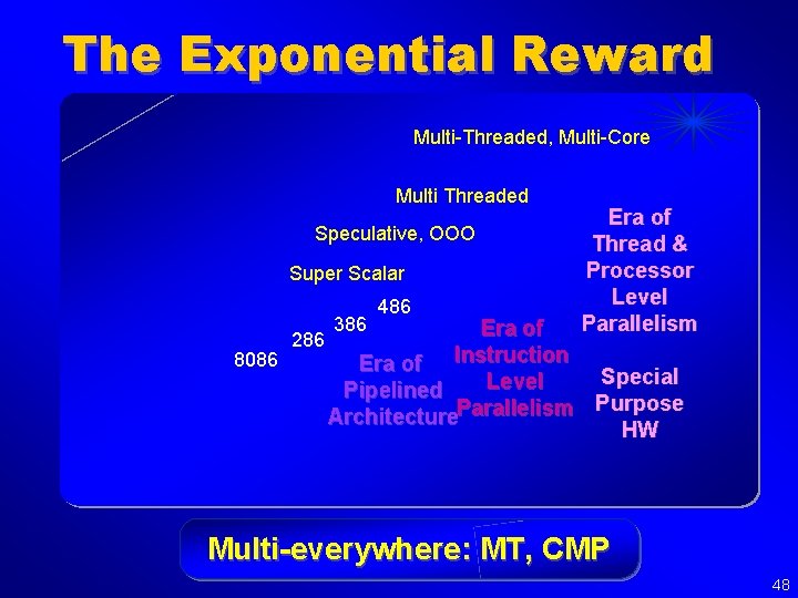
The Exponential Reward Multi-Threaded, Multi-Core Multi Threaded Speculative, OOO Super Scalar 8086 286 386 486 Era of Thread & Processor Level Parallelism Era of Instruction Special Level Pipelined Purpose Architecture. Parallelism HW Multi-everywhere: MT, CMP 48

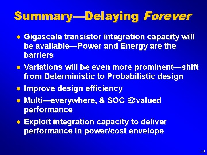
Summary—Delaying Forever l l l Gigascale transistor integration capacity will be available—Power and Energy are the barriers Variations will be even more prominent—shift from Deterministic to Probabilistic design Improve design efficiency Multi—everywhere, & SOC valued performance Exploit integration capacity to deliver performance in power/cost envelope 49