Examples Electrical conductance quantisation Thermal conductance quantisation Single

 From REED’s group at Yale University")

 From IBM Sodium & Iodine on Cu (111)")
 From IBM Fe atoms on Cu(111)")
 From IBM Fe atoms on Cu(111)")
 From IBM Fe atoms on Cu(111)")
 From W. Ho’s group in")
 By varying the size, a enormous range of fundamental properties is")

 Au (50 nm) Ag (90 nm) Ag 40 nm From")


 and New electron sources")


- Slides: 38
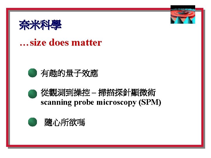
有趣的量子效應 …奈米世界的新定律 Examples: Electrical conductance quantisation Thermal conductance quantisation Single electron charging
掃描穿遂顯微術 (STM) From REED’s group at Yale University
STM pictures From W. Ho’s group in UCI, US
觀測 Xenon atoms on Ni(110) From IBM Sodium & Iodine on Cu (111)
操控 Xenon atoms on Ni(110) From IBM Fe atoms on Cu(111)
量子柵欄 Fe atoms on Cu(111) From IBM Fe atoms on Cu(111)
量子柵欄 Fe atoms on Cu(111) From IBM Fe atoms on Cu(111)
Single-Bond Formation using STM CO and Fe on Ag(110) From W. Ho’s group in UCI, US A=Fe, B=CO, C=Fe. CO, D=Fe(CO)2
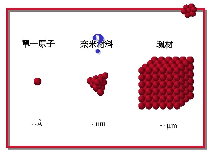
尺度效應 (Size effects) By varying the size, a enormous range of fundamental properties is realized in a material of single chemical component. 導電性 (Electrical conductivity) 光學性質與磁性 (Optical & magnetic properties 硬度與熔點 (Hardness, melting temperature) 催化性質 (Catalytic reactivity and selectivity)
The band gap in Cd. S can be tuned between 4. 5 e. V and 2. 5 e. V as the size is varied from the molecular regime to macroscopic crystal [1]. Silicon clusters containing around 50 atoms emit a strong red light which is not seen in either crytsalline or amorphous forms of silicon [2]. The melting temperature of Cd. S increase from 400 to 1600 C as the size is varied [3]; films made from carbon clusters with 900 atoms behave like graphite, while films made from 20 -atoms clusters behave like diamond [2]. [1] T. Vossmeyer et. al. , J. Phys. Chem. 98 (1994) 7665; [2] R. Palmer, New Scientist 2070 (1997) 38; [3] A. N. Goldstein, Science 256 (1992) 1425.
Ag prism (100 nm) Au (50 nm) Ag (90 nm) Ag 40 nm From C. A. Mirkin’s group in Northwestern University, US Cd. Se nanorod Iron oxide nanocrystal Cd. Se nanorod From A. P. Alivisatos’s group in UC Berkeley, US
Catalytic reactivity and selectivity Bulk Au surfaces are chemically inert, however, supported Au nanoclusters with diameters smaller than 5 nm are active. Propane Au/Ti. O 2 at 80 C Propylene oxide CO + O 2 H 2 + O 2 + Propylene From M. Haruta, Catalysis Today 36 (1997) 153
Au/Ti. O 2 for CO oxidation The placement of nanoparticles in automotive catalytic converters (1) from H. J. Freund et. al. Cryst. Res. Technol. ; (2)Science 299 (2003) 1688
New detectors (sensors) and New electron sources
New building blocks for new materials…
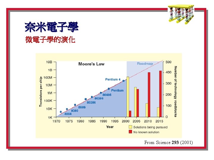
Both microelectronics and nanoelectronics have three levels of organization: 1. The transistor or switch 2. Interconnection—the wires that link transistors 3. Architecture—constructing the circuit From Science 293 (2001)
電晶體與開關 Transistor and switch The conduction path thru a molecular switch is turned on by an applied voltage. The applied voltage is believed to cause a conformational shift which, in concert with the charging of the molecule, opens the conduction pathway. From Mark Reed’s group at Yale University
奈米碳管Carbon nanotubes STM picture of a carbon nanotube 3 d rendered STM image of carbon nanotube Atomic structure of kinked nanotube From Cees Dekker’s group at the Delft University of Technology Artist’s nanotube Transistor
奈米碳管作為電晶體與電線 Carbon nanotube over Pt electrodes AFM image of a nanotube between electrodes 3 d rendered AFM image of kinked nanotube on electrodes From Cees Dekker’s group at the Delft University of Technology
奈米電線 DNA molecule between electrodes AFM image of DNA attached to PNA-derivatized nanotube rope Palladium particle trapped between two electrodes From Cees Dekker’s group at the Delft University of Technology and C. Lieber’s group at Harvard University
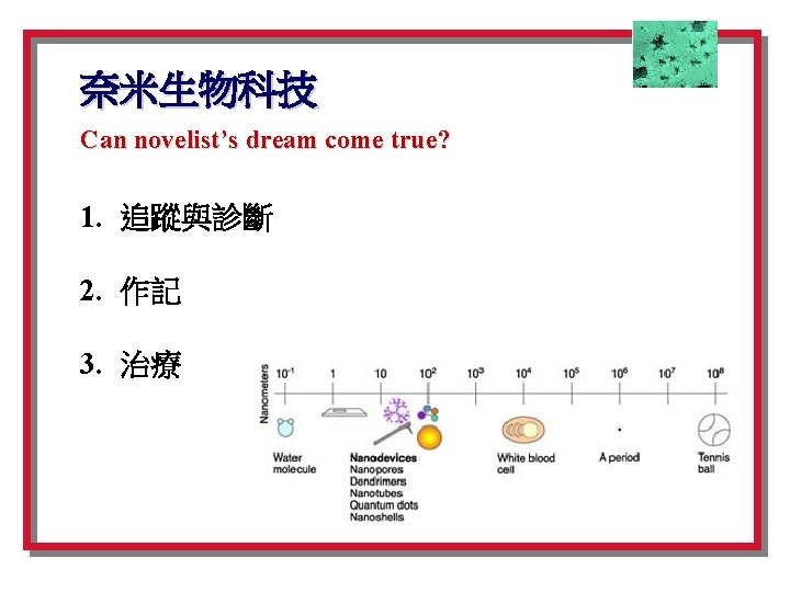
Nanodevices are smaller enough to enter cells… Most animal cells are 10, 000 to 20, 000 nanometers in diameter. This means that nanoscale devices (less than 100 nanometers) can enter cells and the organelles inside them to interact with DNA and proteins.
追蹤與診斷 From National Cancer Institute, US
作記 Quantum dot beads can be used as a spectral bar code to label DNA sequences. Unknown DNA sequences can be revealed by the bar code. To detect cancer, scientists can design quantum dots that bind to sequences of DNA that are associated with the disease. From National Cancer Institute, US
藥物傳送器 One might encapsulate drugs within nanoscale packages and control the medicines’ release in sophisticated ways. Nanoshell attached to a capsule made of a heat-sensitive polymer. From National Cancer Institute, US
Gold nanoshell can absorb near-infrared light which can penetrate several centimeters of tissue. Heating from outside becomes possible. Using gold nanoshell attached to antibodies that bind specifically to tumor cells can destroy the cancerous cells. From National Cancer Institute, US
理想中的奈米機器人 From National Cancer Institute, US