EXAMPLE LED spectral linewidth Solution continued where we

- Slides: 49

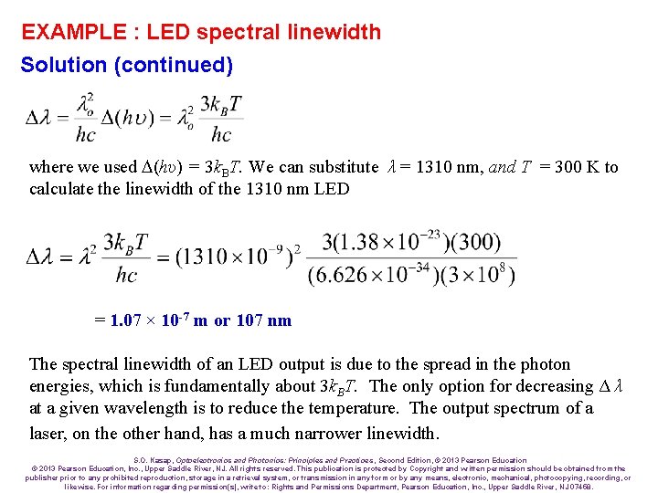
EXAMPLE : LED spectral linewidth Solution (continued) where we used (hυ) = 3 k. BT. We can substitute λ = 1310 nm, and T = 300 K to calculate the linewidth of the 1310 nm LED = 1. 07 × 10 -7 m or 107 nm The spectral linewidth of an LED output is due to the spread in the photon energies, which is fundamentally about 3 k. BT. The only option for decreasing Δ λ at a given wavelength is to reduce the temperature. The output spectrum of a laser, on the other hand, has a much narrower linewidth. S. O. Kasap, Optoelectronics and Photonics: Principles and Practices , Second Edition, © 2013 Pearson Education, Inc. , Upper Saddle River, NJ. All rights reserved. This publication is protected by Copyright and written permission should be obtained from the publisher prior to any prohibited reproduction, storage in a retrieval system, or transmission in any form or by any means, electronic, mechanical, photocopying, recording, or likewise. For information regarding permission(s), write to: Rights and Permissions Department, Pearson Education, Inc. , Upper Saddle River, NJ 07458.

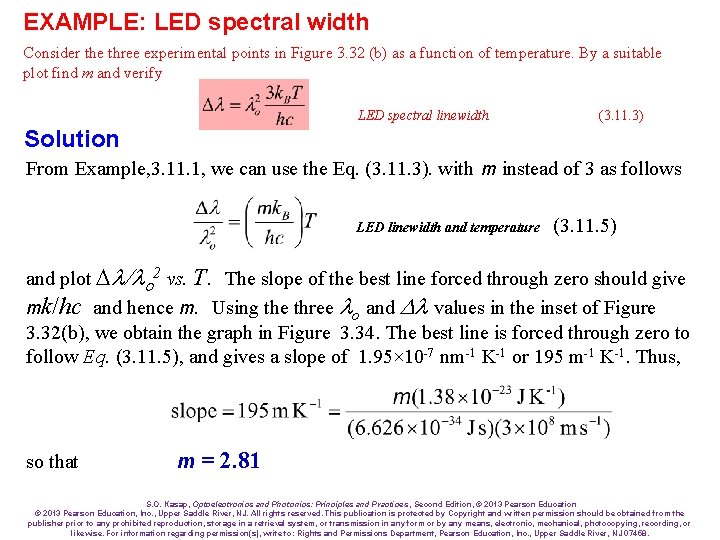
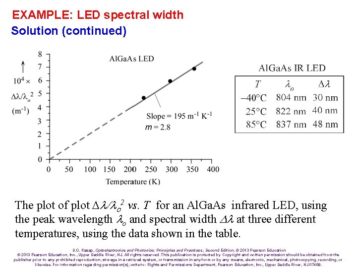
EXAMPLE: LED spectral width Consider the three experimental points in Figure 3. 32 (b) as a function of temperature. By a suitable plot find m and verify LED spectral linewidth (3. 11. 3) Solution From Example, 3. 11. 1, we can use the Eq. (3. 11. 3). with m instead of 3 as follows LED linewidth and temperature (3. 11. 5) and plot / o 2 vs. T. The slope of the best line forced through zero should give mk/hc and hence m. Using the three o and D values in the inset of Figure 3. 32(b), we obtain the graph in Figure 3. 34. The best line is forced through zero to follow Eq. (3. 11. 5), and gives a slope of 1. 95× 10 -7 nm-1 K-1 or 195 m-1 K-1. Thus, so that m = 2. 81 S. O. Kasap, Optoelectronics and Photonics: Principles and Practices , Second Edition, © 2013 Pearson Education, Inc. , Upper Saddle River, NJ. All rights reserved. This publication is protected by Copyright and written permission should be obtained from the publisher prior to any prohibited reproduction, storage in a retrieval system, or transmission in any form or by any means, electronic, mechanical, photocopying, recording, or likewise. For information regarding permission(s), write to: Rights and Permissions Department, Pearson Education, Inc. , Upper Saddle River, NJ 07458.

EXAMPLE: LED spectral width Solution (continued) The plot of plot / o 2 vs. T for an Al. Ga. As infrared LED, using the peak wavelength o and spectral width D at three different temperatures, using the data shown in the table. S. O. Kasap, Optoelectronics and Photonics: Principles and Practices , Second Edition, © 2013 Pearson Education, Inc. , Upper Saddle River, NJ. All rights reserved. This publication is protected by Copyright and written permission should be obtained from the publisher prior to any prohibited reproduction, storage in a retrieval system, or transmission in any form or by any means, electronic, mechanical, photocopying, recording, or likewise. For information regarding permission(s), write to: Rights and Permissions Department, Pearson Education, Inc. , Upper Saddle River, NJ 07458.

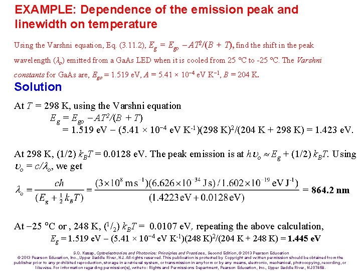
EXAMPLE: Dependence of the emission peak and linewidth on temperature Using the Varshni equation, Eq. (3. 11. 2), Eg = Ego - AT 2/(B + T), find the shift in the peak wavelength (λo) emitted from a Ga. As LED when it is cooled from 25 C to -25 C. The Varshni constants for Ga. As are, Ego = 1. 519 e. V, A = 5. 41 × 10− 4 e. V K− 1, B = 204 K. Solution At T = 298 K, using the Varshni equation Eg = Ego - AT 2/(B + T) = 1. 519 e. V - (5. 41 × 10− 4 e. V K-1)(298 K)2/(204 K + 298 K) = 1. 423 e. V. At 298 K, (1/2) k. BT = 0. 0128 e. V. The peak emission is at h o Eg + (1/2) k. BT. Using o = c/ o, we get = 864. 2 nm At -25 C or , 248 K, (1/2) k. BT = 0. 0107 e. V, repeating the above calculation, Eg = 1. 519 e. V - (5. 41 × 10− 4 e. V K-1)(248 K)2/(204 K + 248 K) = 1. 445 e. V S. O. Kasap, Optoelectronics and Photonics: Principles and Practices , Second Edition, © 2013 Pearson Education, Inc. , Upper Saddle River, NJ. All rights reserved. This publication is protected by Copyright and written permission should be obtained from the publisher prior to any prohibited reproduction, storage in a retrieval system, or transmission in any form or by any means, electronic, mechanical, photocopying, recording, or likewise. For information regarding permission(s), write to: Rights and Permissions Department, Pearson Education, Inc. , Upper Saddle River, NJ 07458.

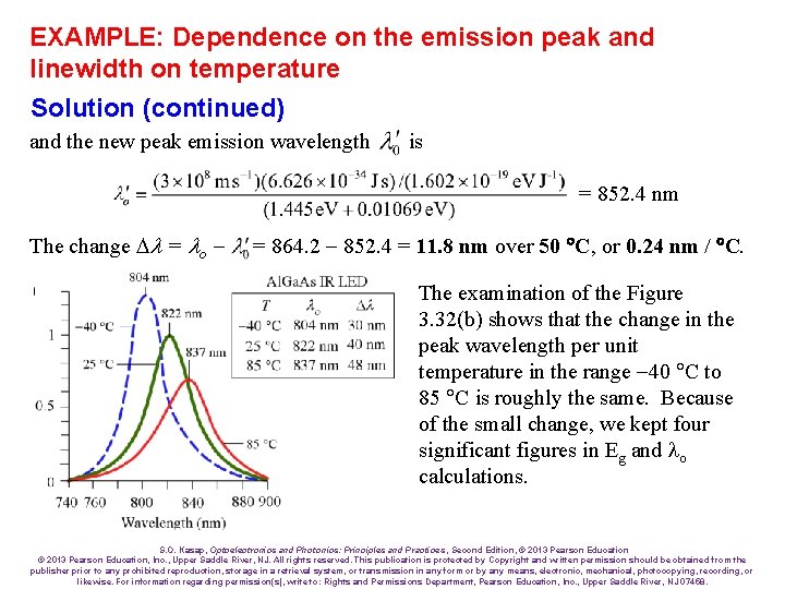
EXAMPLE: Dependence on the emission peak and linewidth on temperature Solution (continued) and the new peak emission wavelength is = 852. 4 nm The change = o - = 864. 2 - 852. 4 = 11. 8 nm over 50 C, or 0. 24 nm / C. The examination of the Figure 3. 32(b) shows that the change in the peak wavelength per unit temperature in the range -40 C to 85 C is roughly the same. Because of the small change, we kept four significant figures in Eg and lo calculations. S. O. Kasap, Optoelectronics and Photonics: Principles and Practices , Second Edition, © 2013 Pearson Education, Inc. , Upper Saddle River, NJ. All rights reserved. This publication is protected by Copyright and written permission should be obtained from the publisher prior to any prohibited reproduction, storage in a retrieval system, or transmission in any form or by any means, electronic, mechanical, photocopying, recording, or likewise. For information regarding permission(s), write to: Rights and Permissions Department, Pearson Education, Inc. , Upper Saddle River, NJ 07458.

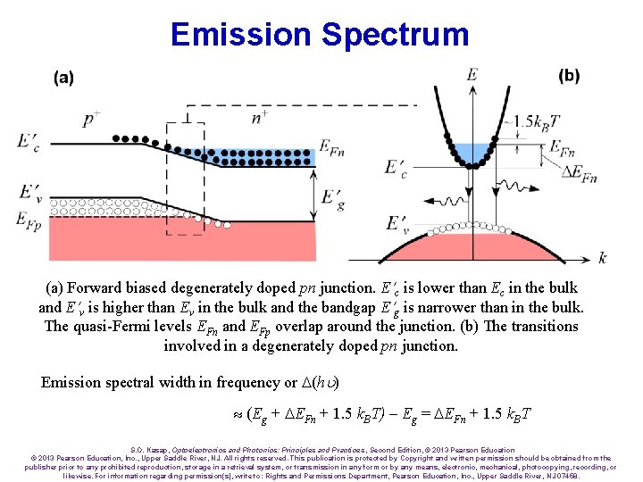
Emission Spectrum (a) Forward biased degenerately doped pn junction. E c is lower than Ec in the bulk and E v is higher than Ev in the bulk and the bandgap E g is narrower than in the bulk. The quasi-Fermi levels EFn and EFp overlap around the junction. (b) The transitions involved in a degenerately doped pn junction. Emission spectral width in frequency or (h ) (Eg + EFn + 1. 5 k. BT) - Eg = EFn + 1. 5 k. BT S. O. Kasap, Optoelectronics and Photonics: Principles and Practices , Second Edition, © 2013 Pearson Education, Inc. , Upper Saddle River, NJ. All rights reserved. This publication is protected by Copyright and written permission should be obtained from the publisher prior to any prohibited reproduction, storage in a retrieval system, or transmission in any form or by any means, electronic, mechanical, photocopying, recording, or likewise. For information regarding permission(s), write to: Rights and Permissions Department, Pearson Education, Inc. , Upper Saddle River, NJ 07458.

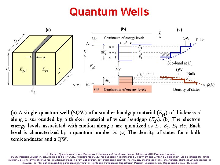
Quantum Wells (a) A single quantum well (SQW) of a smaller bandgap material (Eg 1) of thickness d along x surrounded by a thicker material of wider bandgap (Eg 2). (b) The electron energy levels associated with motion along x are quantized as E 1, E 2, E 3 etc. Each level is characterized by a quantum number n. (c) The density of states for a bulk semiconductor and a QW. S. O. Kasap, Optoelectronics and Photonics: Principles and Practices , Second Edition, © 2013 Pearson Education, Inc. , Upper Saddle River, NJ. All rights reserved. This publication is protected by Copyright and written permission should be obtained from the publisher prior to any prohibited reproduction, storage in a retrieval system, or transmission in any form or by any means, electronic, mechanical, photocopying, recording, or likewise. For information regarding permission(s), write to: Rights and Permissions Department, Pearson Education, Inc. , Upper Saddle River, NJ 07458.

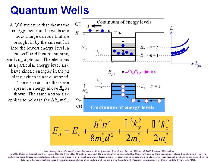
Quantum Wells A QW structure that shows the energy levels in the wells and how charge carriers that are brought in by the current fall into the lowest energy level in the well and then recombine, emitting a photon. The electrons at a particular energy level also have kinetic energies in the yz plane, which is not quantized. The electrons are therefore spread in energy above En as shown. The same notion also applies to holes in the Ev well. S. O. Kasap, Optoelectronics and Photonics: Principles and Practices , Second Edition, © 2013 Pearson Education, Inc. , Upper Saddle River, NJ. All rights reserved. This publication is protected by Copyright and written permission should be obtained from the publisher prior to any prohibited reproduction, storage in a retrieval system, or transmission in any form or by any means, electronic, mechanical, photocopying, recording, or likewise. For information regarding permission(s), write to: Rights and Permissions Department, Pearson Education, Inc. , Upper Saddle River, NJ 07458.

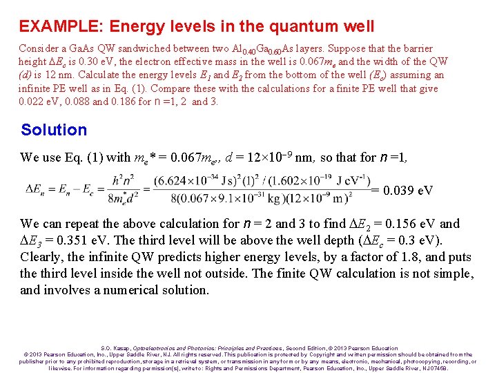
EXAMPLE: Energy levels in the quantum well Consider a Ga. As QW sandwiched between two Al 0. 40 Ga 0. 60 As layers. Suppose that the barrier height Ec is 0. 30 e. V, the electron effective mass in the well is 0. 067 me and the width of the QW (d) is 12 nm. Calculate the energy levels E 1 and E 2 from the bottom of the well (Ec) assuming an infinite PE well as in Eq. (1). Compare these with the calculations for a finite PE well that give 0. 022 e. V, 0. 088 and 0. 186 for n =1, 2 and 3. Solution We use Eq. (1) with me* = 0. 067 me, , d = 12× 10 -9 nm, so that for n =1, = 0. 039 e. V We can repeat the above calculation for n = 2 and 3 to find E 2 = 0. 156 e. V and E 3 = 0. 351 e. V. The third level will be above the well depth ( Ec = 0. 3 e. V). Clearly, the infinite QW predicts higher energy levels, by a factor of 1. 8, and puts the third level inside the well not outside. The finite QW calculation is not simple, and involves a numerical solution. S. O. Kasap, Optoelectronics and Photonics: Principles and Practices , Second Edition, © 2013 Pearson Education, Inc. , Upper Saddle River, NJ. All rights reserved. This publication is protected by Copyright and written permission should be obtained from the publisher prior to any prohibited reproduction, storage in a retrieval system, or transmission in any form or by any means, electronic, mechanical, photocopying, recording, or likewise. For information regarding permission(s), write to: Rights and Permissions Department, Pearson Education, Inc. , Upper Saddle River, NJ 07458.

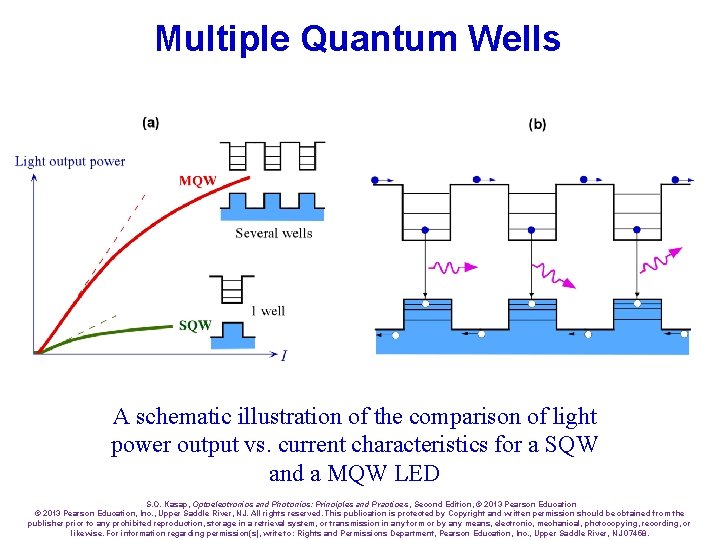
Multiple Quantum Wells A schematic illustration of the comparison of light power output vs. current characteristics for a SQW and a MQW LED S. O. Kasap, Optoelectronics and Photonics: Principles and Practices , Second Edition, © 2013 Pearson Education, Inc. , Upper Saddle River, NJ. All rights reserved. This publication is protected by Copyright and written permission should be obtained from the publisher prior to any prohibited reproduction, storage in a retrieval system, or transmission in any form or by any means, electronic, mechanical, photocopying, recording, or likewise. For information regarding permission(s), write to: Rights and Permissions Department, Pearson Education, Inc. , Upper Saddle River, NJ 07458.

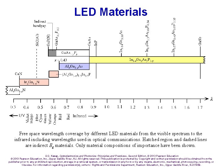
LED Materials Free space wavelength coverage by different LED materials from the visible spectrum to the infrared including wavelengths used in optical communications. Hatched region and dashed lines are indirect Eg materials. Only material compositions of importance have been shown. S. O. Kasap, Optoelectronics and Photonics: Principles and Practices , Second Edition, © 2013 Pearson Education, Inc. , Upper Saddle River, NJ. All rights reserved. This publication is protected by Copyright and written permission should be obtained from the publisher prior to any prohibited reproduction, storage in a retrieval system, or transmission in any form or by any means, electronic, mechanical, photocopying, recording, or likewise. For information regarding permission(s), write to: Rights and Permissions Department, Pearson Education, Inc. , Upper Saddle River, NJ 07458.

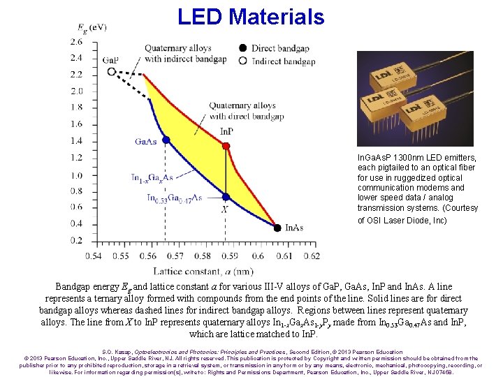
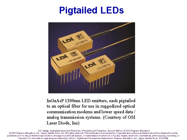
LED Materials In. Ga. As. P 1300 nm LED emitters, each pigtailed to an optical fiber for use in ruggedized optical communication modems and lower speed data / analog transmission systems. (Courtesy of OSI Laser Diode, Inc) Bandgap energy Eg and lattice constant a for various III-V alloys of Ga. P, Ga. As, In. P and In. As. A line represents a ternary alloy formed with compounds from the end points of the line. Solid lines are for direct bandgap alloys whereas dashed lines for indirect bandgap alloys. Regions between lines represent quaternary alloys. The line from X to In. P represents quaternary alloys In 1 -x. Gax. As 1 -y. Py made from In 0. 53 Ga 0. 47 As and In. P, which are lattice matched to In. P. S. O. Kasap, Optoelectronics and Photonics: Principles and Practices , Second Edition, © 2013 Pearson Education, Inc. , Upper Saddle River, NJ. All rights reserved. This publication is protected by Copyright and written permission should be obtained from the publisher prior to any prohibited reproduction, storage in a retrieval system, or transmission in any form or by any means, electronic, mechanical, photocopying, recording, or likewise. For information regarding permission(s), write to: Rights and Permissions Department, Pearson Education, Inc. , Upper Saddle River, NJ 07458.

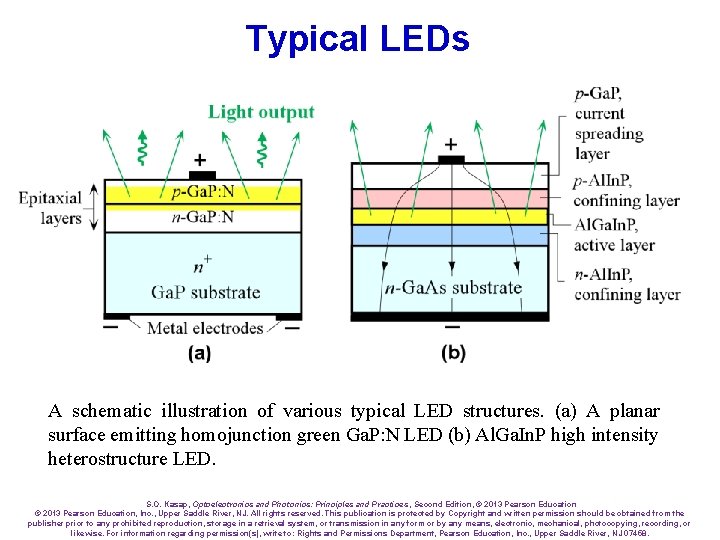
Typical LEDs A schematic illustration of various typical LED structures. (a) A planar surface emitting homojunction green Ga. P: N LED (b) Al. Ga. In. P high intensity heterostructure LED. S. O. Kasap, Optoelectronics and Photonics: Principles and Practices , Second Edition, © 2013 Pearson Education, Inc. , Upper Saddle River, NJ. All rights reserved. This publication is protected by Copyright and written permission should be obtained from the publisher prior to any prohibited reproduction, storage in a retrieval system, or transmission in any form or by any means, electronic, mechanical, photocopying, recording, or likewise. For information regarding permission(s), write to: Rights and Permissions Department, Pearson Education, Inc. , Upper Saddle River, NJ 07458.

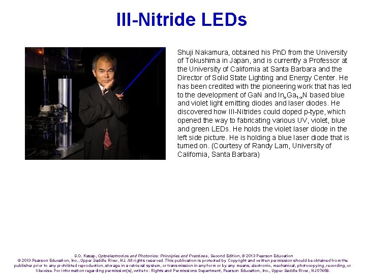
III-Nitride LEDs Shuji Nakamura, obtained his Ph. D from the University of Tokushima in Japan, and is currently a Professor at the University of California at Santa Barbara and the Director of Solid State Lighting and Energy Center. He has been credited with the pioneering work that has led to the development of Ga. N and Inx. Ga 1 -x. N based blue and violet light emitting diodes and laser diodes. He discovered how III-Nitrides could doped p-type, which opened the way to fabricating various UV, violet, blue and green LEDs. He holds the violet laser diode in the left side picture. He is holding a blue laser diode that is turned on. (Courtesy of Randy Lam, University of California, Santa Barbara) S. O. Kasap, Optoelectronics and Photonics: Principles and Practices , Second Edition, © 2013 Pearson Education, Inc. , Upper Saddle River, NJ. All rights reserved. This publication is protected by Copyright and written permission should be obtained from the publisher prior to any prohibited reproduction, storage in a retrieval system, or transmission in any form or by any means, electronic, mechanical, photocopying, recording, or likewise. For information regarding permission(s), write to: Rights and Permissions Department, Pearson Education, Inc. , Upper Saddle River, NJ 07458.

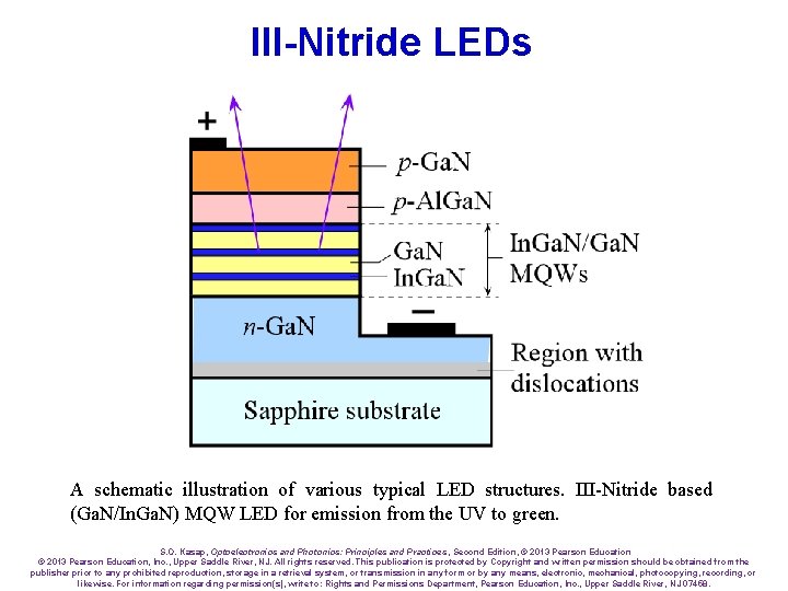
III-Nitride LEDs A schematic illustration of various typical LED structures. III-Nitride based (Ga. N/In. Ga. N) MQW LED for emission from the UV to green. S. O. Kasap, Optoelectronics and Photonics: Principles and Practices , Second Edition, © 2013 Pearson Education, Inc. , Upper Saddle River, NJ. All rights reserved. This publication is protected by Copyright and written permission should be obtained from the publisher prior to any prohibited reproduction, storage in a retrieval system, or transmission in any form or by any means, electronic, mechanical, photocopying, recording, or likewise. For information regarding permission(s), write to: Rights and Permissions Department, Pearson Education, Inc. , Upper Saddle River, NJ 07458.

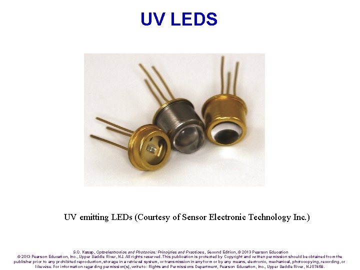
UV LEDS UV emitting LEDs (Courtesy of Sensor Electronic Technology Inc. ) S. O. Kasap, Optoelectronics and Photonics: Principles and Practices , Second Edition, © 2013 Pearson Education, Inc. , Upper Saddle River, NJ. All rights reserved. This publication is protected by Copyright and written permission should be obtained from the publisher prior to any prohibited reproduction, storage in a retrieval system, or transmission in any form or by any means, electronic, mechanical, photocopying, recording, or likewise. For information regarding permission(s), write to: Rights and Permissions Department, Pearson Education, Inc. , Upper Saddle River, NJ 07458.

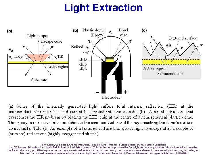
Light Extraction (a) Some of the internally generated light suffers total internal reflection (TIR) at the semiconductor/air interface and cannot be emitted into the outside. (b) A simple structure that overcomes the TIR problem by placing the LED chip at the centre of a hemispherical plastic dome. The epoxy is refractive index matched to the semiconductor and the rays reaching the dome's surface do not suffer TIR. (b) An example of a textured surface that allows light to escape after a couple of (or more) reflections (highly exaggerated sketch). S. O. Kasap, Optoelectronics and Photonics: Principles and Practices , Second Edition, © 2013 Pearson Education, Inc. , Upper Saddle River, NJ. All rights reserved. This publication is protected by Copyright and written permission should be obtained from the publisher prior to any prohibited reproduction, storage in a retrieval system, or transmission in any form or by any means, electronic, mechanical, photocopying, recording, or likewise. For information regarding permission(s), write to: Rights and Permissions Department, Pearson Education, Inc. , Upper Saddle River, NJ 07458.

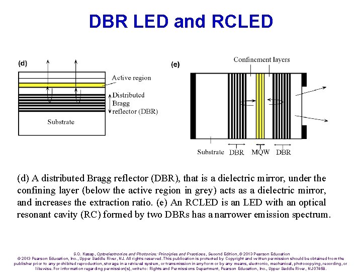
DBR LED and RCLED (d) A distributed Bragg reflector (DBR), that is a dielectric mirror, under the confining layer (below the active region in grey) acts as a dielectric mirror, and increases the extraction ratio. (e) An RCLED is an LED with an optical resonant cavity (RC) formed by two DBRs has a narrower emission spectrum. S. O. Kasap, Optoelectronics and Photonics: Principles and Practices , Second Edition, © 2013 Pearson Education, Inc. , Upper Saddle River, NJ. All rights reserved. This publication is protected by Copyright and written permission should be obtained from the publisher prior to any prohibited reproduction, storage in a retrieval system, or transmission in any form or by any means, electronic, mechanical, photocopying, recording, or likewise. For information regarding permission(s), write to: Rights and Permissions Department, Pearson Education, Inc. , Upper Saddle River, NJ 07458.

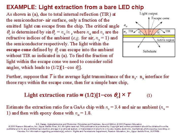
EXAMPLE: Light extraction from a bare LED chip As shown in (a), due to total internal reflection (TIR) at the semiconductor- air surface, only a fraction of the emitted light can escape from the chip. The critical angle qc is determined by sinqc = na /n s where na and ns are the refractive indices of the ambient (e. g. for air, na = 1) and the semiconductor respectively. The light within the escape cone defined by qc can escape into the ambient without TIR as indicated in (a). To find the fraction of light within the escape cone we need to consider solid angles, which leads to (1/2)[1 -cos qc]. Further, suppose that T is the average light transmittance of the ns- na interface for those rays within the escape cone, then for a simple bare chip, Light extraction ratio (1/2)[1 -cos qc] × T (1) Estimate the extraction ratio for a Ga. As chip with ns = 3. 4 and air as ambient (na = 1) and then with epoxy dome with na = 1. 8. S. O. Kasap, Optoelectronics and Photonics: Principles and Practices , Second Edition, © 2013 Pearson Education, Inc. , Upper Saddle River, NJ. All rights reserved. This publication is protected by Copyright and written permission should be obtained from the publisher prior to any prohibited reproduction, storage in a retrieval system, or transmission in any form or by any means, electronic, mechanical, photocopying, recording, or likewise. For information regarding permission(s), write to: Rights and Permissions Department, Pearson Education, Inc. , Upper Saddle River, NJ 07458.

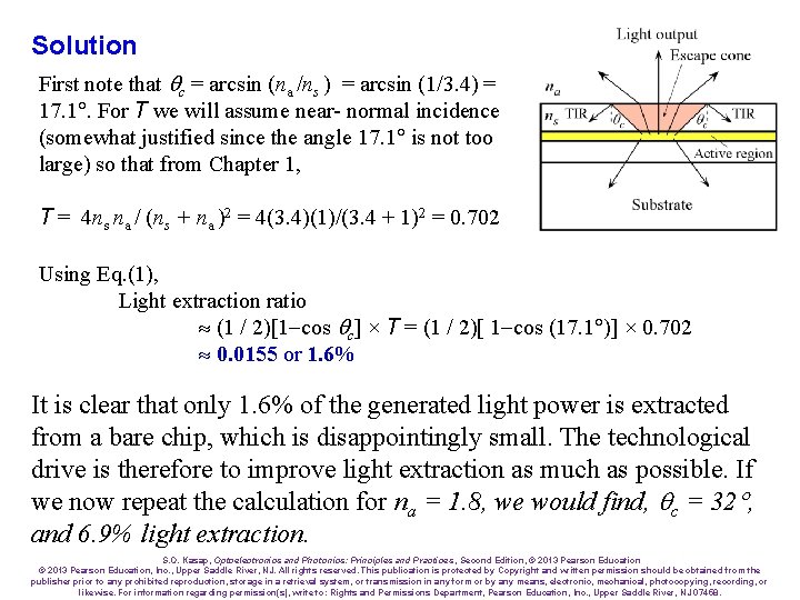
Solution First note that qc = arcsin (na /ns ) = arcsin (1/3. 4) = 17. 1. For T we will assume near- normal incidence (somewhat justified since the angle 17. 1 is not too large) so that from Chapter 1, T = 4 ns na / (ns + na )2 = 4(3. 4)(1)/(3. 4 + 1)2 = 0. 702 Using Eq. (1), Light extraction ratio (1 / 2)[1 -cos qc] × T = (1 / 2)[ 1 -cos (17. 1 )] × 0. 702 0. 0155 or 1. 6% It is clear that only 1. 6% of the generated light power is extracted from a bare chip, which is disappointingly small. The technological drive is therefore to improve light extraction as much as possible. If we now repeat the calculation for na = 1. 8, we would find, qc = 32 , and 6. 9% light extraction. S. O. Kasap, Optoelectronics and Photonics: Principles and Practices , Second Edition, © 2013 Pearson Education, Inc. , Upper Saddle River, NJ. All rights reserved. This publication is protected by Copyright and written permission should be obtained from the publisher prior to any prohibited reproduction, storage in a retrieval system, or transmission in any form or by any means, electronic, mechanical, photocopying, recording, or likewise. For information regarding permission(s), write to: Rights and Permissions Department, Pearson Education, Inc. , Upper Saddle River, NJ 07458.

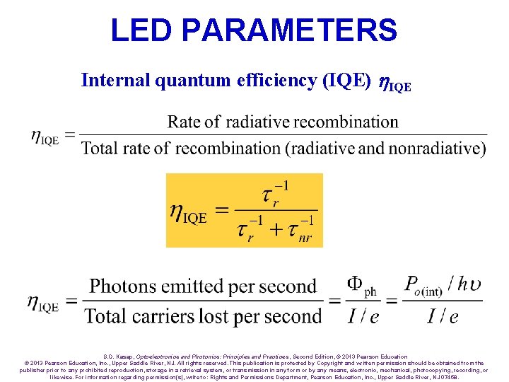
LED PARAMETERS Internal quantum efficiency (IQE) h. IQE S. O. Kasap, Optoelectronics and Photonics: Principles and Practices , Second Edition, © 2013 Pearson Education, Inc. , Upper Saddle River, NJ. All rights reserved. This publication is protected by Copyright and written permission should be obtained from the publisher prior to any prohibited reproduction, storage in a retrieval system, or transmission in any form or by any means, electronic, mechanical, photocopying, recording, or likewise. For information regarding permission(s), write to: Rights and Permissions Department, Pearson Education, Inc. , Upper Saddle River, NJ 07458.

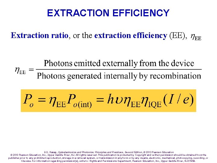
EXTRACTION EFFICIENCY Extraction ratio, or the extraction efficiency (EE), h. EE S. O. Kasap, Optoelectronics and Photonics: Principles and Practices , Second Edition, © 2013 Pearson Education, Inc. , Upper Saddle River, NJ. All rights reserved. This publication is protected by Copyright and written permission should be obtained from the publisher prior to any prohibited reproduction, storage in a retrieval system, or transmission in any form or by any means, electronic, mechanical, photocopying, recording, or likewise. For information regarding permission(s), write to: Rights and Permissions Department, Pearson Education, Inc. , Upper Saddle River, NJ 07458.

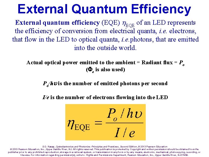
External Quantum Efficiency External quantum efficiency (EQE) h. EQE of an LED represents the efficiency of conversion from electrical quanta, i. e. electrons, that flow in the LED to optical quanta, i. e. photons, that are emitted into the outside world. Actual optical power emitted to the ambient = Radiant flux = Po (Fe is also used) Po/hu is the number of emitted photons per second I/e is the number of electrons flowing into the LED S. O. Kasap, Optoelectronics and Photonics: Principles and Practices , Second Edition, © 2013 Pearson Education, Inc. , Upper Saddle River, NJ. All rights reserved. This publication is protected by Copyright and written permission should be obtained from the publisher prior to any prohibited reproduction, storage in a retrieval system, or transmission in any form or by any means, electronic, mechanical, photocopying, recording, or likewise. For information regarding permission(s), write to: Rights and Permissions Department, Pearson Education, Inc. , Upper Saddle River, NJ 07458.

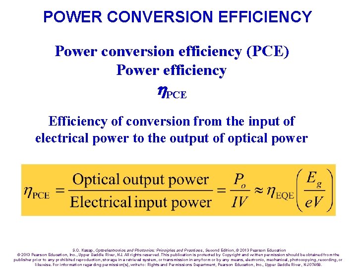
POWER CONVERSION EFFICIENCY Power conversion efficiency (PCE) Power efficiency h. PCE Efficiency of conversion from the input of electrical power to the output of optical power S. O. Kasap, Optoelectronics and Photonics: Principles and Practices , Second Edition, © 2013 Pearson Education, Inc. , Upper Saddle River, NJ. All rights reserved. This publication is protected by Copyright and written permission should be obtained from the publisher prior to any prohibited reproduction, storage in a retrieval system, or transmission in any form or by any means, electronic, mechanical, photocopying, recording, or likewise. For information regarding permission(s), write to: Rights and Permissions Department, Pearson Education, Inc. , Upper Saddle River, NJ 07458.

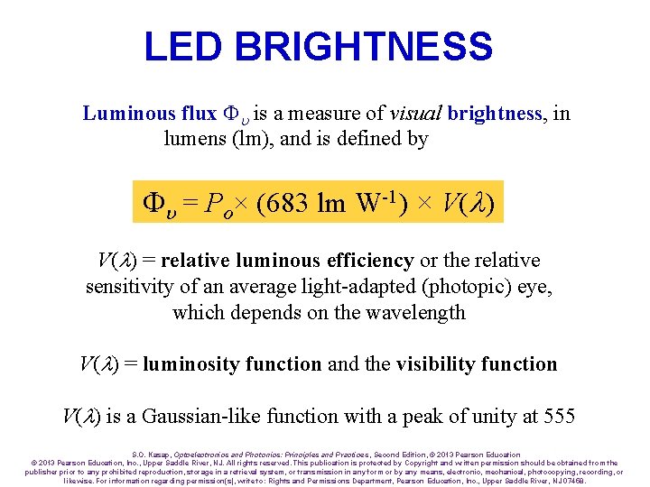
LED BRIGHTNESS Luminous flux is a measure of visual brightness, in lumens (lm), and is defined by = Po× (683 lm W-1) × V( ) = relative luminous efficiency or the relative sensitivity of an average light-adapted (photopic) eye, which depends on the wavelength V( ) = luminosity function and the visibility function V( ) is a Gaussian-like function with a peak of unity at 555 S. O. Kasap, Optoelectronics and Photonics: Principles and Practices , Second Edition, © 2013 Pearson Education, Inc. , Upper Saddle River, NJ. All rights reserved. This publication is protected by Copyright and written permission should be obtained from the publisher prior to any prohibited reproduction, storage in a retrieval system, or transmission in any form or by any means, electronic, mechanical, photocopying, recording, or likewise. For information regarding permission(s), write to: Rights and Permissions Department, Pearson Education, Inc. , Upper Saddle River, NJ 07458.

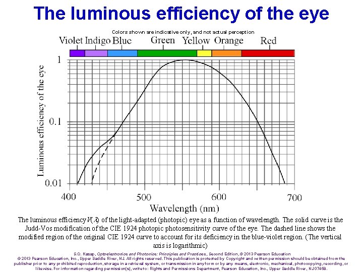
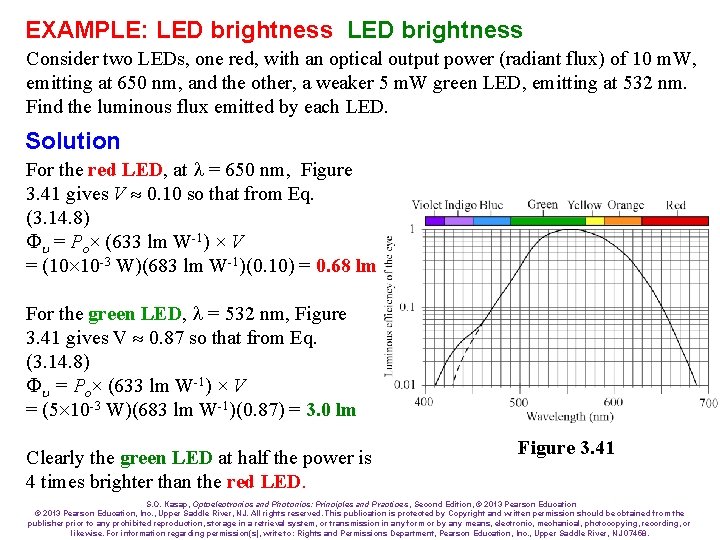
The luminous efficiency of the eye Colors shown are indicative only, and not actual perception The luminous efficiency. V( ) of the light-adapted (photopic) eye as a function of wavelength. The solid curve is the Judd-Vos modification of the CIE 1924 photopic photosensitivity curve of the eye. The dashed line shows the modified region of the original CIE 1924 curve to account for its deficiency in the blue-violet region. (The vertical axis is logarithmic) S. O. Kasap, Optoelectronics and Photonics: Principles and Practices , Second Edition, © 2013 Pearson Education, Inc. , Upper Saddle River, NJ. All rights reserved. This publication is protected by Copyright and written permission should be obtained from the publisher prior to any prohibited reproduction, storage in a retrieval system, or transmission in any form or by any means, electronic, mechanical, photocopying, recording, or likewise. For information regarding permission(s), write to: Rights and Permissions Department, Pearson Education, Inc. , Upper Saddle River, NJ 07458.

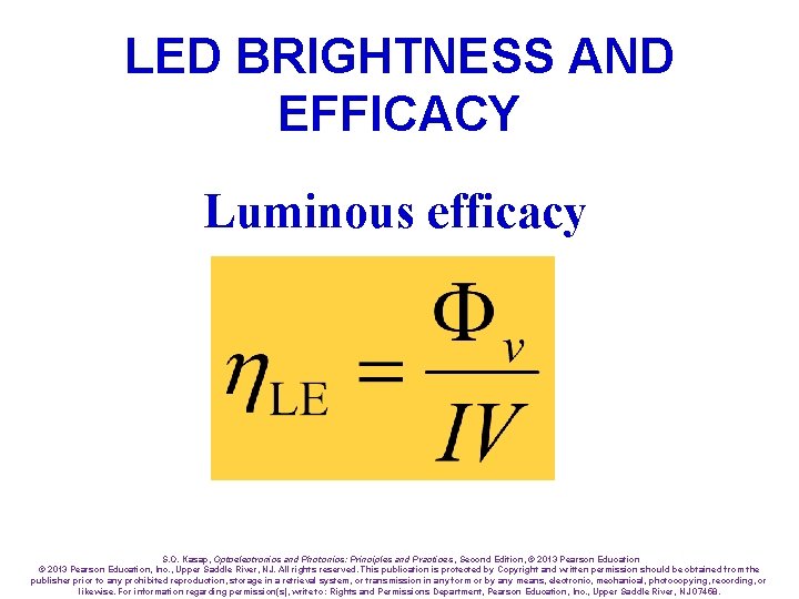
LED BRIGHTNESS AND EFFICACY Luminous efficacy S. O. Kasap, Optoelectronics and Photonics: Principles and Practices , Second Edition, © 2013 Pearson Education, Inc. , Upper Saddle River, NJ. All rights reserved. This publication is protected by Copyright and written permission should be obtained from the publisher prior to any prohibited reproduction, storage in a retrieval system, or transmission in any form or by any means, electronic, mechanical, photocopying, recording, or likewise. For information regarding permission(s), write to: Rights and Permissions Department, Pearson Education, Inc. , Upper Saddle River, NJ 07458.

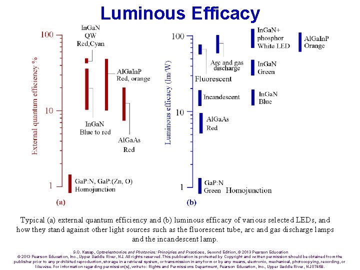
Luminous Efficacy Typical (a) external quantum efficiency and (b) luminous efficacy of various selected LEDs, and how they stand against other light sources such as the fluorescent tube, arc and gas discharge lamps and the incandescent lamp. S. O. Kasap, Optoelectronics and Photonics: Principles and Practices , Second Edition, © 2013 Pearson Education, Inc. , Upper Saddle River, NJ. All rights reserved. This publication is protected by Copyright and written permission should be obtained from the publisher prior to any prohibited reproduction, storage in a retrieval system, or transmission in any form or by any means, electronic, mechanical, photocopying, recording, or likewise. For information regarding permission(s), write to: Rights and Permissions Department, Pearson Education, Inc. , Upper Saddle River, NJ 07458.

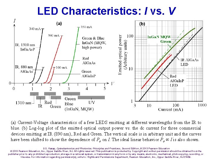
LED Characteristics: I vs. V (a) Current-Voltage characteristics of a few LEDS emitting at different wavelengths from the IR to blue. (b) Log-log plot of the emitted optical output power vs. the dc current for three commercial devices emitting at IR (890 nm), Red and Green. The vertical scale is in arbitrary unit and the curves have been shifted to show the dependence of Po on I. The ideal linear behavior Po I is also shown. S. O. Kasap, Optoelectronics and Photonics: Principles and Practices , Second Edition, © 2013 Pearson Education, Inc. , Upper Saddle River, NJ. All rights reserved. This publication is protected by Copyright and written permission should be obtained from the publisher prior to any prohibited reproduction, storage in a retrieval system, or transmission in any form or by any means, electronic, mechanical, photocopying, recording, or likewise. For information regarding permission(s), write to: Rights and Permissions Department, Pearson Education, Inc. , Upper Saddle River, NJ 07458.

EXAMPLE: LED brightness Consider two LEDs, one red, with an optical output power (radiant flux) of 10 m. W, emitting at 650 nm, and the other, a weaker 5 m. W green LED, emitting at 532 nm. Find the luminous flux emitted by each LED. Solution For the red LED, at l = 650 nm, Figure 3. 41 gives V 0. 10 so that from Eq. (3. 14. 8) = Po× (633 lm W-1) × V = (10 10 -3 W)(683 lm W-1)(0. 10) = 0. 68 lm For the green LED, l = 532 nm, Figure 3. 41 gives V 0. 87 so that from Eq. (3. 14. 8) = Po× (633 lm W-1) × V = (5 10 -3 W)(683 lm W-1)(0. 87) = 3. 0 lm Clearly the green LED at half the power is 4 times brighter than the red LED. Figure 3. 41 S. O. Kasap, Optoelectronics and Photonics: Principles and Practices , Second Edition, © 2013 Pearson Education, Inc. , Upper Saddle River, NJ. All rights reserved. This publication is protected by Copyright and written permission should be obtained from the publisher prior to any prohibited reproduction, storage in a retrieval system, or transmission in any form or by any means, electronic, mechanical, photocopying, recording, or likewise. For information regarding permission(s), write to: Rights and Permissions Department, Pearson Education, Inc. , Upper Saddle River, NJ 07458.

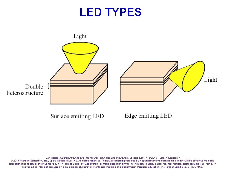
LED TYPES S. O. Kasap, Optoelectronics and Photonics: Principles and Practices , Second Edition, © 2013 Pearson Education, Inc. , Upper Saddle River, NJ. All rights reserved. This publication is protected by Copyright and written permission should be obtained from the publisher prior to any prohibited reproduction, storage in a retrieval system, or transmission in any form or by any means, electronic, mechanical, photocopying, recording, or likewise. For information regarding permission(s), write to: Rights and Permissions Department, Pearson Education, Inc. , Upper Saddle River, NJ 07458.

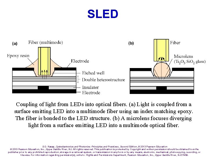
SLED Coupling of light from LEDs into optical fibers. (a) Light is coupled from a surface emitting LED into a multimode fiber using an index matching epoxy. The fiber is bonded to the LED structure. (b) A microlens focuses diverging light from a surface emitting LED into a multimode optical fiber. S. O. Kasap, Optoelectronics and Photonics: Principles and Practices , Second Edition, © 2013 Pearson Education, Inc. , Upper Saddle River, NJ. All rights reserved. This publication is protected by Copyright and written permission should be obtained from the publisher prior to any prohibited reproduction, storage in a retrieval system, or transmission in any form or by any means, electronic, mechanical, photocopying, recording, or likewise. For information regarding permission(s), write to: Rights and Permissions Department, Pearson Education, Inc. , Upper Saddle River, NJ 07458.

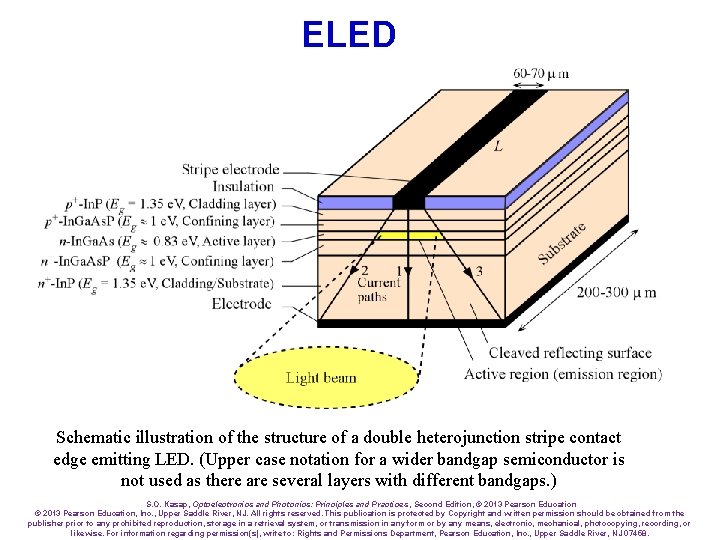
ELED Schematic illustration of the structure of a double heterojunction stripe contact edge emitting LED. (Upper case notation for a wider bandgap semiconductor is not used as there are several layers with different bandgaps. ) S. O. Kasap, Optoelectronics and Photonics: Principles and Practices , Second Edition, © 2013 Pearson Education, Inc. , Upper Saddle River, NJ. All rights reserved. This publication is protected by Copyright and written permission should be obtained from the publisher prior to any prohibited reproduction, storage in a retrieval system, or transmission in any form or by any means, electronic, mechanical, photocopying, recording, or likewise. For information regarding permission(s), write to: Rights and Permissions Department, Pearson Education, Inc. , Upper Saddle River, NJ 07458.

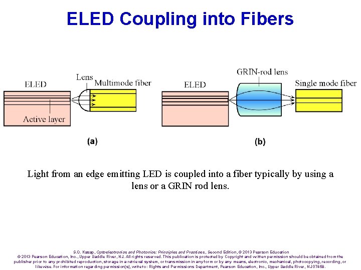
ELED Coupling into Fibers Light from an edge emitting LED is coupled into a fiber typically by using a lens or a GRIN rod lens. S. O. Kasap, Optoelectronics and Photonics: Principles and Practices , Second Edition, © 2013 Pearson Education, Inc. , Upper Saddle River, NJ. All rights reserved. This publication is protected by Copyright and written permission should be obtained from the publisher prior to any prohibited reproduction, storage in a retrieval system, or transmission in any form or by any means, electronic, mechanical, photocopying, recording, or likewise. For information regarding permission(s), write to: Rights and Permissions Department, Pearson Education, Inc. , Upper Saddle River, NJ 07458.

Pigtailed LEDs In. Ga. As. P 1300 nm LED emitters, each pigtailed to an optical fiber for use in ruggedized optical communication modems and lower speed data / analog transmission systems. (Courtesy of OSI Laser Diode, Inc) S. O. Kasap, Optoelectronics and Photonics: Principles and Practices , Second Edition, © 2013 Pearson Education, Inc. , Upper Saddle River, NJ. All rights reserved. This publication is protected by Copyright and written permission should be obtained from the publisher prior to any prohibited reproduction, storage in a retrieval system, or transmission in any form or by any means, electronic, mechanical, photocopying, recording, or likewise. For information regarding permission(s), write to: Rights and Permissions Department, Pearson Education, Inc. , Upper Saddle River, NJ 07458.

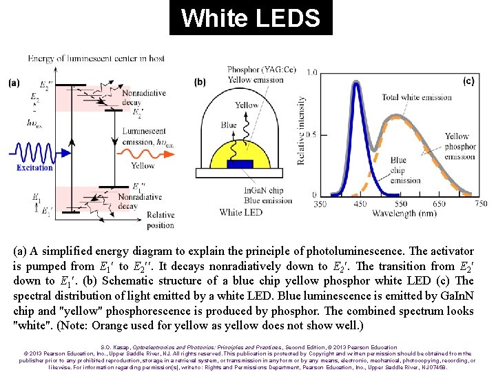
White LEDS (a) A simplified energy diagram to explain the principle of photoluminescence. The activator is pumped from E 1 to E 2 . It decays nonradiatively down to E 2. The transition from E 2 down to E 1. (b) Schematic structure of a blue chip yellow phosphor white LED (c) The spectral distribution of light emitted by a white LED. Blue luminescence is emitted by Ga. In. N chip and "yellow" phosphorescence is produced by phosphor. The combined spectrum looks "white". (Note: Orange used for yellow as yellow does not show well. ) S. O. Kasap, Optoelectronics and Photonics: Principles and Practices , Second Edition, © 2013 Pearson Education, Inc. , Upper Saddle River, NJ. All rights reserved. This publication is protected by Copyright and written permission should be obtained from the publisher prior to any prohibited reproduction, storage in a retrieval system, or transmission in any form or by any means, electronic, mechanical, photocopying, recording, or likewise. For information regarding permission(s), write to: Rights and Permissions Department, Pearson Education, Inc. , Upper Saddle River, NJ 07458.

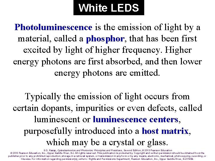
White LEDS Photoluminescence is the emission of light by a material, called a phosphor, that has been first excited by light of higher frequency. Higher energy photons are first absorbed, and then lower energy photons are emitted. Typically the emission of light occurs from certain dopants, impurities or even defects, called luminescent or luminescence centers, purposefully introduced into a host matrix, which may be a crystal or glass. S. O. Kasap, Optoelectronics and Photonics: Principles and Practices , Second Edition, © 2013 Pearson Education, Inc. , Upper Saddle River, NJ. All rights reserved. This publication is protected by Copyright and written permission should be obtained from the publisher prior to any prohibited reproduction, storage in a retrieval system, or transmission in any form or by any means, electronic, mechanical, photocopying, recording, or likewise. For information regarding permission(s), write to: Rights and Permissions Department, Pearson Education, Inc. , Upper Saddle River, NJ 07458.

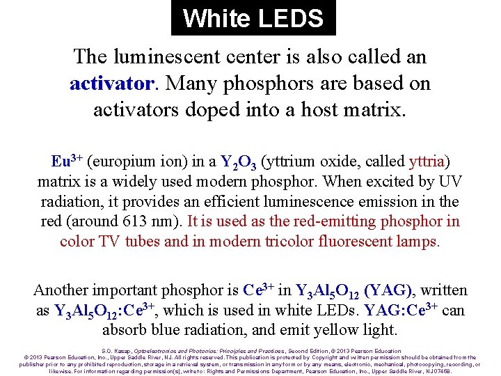
White LEDS The luminescenter is also called an activator. Many phosphors are based on activators doped into a host matrix. Eu 3+ (europium ion) in a Y 2 O 3 (yttrium oxide, called yttria) matrix is a widely used modern phosphor. When excited by UV radiation, it provides an efficient luminescence emission in the red (around 613 nm). It is used as the red-emitting phosphor in color TV tubes and in modern tricolor fluorescent lamps. Another important phosphor is Ce 3+ in Y 3 Al 5 O 12 (YAG), written as Y 3 Al 5 O 12: Ce 3+, which is used in white LEDs. YAG: Ce 3+ can absorb blue radiation, and emit yellow light. S. O. Kasap, Optoelectronics and Photonics: Principles and Practices , Second Edition, © 2013 Pearson Education, Inc. , Upper Saddle River, NJ. All rights reserved. This publication is protected by Copyright and written permission should be obtained from the publisher prior to any prohibited reproduction, storage in a retrieval system, or transmission in any form or by any means, electronic, mechanical, photocopying, recording, or likewise. For information regarding permission(s), write to: Rights and Permissions Department, Pearson Education, Inc. , Upper Saddle River, NJ 07458.

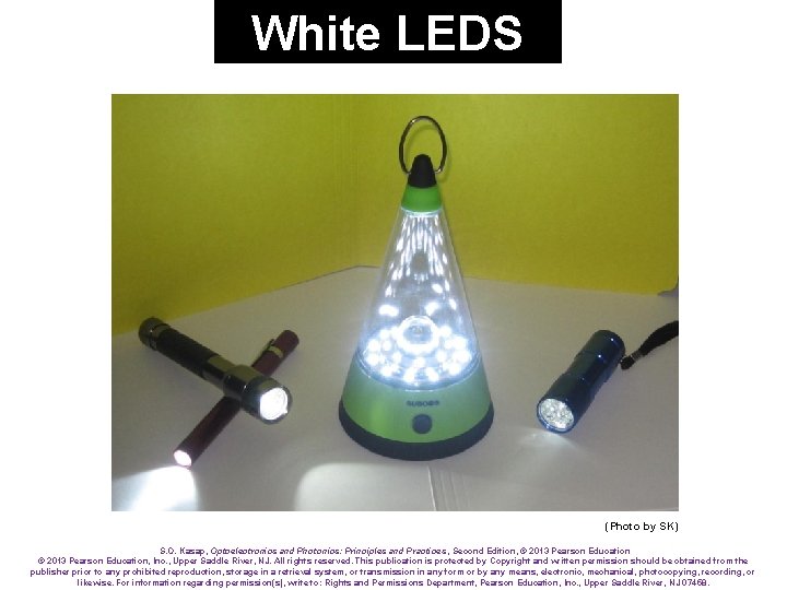
White LEDS (Photo by SK) S. O. Kasap, Optoelectronics and Photonics: Principles and Practices , Second Edition, © 2013 Pearson Education, Inc. , Upper Saddle River, NJ. All rights reserved. This publication is protected by Copyright and written permission should be obtained from the publisher prior to any prohibited reproduction, storage in a retrieval system, or transmission in any form or by any means, electronic, mechanical, photocopying, recording, or likewise. For information regarding permission(s), write to: Rights and Permissions Department, Pearson Education, Inc. , Upper Saddle River, NJ 07458.

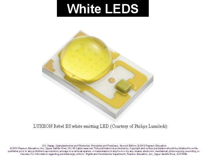
White LEDS LUXEON Rebel ES white emitting LED (Courtesy of Philips Lumileds) S. O. Kasap, Optoelectronics and Photonics: Principles and Practices , Second Edition, © 2013 Pearson Education, Inc. , Upper Saddle River, NJ. All rights reserved. This publication is protected by Copyright and written permission should be obtained from the publisher prior to any prohibited reproduction, storage in a retrieval system, or transmission in any form or by any means, electronic, mechanical, photocopying, recording, or likewise. For information regarding permission(s), write to: Rights and Permissions Department, Pearson Education, Inc. , Upper Saddle River, NJ 07458.

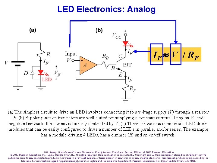
LED Electronics: Analog IF V / RF (a) The simplest circuit to drive an LED involves connecting it to a voltage supply (V) through a resistor R. (b) Bipolar junction transistors are well suited for supplying a constant current. Using an IC and negative feedback, the current is linearly controlled by V. (c) There are various commercial LED driver modules that can be easily configured to drive a number of LEDs in parallel and/or series. The example has a module driving 4 LEDs, has a dimmer (R) and an on/off switch. S. O. Kasap, Optoelectronics and Photonics: Principles and Practices , Second Edition, © 2013 Pearson Education, Inc. , Upper Saddle River, NJ. All rights reserved. This publication is protected by Copyright and written permission should be obtained from the publisher prior to any prohibited reproduction, storage in a retrieval system, or transmission in any form or by any means, electronic, mechanical, photocopying, recording, or likewise. For information regarding permission(s), write to: Rights and Permissions Department, Pearson Education, Inc. , Upper Saddle River, NJ 07458.

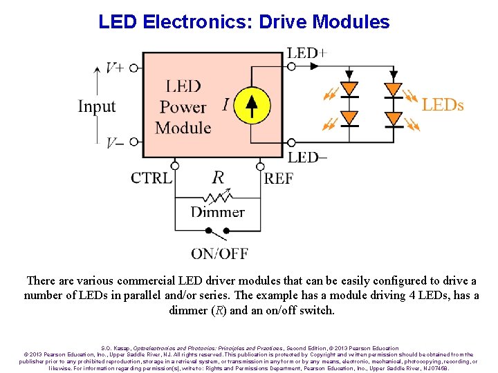
LED Electronics: Drive Modules There are various commercial LED driver modules that can be easily configured to drive a number of LEDs in parallel and/or series. The example has a module driving 4 LEDs, has a dimmer (R) and an on/off switch. S. O. Kasap, Optoelectronics and Photonics: Principles and Practices , Second Edition, © 2013 Pearson Education, Inc. , Upper Saddle River, NJ. All rights reserved. This publication is protected by Copyright and written permission should be obtained from the publisher prior to any prohibited reproduction, storage in a retrieval system, or transmission in any form or by any means, electronic, mechanical, photocopying, recording, or likewise. For information regarding permission(s), write to: Rights and Permissions Department, Pearson Education, Inc. , Upper Saddle River, NJ 07458.

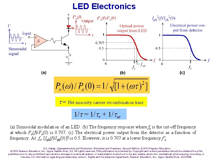
LED Electronics t = Net minority carrier recombination time 1/t = 1/tr + 1/tnr (a) Sinusoidal modulation of an LED. (b) The frequency response where fc is the cut-off frequency at which Po(f)/Po(0) is 0. 707. (c) The electrical power output from the detector as a function of frequency. At fc, [Iph(f)/Iph(0)]2 is 0. 5. However, it is 0. 707 at a lower frequency f c. S. O. Kasap, Optoelectronics and Photonics: Principles and Practices , Second Edition, © 2013 Pearson Education, Inc. , Upper Saddle River, NJ. All rights reserved. This publication is protected by Copyright and written permission should be obtained from the publisher prior to any prohibited reproduction, storage in a retrieval system, or transmission in any form or by any means, electronic, mechanical, photocopying, recording, or likewise. For information regarding permission(s), write to: Rights and Permissions Department, Pearson Education, Inc. , Upper Saddle River, NJ 07458.

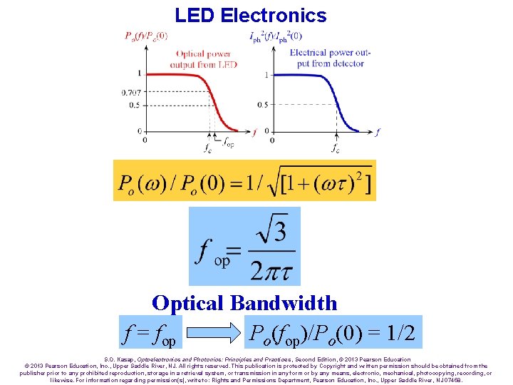
LED Electronics Optical Bandwidth f = fop Po(fop)/Po(0) = 1/2 S. O. Kasap, Optoelectronics and Photonics: Principles and Practices , Second Edition, © 2013 Pearson Education, Inc. , Upper Saddle River, NJ. All rights reserved. This publication is protected by Copyright and written permission should be obtained from the publisher prior to any prohibited reproduction, storage in a retrieval system, or transmission in any form or by any means, electronic, mechanical, photocopying, recording, or likewise. For information regarding permission(s), write to: Rights and Permissions Department, Pearson Education, Inc. , Upper Saddle River, NJ 07458.

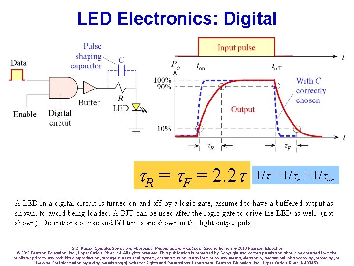
LED Electronics: Digital t. R = t. F = 2. 2 t 1/t = 1/tr + 1/tnr A LED in a digital circuit is turned on and off by a logic gate, assumed to have a buffered output as shown, to avoid being loaded. A BJT can be used after the logic gate to drive the LED as well (not shown). Definitions of rise and fall times are shown in the light output pulse. S. O. Kasap, Optoelectronics and Photonics: Principles and Practices , Second Edition, © 2013 Pearson Education, Inc. , Upper Saddle River, NJ. All rights reserved. This publication is protected by Copyright and written permission should be obtained from the publisher prior to any prohibited reproduction, storage in a retrieval system, or transmission in any form or by any means, electronic, mechanical, photocopying, recording, or likewise. For information regarding permission(s), write to: Rights and Permissions Department, Pearson Education, Inc. , Upper Saddle River, NJ 07458.

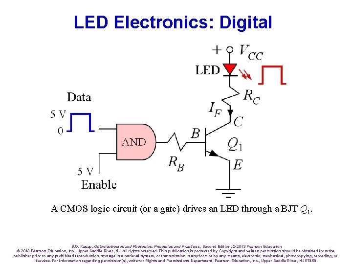
LED Electronics: Digital A CMOS logic circuit (or a gate) drives an LED through a BJT Q 1. S. O. Kasap, Optoelectronics and Photonics: Principles and Practices , Second Edition, © 2013 Pearson Education, Inc. , Upper Saddle River, NJ. All rights reserved. This publication is protected by Copyright and written permission should be obtained from the publisher prior to any prohibited reproduction, storage in a retrieval system, or transmission in any form or by any means, electronic, mechanical, photocopying, recording, or likewise. For information regarding permission(s), write to: Rights and Permissions Department, Pearson Education, Inc. , Upper Saddle River, NJ 07458.

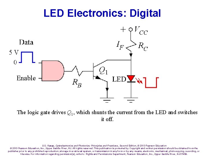
LED Electronics: Digital Enable The logic gate drives Q 1, which shunts the current from the LED and switches it off. S. O. Kasap, Optoelectronics and Photonics: Principles and Practices , Second Edition, © 2013 Pearson Education, Inc. , Upper Saddle River, NJ. All rights reserved. This publication is protected by Copyright and written permission should be obtained from the publisher prior to any prohibited reproduction, storage in a retrieval system, or transmission in any form or by any means, electronic, mechanical, photocopying, recording, or likewise. For information regarding permission(s), write to: Rights and Permissions Department, Pearson Education, Inc. , Upper Saddle River, NJ 07458.

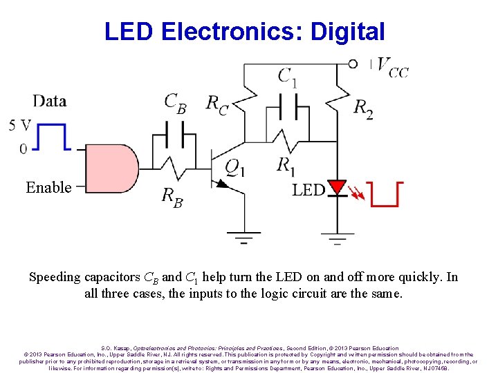
LED Electronics: Digital Enable Speeding capacitors CB and C 1 help turn the LED on and off more quickly. In all three cases, the inputs to the logic circuit are the same. S. O. Kasap, Optoelectronics and Photonics: Principles and Practices , Second Edition, © 2013 Pearson Education, Inc. , Upper Saddle River, NJ. All rights reserved. This publication is protected by Copyright and written permission should be obtained from the publisher prior to any prohibited reproduction, storage in a retrieval system, or transmission in any form or by any means, electronic, mechanical, photocopying, recording, or likewise. For information regarding permission(s), write to: Rights and Permissions Department, Pearson Education, Inc. , Upper Saddle River, NJ 07458.

Updates and Corrected Slides Class Demonstrations Class Problems Check author’s website http: //optoelectronics. usask. ca Email errors and corrections to safa. kasap@yahoo. com S. O. Kasap, Optoelectronics and Photonics: Principles and Practices , Second Edition, © 2013 Pearson Education, Inc. , Upper Saddle River, NJ. All rights reserved. This publication is protected by Copyright and written permission should be obtained from the publisher prior to any prohibited reproduction, storage in a retrieval system, or transmission in any form or by any means, electronic, mechanical, photocopying, recording, or likewise. For information regarding permission(s), write to: Rights and Permissions Department, Pearson Education, Inc. , Upper Saddle River, NJ 07458.