Examen cours Cristaux Photoniques Mechanical tuning of Photonic
- Slides: 16

Examen cours Cristaux Photoniques Mechanical tuning of Photonic Crystals July 23, 2009 Fabio Jutzi Ph. D student EDMI Ecole Polytechnique Fédérale de Lausanne Sensors, Actuators and Microsystems Laboratory EPFL STI IMT SAMLAB Rue Jaquet Droz 1 CH-2002 Neuchâtel, Switzerland Phone: +41 32 720 55 20 fabio. jutzi@epfl. ch

Outline • Tuning of Photonic Crystals • Mechanical Tuning concepts Examples: – Changing periodicity of crystal – Applications in Displays – Waveguide switch with switching slab – Wavelength-selective variable-reflection filter – Actuator inserting defects – Waveguide switch using evanescent interaction • Conclusion Examen Photonic Crystals Course Fabio Jutzi – July 23, 2009 2

Tuning of photonic crystals (Ph. C) • Electro-optic effect • Thermo-optic effect • Non-linear optic effect • Index-modulation – Surface acoustic waves – Liquid crystals • Mechanical tuning Examen Photonic Crystals Course Fabio Jutzi – July 23, 2009 3

Mechanical tuning concepts • Changing the periodicity of the Photonic Cristal (Ph. C) • Introducing defects • Approaching material (evanescent coupling) Changes the Ph. C’s optical transmission characteristic Using electrostatic actuated mechanics (e. g. MEMS) Applications: • • Optical switches Display systems Tunable filter Sensor (when measuring the change in transmission) Examen Photonic Crystals Course Fabio Jutzi – July 23, 2009 4

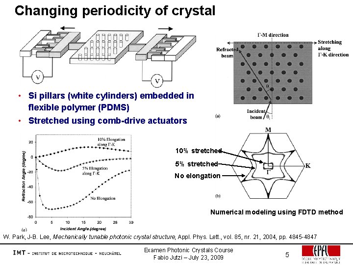
Changing periodicity of crystal • Si pillars (white cylinders) embedded in flexible polymer (PDMS) • Stretched using comb-drive actuators 10% stretched 5% stretched No elongation Numerical modeling using FDTD method W. Park, J-B. Lee, Mechanically tunable photonic crystal structure, Appl. Phys. Lett. , vol. 85, nr. 21, 2004, pp. 4845 -4847 Examen Photonic Crystals Course Fabio Jutzi – July 23, 2009 5

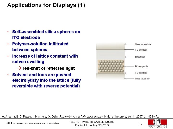
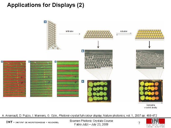
Applications for Displays (1) • Self-assembled silica spheres on ITO electrode • Polymer-solution infiltrated between spheres • Increase of lattice constant with solven swelling red-shift of reflected light • Solvent and ions are pushed electrolyticly into the lattice (fully reversible with reverse potential) A. Arsenault, D. Puzzo, I. Manners, G. Ozin, Photonic-crystal full-colour display, Nature photonics, vol. 1, 2007 pp. 468 -472 Examen Photonic Crystals Course Fabio Jutzi – July 23, 2009 6

Applications for Displays (2) A. Arsenault, D. Puzzo, I. Manners, G. Ozin, Photonic-crystal full-colour display, Nature photonics, vol. 1, 2007 pp. 468 -472 Examen Photonic Crystals Course Fabio Jutzi – July 23, 2009 7

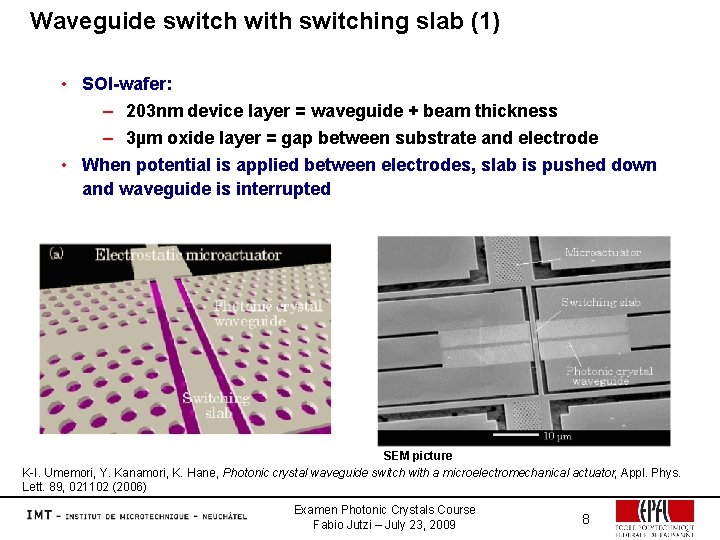
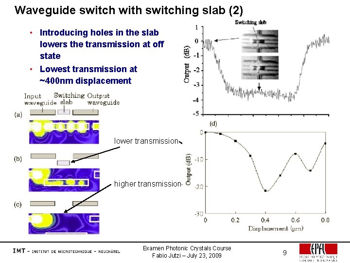
Waveguide switch with switching slab (1) • SOI-wafer: – 203 nm device layer = waveguide + beam thickness – 3µm oxide layer = gap between substrate and electrode • When potential is applied between electrodes, slab is pushed down and waveguide is interrupted SEM picture K-I. Umemori, Y. Kanamori, K. Hane, Photonic crystal waveguide switch with a microelectromechanical actuator, Appl. Phys. Lett. 89, 021102 (2006) Examen Photonic Crystals Course Fabio Jutzi – July 23, 2009 8

Waveguide switch with switching slab (2) • Introducing holes in the slab lowers the transmission at off state • Lowest transmission at ~400 nm displacement lower transmission higher transmission Examen Photonic Crystals Course Fabio Jutzi – July 23, 2009 9

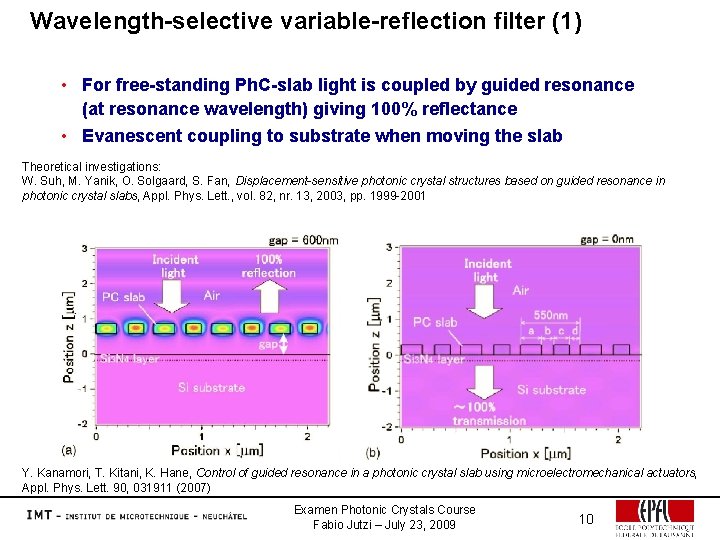
Wavelength-selective variable-reflection filter (1) • For free-standing Ph. C-slab light is coupled by guided resonance (at resonance wavelength) giving 100% reflectance • Evanescent coupling to substrate when moving the slab Theoretical investigations: W. Suh, M. Yanik, O. Solgaard, S. Fan, Displacement-sensitive photonic crystal structures based on guided resonance in photonic crystal slabs, Appl. Phys. Lett. , vol. 82, nr. 13, 2003, pp. 1999 -2001 Y. Kanamori, T. Kitani, K. Hane, Control of guided resonance in a photonic crystal slab using microelectromechanical actuators, Appl. Phys. Lett. 90, 031911 (2007) Examen Photonic Crystals Course Fabio Jutzi – July 23, 2009 10

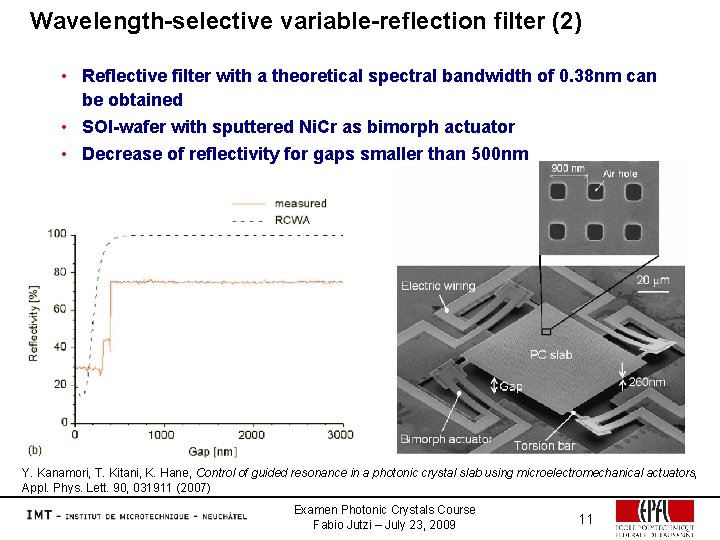
Wavelength-selective variable-reflection filter (2) • Reflective filter with a theoretical spectral bandwidth of 0. 38 nm can be obtained • SOI-wafer with sputtered Ni. Cr as bimorph actuator • Decrease of reflectivity for gaps smaller than 500 nm At gap > 5µm, resonant wavelength = 1545 nm Y. Kanamori, T. Kitani, K. Hane, Control of guided resonance in a photonic crystal slab using microelectromechanical actuators, Appl. Phys. Lett. 90, 031911 (2007) Examen Photonic Crystals Course Fabio Jutzi – July 23, 2009 11

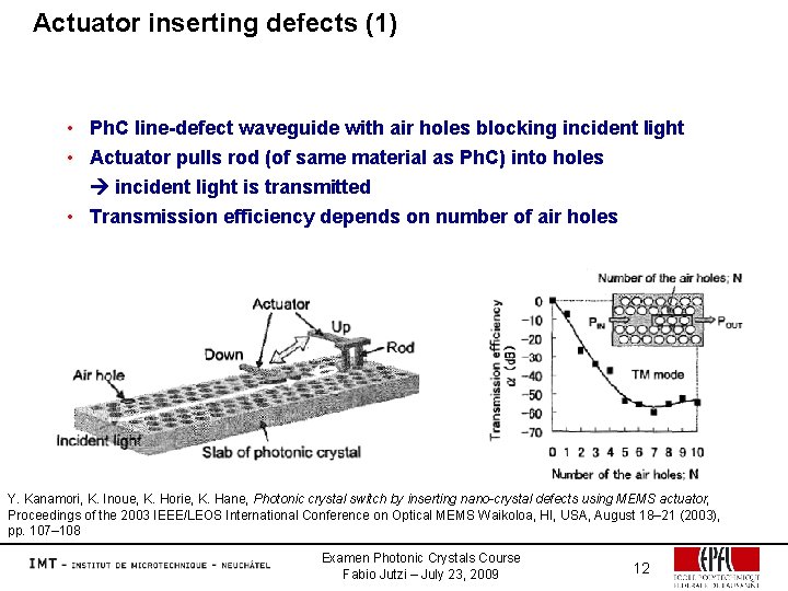
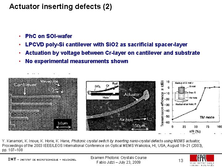
Actuator inserting defects (1) • Ph. C line-defect waveguide with air holes blocking incident light • Actuator pulls rod (of same material as Ph. C) into holes incident light is transmitted • Transmission efficiency depends on number of air holes Y. Kanamori, K. Inoue, K. Horie, K. Hane, Photonic crystal switch by inserting nano-crystal defects using MEMS actuator, Proceedings of the 2003 IEEE/LEOS International Conference on Optical MEMS Waikoloa, HI, USA, August 18– 21 (2003), pp. 107– 108 Examen Photonic Crystals Course Fabio Jutzi – July 23, 2009 12

Actuator inserting defects (2) • • Ph. C on SOI-wafer LPCVD poly-Si cantilever with Si. O 2 as sacrificial spacer-layer Actuation by voltage between Cr-layer on cantilever and substrate No experimental measurements shown Y. Kanamori, K. Inoue, K. Horie, K. Hane, Photonic crystal switch by inserting nano-crystal defects using MEMS actuator, Proceedings of the 2003 IEEE/LEOS International Conference on Optical MEMS Waikoloa, HI, USA, August 18– 21 (2003), pp. 107– 108 Examen Photonic Crystals Course Fabio Jutzi – July 23, 2009 13

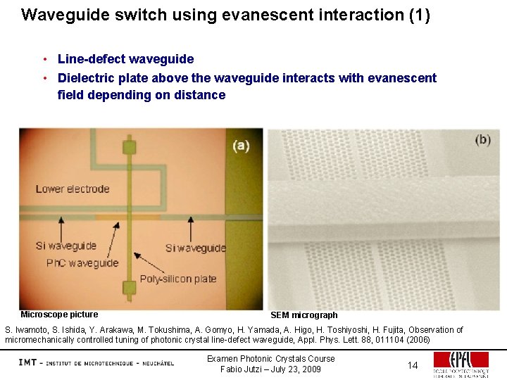
Waveguide switch using evanescent interaction (1) • Line-defect waveguide • Dielectric plate above the waveguide interacts with evanescent field depending on distance Microscope picture SEM micrograph S. Iwamoto, S. Ishida, Y. Arakawa, M. Tokushima, A. Gomyo, H. Yamada, A. Higo, H. Toshiyoshi, H. Fujita, Observation of micromechanically controlled tuning of photonic crystal line-defect waveguide, Appl. Phys. Lett. 88, 011104 (2006) Examen Photonic Crystals Course Fabio Jutzi – July 23, 2009 14

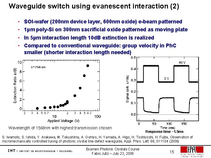
Waveguide switch using evanescent interaction (2) • • SOI-wafer (200 nm device layer, 600 nm oxide) e-beam patterned 1µm poly-Si on 300 nm sacrificial oxide patterned as moving plate In 5µm interaction length 10 d. B extinction is realized Compared to conventional waveguide: group velocity in Ph. C smaller (shorter interaction length needed) Wavelength of 1568 nm with highest transmission chosen Response time ~1. 5 ms S. Iwamoto, S. Ishida, Y. Arakawa, M. Tokushima, A. Gomyo, H. Yamada, A. Higo, H. Toshiyoshi, H. Fujita, Observation of micromechanically controlled tuning of photonic crystal line-defect waveguide, Appl. Phys. Lett. 88, 011104 (2006) Examen Photonic Crystals Course Fabio Jutzi – July 23, 2009 15

Conclusion • Different concept studies for mechanical tuning of Ph. C were shown • Not all are fabricated and completely measured • There is still lot to be done and optimized • Combining MEMS technology with Ph. C is very promising • Different possible applications: – Optical switchable filter – Display systems Examen Photonic Crystals Course Fabio Jutzi – July 23, 2009 16