Evolution of the Intel Architecture 8086 released in


 • Added floating point")


 C 2 t 2:")


 – ½")


 • Multi-core processors (started with 2 cores) – originally released")


- Slides: 37
Evolution of the Intel Architecture • 8086 released in 1978, ranged between 4 -10 MHz – 16 bit architecture which grew out of the earlier 8008 and 8080 architectures • mostly backward compatible with 8008, 8080 and 8085 – 20 -bit address space by • left shifting segment register 4 bits to be a 20 -bit base and adding index register as an offset – integer only, signed and unsigned • microcoded multiply and divide operations – CPU had 40 pins whose uses overlapped based on clock cycle • see next slide • pins and address/data bus are multiplexed (address during first cycle, data during second – fourth cycles) – floating point available by adding 8087 coprocessor
Notes: 3: add base address and offset 5: 4 -item instruction buffer (not for prefetching but because instruction lengths vary) 10: address bus 11 & 12: data and control buses
Addressing Modes and Execution Time • Each mode is listed as two numbers – 1 st for mov instruction, 2 nd for ALU • • • Register-register: 2, 3 Register-immediate: 4, 4 Register-memory: 8+EA, 9+EA Memory-register: 9+EA, 16+EA Memory-immediate: 10+EA, 17+EA – EA = time to compute effective address which ranges from 5 to 12 cycles – multiply ranged from 70 -160, divide from 80 -190 • For jump instructions: 11 (unconditional, no label), 15 (unconditional, labeled), 16 (conditional, labeled)
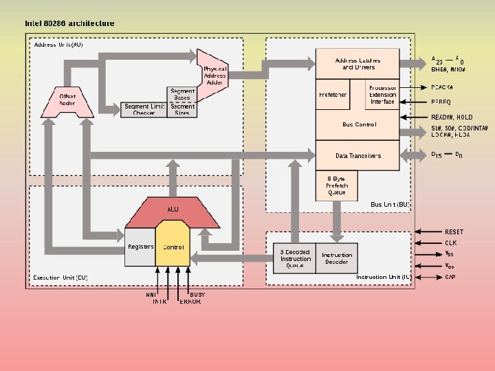
80286 • Introduced in 1982 – address and data bus and pins separated (no longer multiplexed) – protection capabilities to detect memory violations • two modes: real mode and protected mode (used to permit access to larger memory spaces, up to 4 GB) • this is because the 286 was designed for multiuser and multitasking systems (even though MS DOS and early versions of Windows were not) – ranged from 4 -25 MHz • performance averaged CPI of about 5 – still required a math coprocessor for FP (80287)
80386 • Released in 1985 • Extended the 286 architecture to 32 bits – all registers retained but “E” versions added to add the extra 16 bits • Third mode added (virtual mode multitasking) – added paging translation unit for virtual memory address translation • Added several new built-in data types: char, string, long int, boolean, pointer – still required math coprocessor for FP – Clock rates ranged from 12 MHz to 40 MHz
486 Processor • Added a pipeline (see next 2 slides) • Added floating point functional unit – no longer needed the math coprocessor – FP unit has its own bus to connect to FP registers – functional unit provided a degree of parallel processing in that while FP operations were executed, the pipeline would continue to fetch and execute integer operations • Added an atomic operation to better implement synchronization • Contained 8 KB combined instruction/data cache – later expanded to 16 KB • Clock rates range from 33 MHz to 100 MHz
The 486 Pipeline • 5 stages – Fetch 16 bytes worth of instruction • may be 1 instruction, part of 1 instruction, multiple instructions – Decode stage 1 – examine 16 bytes to identify whole instruction • if buffer does not contain entire instruction, stall pipeline and continue fetching instruction • divide 16 bytes into instruction(s) (find the end of each instruction) – Decode stage 2 – decode the next instruction • includes fetching operands from registers – Execution – ALU operations, branch operations, cache (mov) instructions • may take multiple cycles if ALU operation requires multiple cycles (*, /, FP) or requires 1 (or more) memory accesses • further stalls needed if memory access is a cache miss – Write result of load or ALU operation to register
486 Difficulties • Stalls arise for numerous reasons – 17 byte long instructions require 2 instruction fetch stages – ALU memory-register/memory-immediate takes at least 1 additional cycle • possibly two if memory item is both source and destination • such a situation stalls instructions in the decode 2 stage • or if there is a cache miss – Complex addressing modes can cause stalls • pointer accessing (indirect addressing) takes 2 memory accesses • scaled addressing mode involves both a shift and an add • again, stalls occur in the decode 2 stage – Branch instructions have a 3 cycle penalty • branches are computed in the EX stage (4 th stage) • some loop operations take more than 1 cycle to compute adding a further stall
• Example 1: – three data movements, no stalls • Example 2: – data hazard, 1 cycle of stall • Example 3: – branch penalty 486 Examples
486 Overall Architecture
Pentium Architecture • Summarizing problems with the 486 pipeline – variable length instructions, variable complexity of operations, memory-register ALU operations, indirect addressing – to improve performance using RISC features, Pentium (586) architects needed to rethink things while still implementing backward compatibility • CISC architectures handle the fetch-execute cycle through a microprogrammed control unit – a microprogram consists of a sequence of microinstructions, each being of equal length and taking 1 clock cycle (usually) to execute • Re-implement the pipeline as follows – continue to use an instruction fetch unit to fill a buffer with instructions – use a separate decode unit to identify each instruction and decode it into microcode – issue microinstructions to a pipeline
Control and Micro-Operations • An example architecture is shown to the right • Each of the various connections is controlled by a particular control signal – MBR to the AC controlled with signal C 11 – PC to MAR by C 2 – AC to ALU C 7 • note that this figure is incomplete • A microprogram is a sequence of microoperations this is not an x 86 architecture!
Example • Consider a CISC instruction such as Add R 1, X – X copied into MAR and a memory read signaled – datum returned across data bus to MBR – adder sent values in R 1 and MBR, adding the two, storing result back into R 1 • This sequence can be written in terms of microoperations as: t 1 – t 5 are clock cycles, each – – – t 1: t 2: t 3: t 4: MAR (IR (address) ) MBR Memory R 1 (R 1) + (MBR) Acc (R 1) + (MBR) R 1 (Acc) microinstruction executes in separate clock cycles • Each micro-operation is handled by one or more control signals – For instance, MBR Memory is C 5
Control Memory Each microprogram consists of one or more microinstructions, each stored in a separate entry of the control memory The control memory itself is firmware, a program stored in ROM, that is placed inside of the control unit . . . Jump to Indirect or Execute. . . Jump to Fetch Jump to Op code routine. . . Jump to Fetch or Interrupt Fetch cycle routine Indirect Cycle routine Interrupt cycle routine Execute cycle begin AND routine ADD routine Note: each micro-program ends with a branch to the Fetch, Interrupt, Indirect or Execute micro-program
Example of Three Micro-Programs • Fetch: t 1: MAR (PC) C 2 t 2: MBR Memory C 0, C 5, CR PC (PC) + 1 C* t 3: IR (MBR) C 4 • Indirect: t 1: MAR (IR (address) ) C 8 t 2: MBR Memory C 0, C 5, CR t 3: IR(address) (MBR (address) ) C 4 • Interrupt: t 1: MBR (PC) C 1 t 2: MAR save address C* PC routine address C* t 3: Memory (MBR) C 12, CW – CR – Read control to system bus – CW – write control to system bus • C 0 – C 12 refers to the previous figure • C* are signals not shown in the figure
Horizontal vs. Vertical Micro-Instructions Micro-instruction address points to a branch in the control memory and is taken if the condition bit is true Micro-instruction Address Function Codes Vertical micro-instructions use function codes that need additional decoding Internal CPU Control Signals Jump Condition Horizontal micro-instructions contain 1 bit for every control signal controlled by the control unit Micro-instruction Address This micro-instruction requires 1 bit for every control line, it is longer than Jump Condition the vertical micro-instruction and System Bus therefore takes more space to store, Control Signals but does not require additional time to decode by the control unit
Micro-programmed Control Unit
Continued • Decoder analyzes IR – delivers starting address of op code’s micro-program in control store • address placed in the to a micro-program counter (here, called a Control Address Register) • Loop on the following – sequencer signals read of control memory using address in micro. PC – item in control memory moved to control buffer register – contents of control buffer register generate control signals and next address information • if the micro-instructions are vertical, decoding is required here – sequencer moves next address to control address register • next instruction (add 1 to current) • jump to new part of this microprogram • jump to new machine routine
Pentium Architectures • Pentium I released 1993 – upgraded to 64 -bit data bus – superscalar 5 -stage pipeline (2 parallel pipelines) – branch speculation added – separate instruction and data catches – FP portion of the processor had an infamous bug requiring the entire CPU be replaced! • Pentium II released 1995 – added L 2 cache • Pentium III released 1999 – both PII and PIII used 14 -stage pipelines • Pentium IV released 2000 – superscalar expanded to 3 parallel pipelines – 21 -31 stage pipeline
Pentium IV: RISC features • RISC features implemented on microinstructions • • • – instead of machine instructions Microinstruction-level pipeline Dynamically scheduled micro-operations Reservation stations (128) Multiple functional units (7) Branch speculation via branch target buffer – speculation at micro-instruction level • instead of an ROB, decisions made at the reservation stations • miss-speculation causes reservation stations to flush their contents • correct speculation causes reservation stations to forward results to registers/store units – trace cache used (discussed shortly)
Pentium II-III Pipeline • IF unit: 3 stages • ID unit: 2 stages • Issue unit: 2 stages – up to 3 microinstructions issued per cycle – register renaming occurs here – instructions sent to reservation station • Execution units: 1 -32 stages – 1 for int, up to 32 for FP • Write back: 3 stages • Commit: 3 stages – up to 3 microinstructions can commit in any cycle
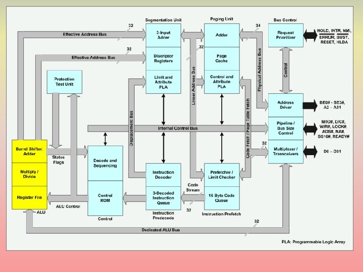
Pentium IV Overall Architecture
Specifications • 7 functional units: – 2 simple ALUs (add, compare, shift) – ½ cycle execution to accommodate up to 2 micro-operations per cycle – 1 complex ALU (integer multiplication and division) – multicycle, pipelined – 1 load unit and 1 store unit – including address computation – 1 FP move (register to register move and convert) – 1 FP arithmetic unit (+, -, *, /) – multicycle, pipelined, some SIMD execution permitted on these units • 128 registers for renaming – reservation stations are used rather than a re-order buffer – instructions must wait in reservation stations longer than in Tomasulo’s version, waiting for speculation results
Trace Cache • Instruction cache – caches blocks of instructions recently executed together • Trace cache encodes branch behavior implicitly • Miss-speculated instructions would be discarded from the cache – stores microinstructions (not machine instructions) • Combining a trace cache and branch target buffer minimizes microinstruction fetch and decoding – as long as the microinstructions remain in the trace cache Miss-predictions at the microinstruction level are far rarer than miss-predictions at the machine level
Source of Stalls • Process breaks down as follows – in the issue stage • branch miss-predictions • cache misses, particularly trace cache miss • reservation stations full • limited number of entries in the commit buffer • less than 3 instructions fetched in 1 cycle • less than 3 microinstructions can be issued at the time – at the commit stage • branch miss-predictions • instructions not ready to commit yet • branch computation not yet available
Continued • Miss-prediction of microinstruction are very infrequent (about. 8% for int, . 1% for FP) – FP are often more predictable because they involve a lot of for loops – machine language level miss-speculation between. 1% and 1. 5% • Trace cache has nearly a 0% miss rate – L 1 and L 2 data caches have miss rates of around 6% and. 5% respectively – machine’s effective CPI ranges from around 1. 2 to 5. 85 with an average of around 2. 2 • machine instructions, not micro-operations
Intel Core (i. Core) • Multi-core processors (started with 2 cores) – originally released with two cores where one was disabled • Same basic architecture as Pentium III but with lower clock rates, this was offset by several new innovations – issue up to 4 microinstructions at a time – more efficient decode stages • using macro-ops which attempts to combine two micro-instructions into a single one such as a compare and conditional branch – more efficient execution units • one cycle throughput due to pipelined ALU units (previously had a 2 -cycle throughput) – larger caches and buses – no SMT processing (developed for Pentium IV) – lower power consumption (needed when there are multiple cores) – i. Core has released processors of 1, 2, 4 and 6 cores
Intel Core i 7 • Aggressive out of order speculation – pipeline reduced from 31 to 14 stages • Instruction fetch unit – retrieves 16 bytes to decode • feeds a queue that can store up to 18 instructions at a time – multilevel branch target buffer, return address stack for speculation • miss-predictions cause a penalty of about 15 cycles – 32 KB instruction cache – if a loop is detected that contains fewer than 28 instructions or 256 bytes • these instructions will remain in a buffer to repeatedly be issued (rather than repeated instruction fetches)
Continued • Decoding converts machine instructions into microcode using any of four decoders – simple micro-operation instructions (2 each) – complex micro-operation instructions (2 each) • Instruction issue can issue up to 6 microoperations per cycle to – 36 centralized reservation stations – 6 functional units including 1 load and 2 store units that share a memory buffer connected to 3 different data caches
i 7 Architecture
i 7 Performance CPI for various SPEC 06 benchmarks Average CPI is 1. 06 for integer programs and. 89 for FP (machine instructions, not micro-instructions) i 7 susceptible to miss-speculation resulting in “wasted” work Up to 40% of the total work that goes into Spec 06 benchmarks is wasted Waste also arises from cache misses (10 cycles or more lost with an L 1 miss, 30 -40 for L 2 misses and as much as 135 for L 3 misses)
Multicore Processors • Each core is a separate processor with its own registers, ALU, control unit, local bus, and L 1 cache – L 2 cache is shared among all cores – L 3 off chip may be added – performance of multicore processors shown below • speedup is close to but not always linear to the number of cores
A Balancing Act • Improving one aspect of our processor does not necessarily improve performance – it might actually harm performance • lengthening pipeline depth, increasing clock speed in the P 4 without adding reservation stations or using a trace cache degrades performance • stalls arise at issue stage due to needing more instructions to issue • cache misses have greater impact when the clock speed is increased • without accurate branch prediction and speculation hardware, stalls from miss-predicted branches can have a tremendous impact on performance • we saw this in both the ARM and i 7 processors
Continued • As clock speeds increase – stalls from cache misses create a bigger impact on CPI – larger caches and cache optimization techniques are needed • To support multiple issue of instructions – need larger cache-to-processor bandwidth • Increasing instruction issue rate – requires a proportional increase in the number of reservation stations and reorder buffer size