Evolution of Intels transistor technology 45 nm 14


![3. The 22 nm 3 D Tri-Gate transistor-2 The traditional planar transistor [82] 3. The 22 nm 3 D Tri-Gate transistor-2 The traditional planar transistor [82]](https://slidetodoc.com/presentation_image_h/19a3a6173a11f1f3f259a3c380d1f710/image-16.jpg)
![3. The 22 nm 3 D Tri-Gate transistor-4 The 22 nm Tri-Gate transistor-3 [82] 3. The 22 nm 3 D Tri-Gate transistor-4 The 22 nm Tri-Gate transistor-3 [82]](https://slidetodoc.com/presentation_image_h/19a3a6173a11f1f3f259a3c380d1f710/image-18.jpg)
![3. The 22 nm 3 D Tri-Gate transistor-7 Intel’s 22 nm manufacturing fabs [82] 3. The 22 nm 3 D Tri-Gate transistor-7 Intel’s 22 nm manufacturing fabs [82]](https://slidetodoc.com/presentation_image_h/19a3a6173a11f1f3f259a3c380d1f710/image-21.jpg)

- Slides: 29

Evolution of Intel’s transistor technology 45 nm – 14 nm Dezső Sima Vers. 1. 1 September 2015

Contents • 1. Overview of the evolution of Intel’s basic microarchitectures • 2. The high-k + metal gate transistor • 3. The 22 nm 3 D Tri-Gate transistor • 4. The 14 nm 3 D Tri-Gate transistor

1. Overview of the evolution of Intel’s basic microarchitectures

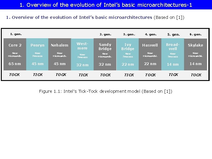
1. Overview of the evolution of Intel’s basic microarchitectures-1 1. Overview of the evolution of Intel’s basic microarchitectures (Based on [1]) 1. gen. 2. gen. 3. gen. 4. gen. 5. gen. 6. gen. Westmere Sandy Bridge Ivy Bridge Haswell Broadwell Skylake New Process New Microarchi. Core 2 Penryn Nehalem New Microarch. New Process New Microarch. 65 nm 45 nm 32 nm 22 nm 14 nm TOCK TICK TOCK Figure 1. 1: Intel’s Tick-Tock development model (Based on [1])

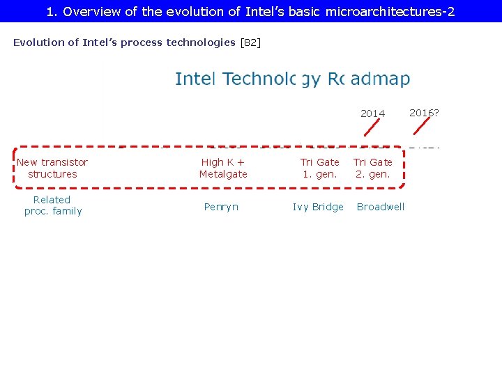
1. Overview of the evolution of Intel’s basic microarchitectures-2 Evolution of Intel’s process technologies [82] 2014 New transistor structures High K + Metalgate Tri Gate 1. gen. Related proc. family Penryn Ivy Bridge Tri Gate 2. gen. Broadwell 2016?

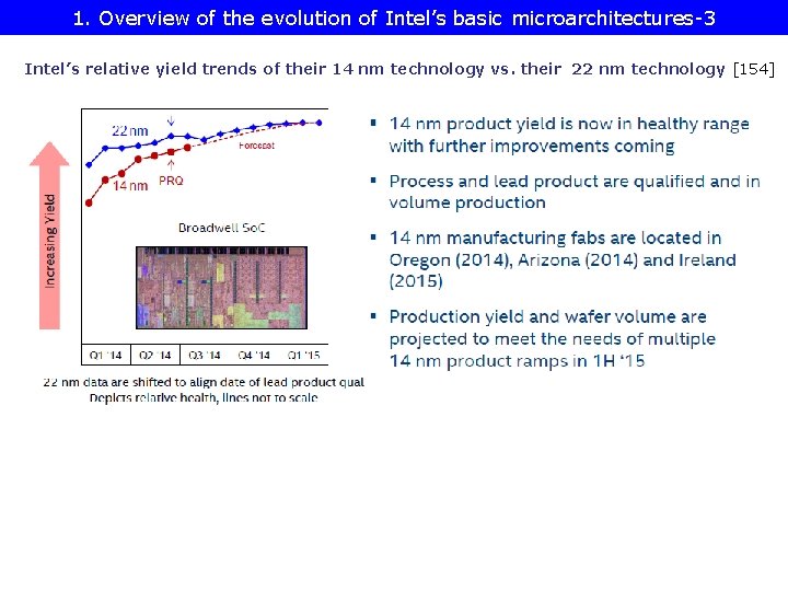
1. Overview of the evolution of Intel’s basic microarchitectures-3 Intel’s relative yield trends of their 14 nm technology vs. their 22 nm technology [154]

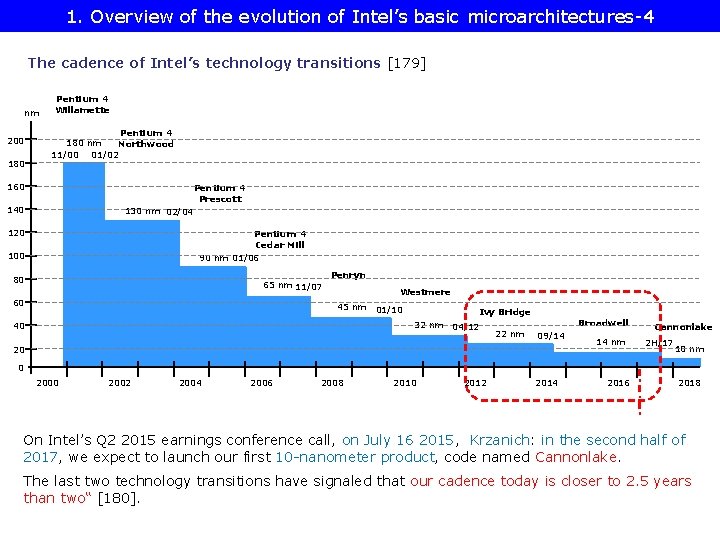
1. Overview of the evolution of Intel’s basic microarchitectures-4 The cadence of Intel’s technology transitions [179] nm 200 180 Pentium 4 Willamette Pentium 4 180 nm Northwood 11/00 01/02 160 Pentium 4 Prescott 140 130 nm 02/04 120 Pentium 4 Cedar Mill 90 nm 01/06 100 80 65 nm 11/07 60 Penryn Westmere 45 nm 01/10 Ivy Bridge 32 nm 40 04/12 22 nm Broadwell 09/14 20 14 nm Cannonlake 2 H/17 10 nm 0 2002 2004 2006 2008 2010 2012 2014 2016 2018 On Intel’s Q 2 2015 earnings conference call, on July 16 2015, Krzanich: in the second half of 2017, we expect to launch our first 10 -nanometer product, code named Cannonlake. The last two technology transitions have signaled that our cadence today is closer to 2. 5 years than two“ [180].

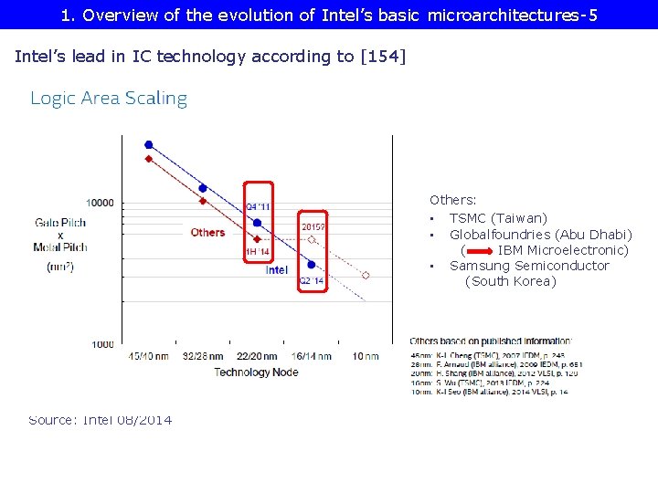
1. Overview of the evolution of Intel’s basic microarchitectures-5 Intel’s lead in IC technology according to [154] Others: • TSMC (Taiwan) • Globalfoundries (Abu Dhabi) ( IBM Microelectronic) • Samsung Semiconductor (South Korea) Source: Intel 08/2014

2. The high-k + metal gate transistor

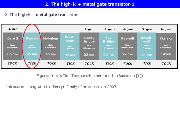
2. The high-k + metal gate transistor-1 2. The high-k + metal gate transistor 1. gen. 2. gen. 3. gen. 4. gen. 5. gen. 6. gen. Westmere Sandy Bridge Ivy Bridge Haswell Broadwell Skylake New Process New Microarchi. Core 2 Penryn Nehalem New Microarch. New Process New Microarch. 65 nm 45 nm 32 nm 22 nm 14 nm TOCK TICK TOCK Figure: Intel’s Tick-Tock development model (Based on [1]) Introduced along with the Penryn family of processors in 2007.

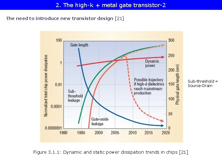
2. The high-k + metal gate transistor-2 The need to introduce new transistor design [21] Sub-threshold = Source-Drain Figure 3. 1. 1: Dynamic and static power dissipation trends in chips [21]

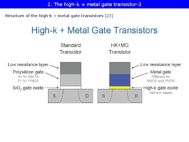
2. The high-k + metal gate transistor-3 Structure of the high-k + metal gate transistors [23]

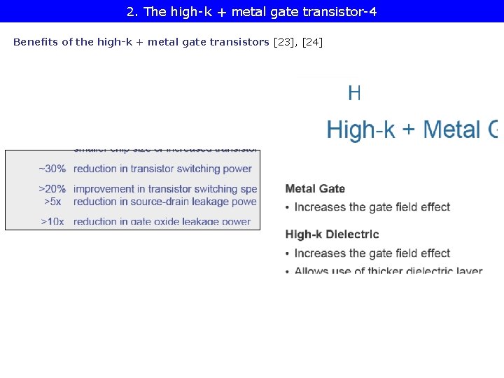
2. The high-k + metal gate transistor-4 Benefits of the high-k + metal gate transistors [23], [24]

3. The 22 nm 3 D Tri-Gate transistor

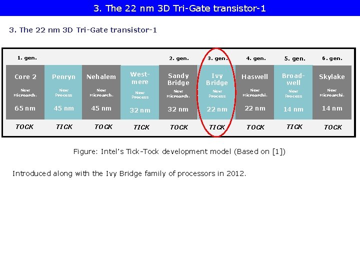
3. The 22 nm 3 D Tri-Gate transistor-1 1. gen. 2. gen. 3. gen. 4. gen. 5. gen. 6. gen. Westmere Sandy Bridge Ivy Bridge Haswell Broadwell Skylake New Process New Microarchi. Core 2 Penryn Nehalem New Microarch. New Process New Microarch. 65 nm 45 nm 32 nm 22 nm 14 nm TOCK TICK TOCK Figure: Intel’s Tick-Tock development model (Based on [1]) Introduced along with the Ivy Bridge family of processors in 2012.
![3 The 22 nm 3 D TriGate transistor2 The traditional planar transistor 82 3. The 22 nm 3 D Tri-Gate transistor-2 The traditional planar transistor [82]](https://slidetodoc.com/presentation_image_h/19a3a6173a11f1f3f259a3c380d1f710/image-16.jpg)
3. The 22 nm 3 D Tri-Gate transistor-2 The traditional planar transistor [82]

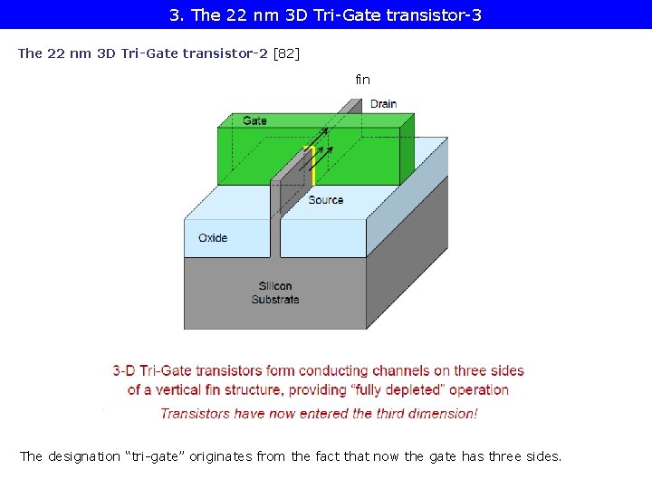
3. The 22 nm 3 D Tri-Gate transistor-3 The 22 nm 3 D Tri-Gate transistor-2 [82] fin The designation “tri-gate” originates from the fact that now the gate has three sides.
![3 The 22 nm 3 D TriGate transistor4 The 22 nm TriGate transistor3 82 3. The 22 nm 3 D Tri-Gate transistor-4 The 22 nm Tri-Gate transistor-3 [82]](https://slidetodoc.com/presentation_image_h/19a3a6173a11f1f3f259a3c380d1f710/image-18.jpg)
3. The 22 nm 3 D Tri-Gate transistor-4 The 22 nm Tri-Gate transistor-3 [82]

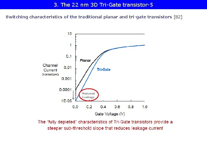
3. The 22 nm 3 D Tri-Gate transistor-5 Switching characteristics of the traditional planar and tri-gate transistors [82]

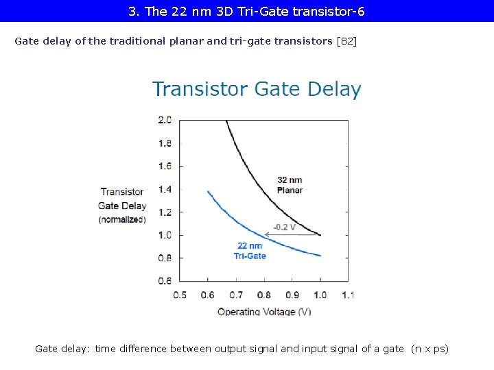
3. The 22 nm 3 D Tri-Gate transistor-6 Gate delay of the traditional planar and tri-gate transistors [82] Gate delay: time difference between output signal and input signal of a gate (n x ps)
![3 The 22 nm 3 D TriGate transistor7 Intels 22 nm manufacturing fabs 82 3. The 22 nm 3 D Tri-Gate transistor-7 Intel’s 22 nm manufacturing fabs [82]](https://slidetodoc.com/presentation_image_h/19a3a6173a11f1f3f259a3c380d1f710/image-21.jpg)
3. The 22 nm 3 D Tri-Gate transistor-7 Intel’s 22 nm manufacturing fabs [82]

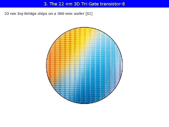
3. The 22 nm 3 D Tri-Gate transistor-8 22 nm Ivy Bridge chips on a 300 mm wafer [82]

4. The 14 nm 3 D Tri-Gate transistor

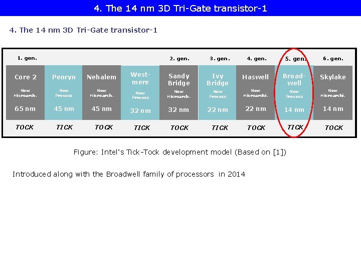
4. The 14 nm 3 D Tri-Gate transistor-1 1. gen. 2. gen. 3. gen. 4. gen. 5. gen. 6. gen. Westmere Sandy Bridge Ivy Bridge Haswell Broadwell Skylake New Process New Microarchi. Core 2 Penryn Nehalem New Microarch. New Process New Microarch. 65 nm 45 nm 32 nm 22 nm 14 nm TOCK TICK TOCK Figure: Intel’s Tick-Tock development model (Based on [1]) Introduced along with the Broadwell family of processors in 2014

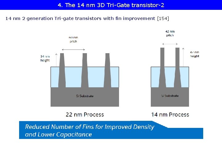
4. The 14 nm 3 D Tri-Gate transistor-2 14 nm 2 generation Tri-gate transistors with fin improvement [154]

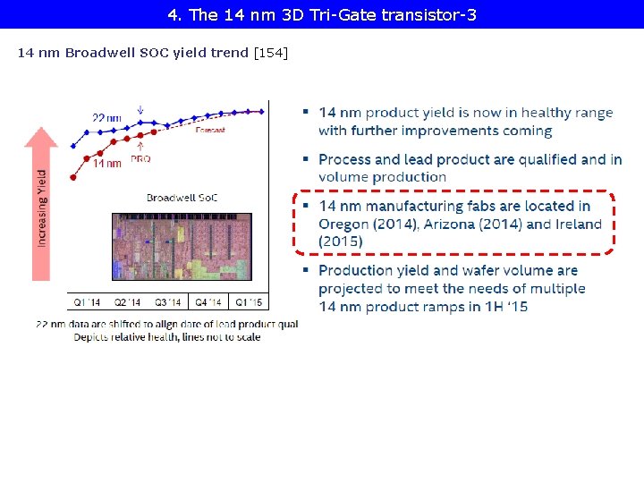
4. The 14 nm 3 D Tri-Gate transistor-3 14 nm Broadwell SOC yield trend [154]

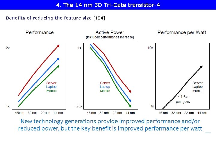
4. The 14 nm 3 D Tri-Gate transistor-4 Benefits of reducing the feature size [154]

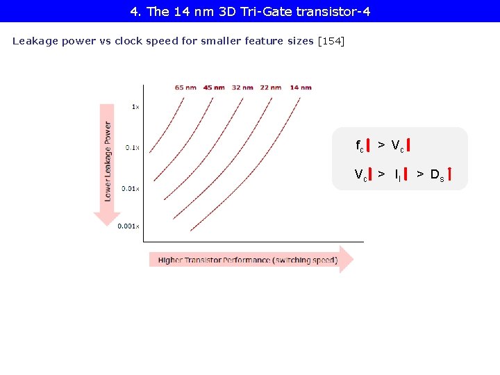
4. The 14 nm 3 D Tri-Gate transistor-4 Leakage power vs clock speed for smaller feature sizes [154] fc > Vc Vc > I l > Ds

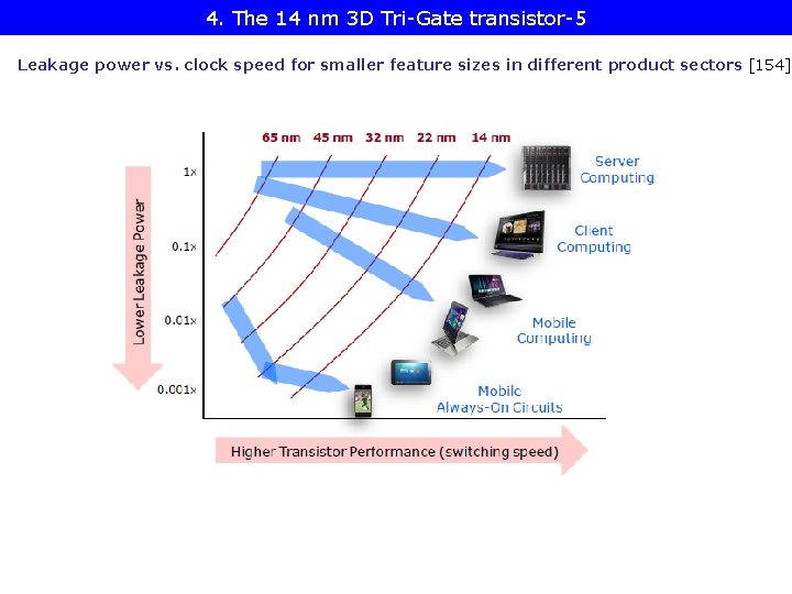
4. The 14 nm 3 D Tri-Gate transistor-5 Leakage power vs. clock speed for smaller feature sizes in different product sectors [154]