Evolution of Intels Basic Microarchitectures 2 Dezs Sima
Evolution of Intel’s Basic Microarchitectures - 2 Dezső Sima Vers. 3. 3 April 2013
Contents • 1. Introduction • 2. Core 2 • 3. Penryn • 4. Nehalem • 5. Nehalem-EX • 6. Westmere • 7. Westmere-EX
Contents • 8. Sandy Bridge • 9. Sandy Bridge Extreme Edition • 10. Ivy Bridge • 11. Haswell • 12. Overview of the evolution
8. Sandy Bridge • 8. 1 Introduction • 8. 2 Advanced Vector Extension (AVX) • 8. 3 On-die ring interconnect bus • 8. 4 On-die integrated graphics unit • 8. 5 Enhanced turbo boost technology
8. 1 Introduction (1) 8. 1 Introduction • Sandy Bridge is Intel’s new microarchitecture using 32 nm line width. • First delivered in 1/2011
![8. 1 Introduction (2) Main functional units of Sandy Bridge [143] Part 4 256 8. 1 Introduction (2) Main functional units of Sandy Bridge [143] Part 4 256](http://slidetodoc.com/presentation_image/922db7a576aee110ccfc0479cb511247/image-6.jpg)
8. 1 Introduction (2) Main functional units of Sandy Bridge [143] Part 4 256 KB L 2 (9 clk) Hyperthreading 32 K L 1 D (3 clk) AES Instr. AVX 256 bit VMX Unrestrict. 4 Operands 20 nm 2 / Core 8 MB @ 1. 0 1. 4 GHz (to L 3 connected) (25 clk) 256 b/cycle Ring Architecture DDR 3 -1600 32 nm process / ~225 nm 2 die size / 85 W TDP PCIe 2. 0 25. 6 GB/s
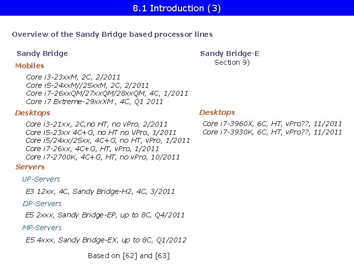
8. 1 Introduction (3) Overview of the Sandy Bridge based processor lines Sandy Bridge-E Section 9) Sandy Bridge Mobiles Core i 3 -23 xx. M, 2 C, 2/2011 i 5 -24 xx. M//25 xx. M, 2 C, 2/2011 i 7 -26 xx. QM/27 xx. QM/28 xx. QM, 4 C, 1/2011 i 7 Extreme-29 xx. XM , 4 C, Q 1 2011 Desktops Core i 3 -21 xx, 2 C, no HT, no v. Pro, 2/2011 Core i 5 -23 xx 4 C+G, no HT no VPro, 1/2011 Core i 5/24 xx/25 xx, 4 C+G, no HT, v. Pro, 1/2011 Core i 7 -26 xx, 4 C+G, HT, v. Pro, 1/2011 Core i 7 -2700 K, 4 C+G, HT, no v. Pro, 10/2011 Servers UP-Servers E 3 12 xx, 4 C, Sandy Bridge-H 2, 4 C, 3/2011 DP-Servers E 5 2 xxx, Sandy Bridge-EP, up to 8 C, Q 4/2011 MP-Servers E 5 4 xxx, Sandy Bridge-EX, up to 8 C, Q 1/2012 Based on [62] and [63] Core i 7 -3960 X, 6 C, HT, v. Pro? ? , 11/2011 Core i 7 -3930 K, 6 C, HT, v. Pro? ? , 11/2011
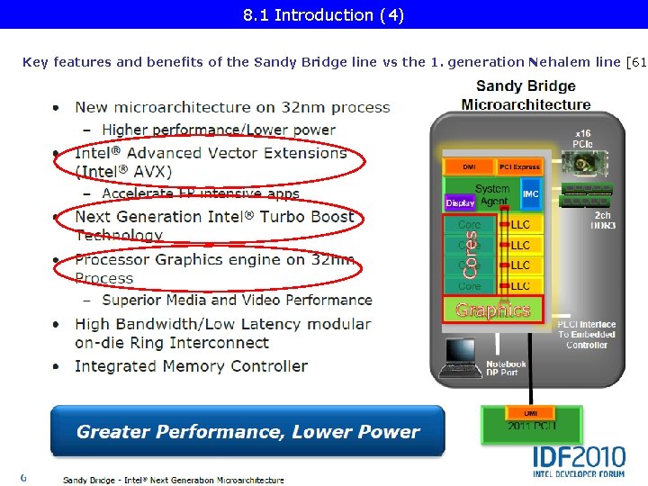
8. 1 Introduction (4) Key features and benefits of the Sandy Bridge line vs the 1. generation Nehalem line [61]
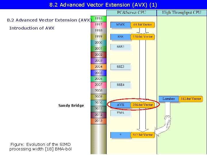
8. 2 Advanced Vector Extension (AVX) (1) 8. 2 Advanced Vector Extension (AVX) Introduction of AVX Sandy Bridge Figure: Evolution of the SIMD processing width [18] BMA-ból
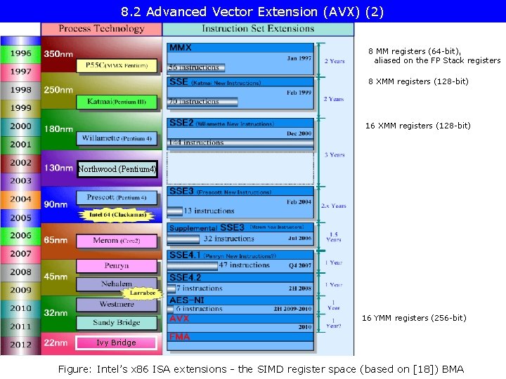
8. 2 Advanced Vector Extension (AVX) (2) 8 MM registers (64 -bit), aliased on the FP Stack registers 8 XMM registers (128 -bit) 16 XMM registers (128 -bit) Northwood (Pentium 4) Norhwood Northwood (Pentium 4) 16 YMM registers (256 -bit) Ivy Bridge Figure: Intel’s x 86 ISA extensions - the SIMD register space (based on [18]) BMA
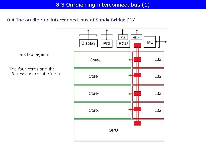
8. 3 On-die ring interconnect bus (1) 8. 4 The on die ring interconnect bus of Sandy Bridge [66] Six bus agents. The four cores and the L 3 slices share interfaces.
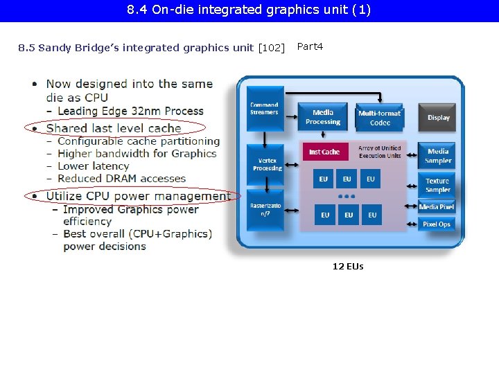
8. 4 On-die integrated graphics unit (1) 8. 5 Sandy Bridge’s integrated graphics unit [102] Part 4 12 EUs
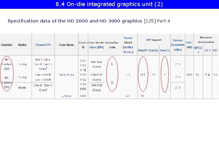
8. 4 On-die integrated graphics unit (2) Specification data of the HD 2000 and HD 3000 graphics [125] Part 4 -
![8. 4 On-die integrated graphics unit (3) Performance comparison: gaming [126] part 4 HD 8. 4 On-die integrated graphics unit (3) Performance comparison: gaming [126] part 4 HD](http://slidetodoc.com/presentation_image/922db7a576aee110ccfc0479cb511247/image-14.jpg)
8. 4 On-die integrated graphics unit (3) Performance comparison: gaming [126] part 4 HD 5570 400 ALUs i 5/i 7 2 xxx/3 xxx: Sandy Bridge i 5 6 xx Arrandale frames per sec
![8. 5 Enhanced turbo boost technology (1) 8. 5 Enhanced turbo boost technology [64] 8. 5 Enhanced turbo boost technology (1) 8. 5 Enhanced turbo boost technology [64]](http://slidetodoc.com/presentation_image/922db7a576aee110ccfc0479cb511247/image-15.jpg)
8. 5 Enhanced turbo boost technology (1) 8. 5 Enhanced turbo boost technology [64] Innovative concept of the 2. 0 generation Turbo Boost technology The concept utilizes the real temperature response of processors to power changes in order to increase the extent of overclocking [64] Cooler Thermal capacitance
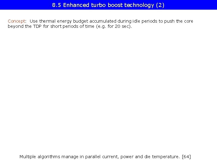
8. 5 Enhanced turbo boost technology (2) Concept: Use thermal energy budget accumulated during idle periods to push the core beyond the TDP for short periods of time (e. g. for 20 sec). Multiple algorithms manage in parallel current, power and die temperature. [64]
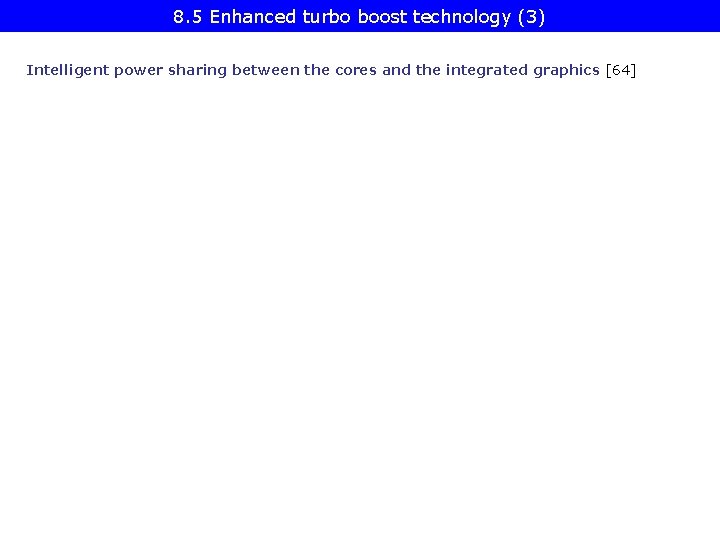
8. 5 Enhanced turbo boost technology (3) Intelligent power sharing between the cores and the integrated graphics [64]
![8. 5 Enhanced turbo boost technology (4) NHM/M NHM/D [61] WSM/M WSM/D 8. 5 Enhanced turbo boost technology (4) NHM/M NHM/D [61] WSM/M WSM/D](http://slidetodoc.com/presentation_image/922db7a576aee110ccfc0479cb511247/image-18.jpg)
8. 5 Enhanced turbo boost technology (4) NHM/M NHM/D [61] WSM/M WSM/D
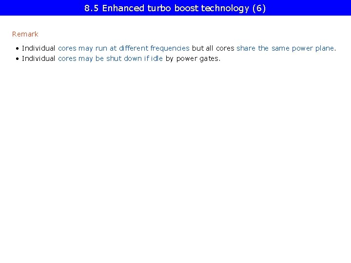
8. 5 Enhanced turbo boost technology (6) Remark • Individual cores may run at different frequencies but all cores share the same power plane. • Individual cores may be shut down if idle by power gates.

9. The Sandy Bridge-E line
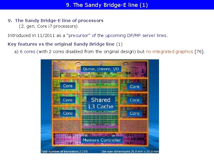
9. The Sandy Bridge-E line (1) 9. The Sandy Bridge-E line of processors (2. gen. Core i 7 processors) Introduced in 11/2011 as a “precursor” of the upcoming DP/MP server lines. Key features vs the original Sandy Bridge line (1) a) 6 cores (with 2 cores disabled from the original design) but no integrated graphics [76].
![9. The Sandy Bridge-E line (2) Sandy Bridge E [76] 32 nm 435 mm 9. The Sandy Bridge-E line (2) Sandy Bridge E [76] 32 nm 435 mm](http://slidetodoc.com/presentation_image/922db7a576aee110ccfc0479cb511247/image-22.jpg)
9. The Sandy Bridge-E line (2) Sandy Bridge E [76] 32 nm 435 mm 2 2. 27 B trs 15 MB L 3 Sandy Bridge (2 x) [61] 32 nm 216 mm 2 995 mtrs 8 MB L 3
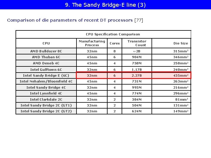
9. The Sandy Bridge-E line (3) Comparison of die parameters of recent DT processors [77] CPU Specification Comparison CPU Manufacturing Process Cores Transistor Count Die Size AMD Bulldozer 8 C 32 nm 8 ~2 B 315 mm 2 AMD Thuban 6 C 45 nm 6 904 M 346 mm 2 AMD Deneb 4 C 45 nm 4 758 M 258 mm 2 Intel Gulftown 6 C 32 nm 6 1. 17 B 240 mm 2 Intel Sandy Bridge E (6 C) 32 nm 6 2. 27 B 435 mm 2 Intel Nehalem/Bloomfield 4 C 45 nm 4 731 M 263 mm 2 Intel Sandy Bridge 4 C 32 nm 4 995 M 216 mm 2 Intel Lynnfield 4 C 45 nm 4 774 M 296 mm 2 Intel Clarkdale 2 C 32 nm 2 384 M 81 mm 2 Intel Sandy Bridge 2 C (GT 1) 32 nm 2 504 M 131 mm 2 Intel Sandy Bridge 2 C (GT 2) 32 nm 2 624 M 149 mm 2
![9. The Sandy Bridge-E line (4) Cache/memory latencies of recent DT processors [77] Bulldozer 9. The Sandy Bridge-E line (4) Cache/memory latencies of recent DT processors [77] Bulldozer](http://slidetodoc.com/presentation_image/922db7a576aee110ccfc0479cb511247/image-24.jpg)
9. The Sandy Bridge-E line (4) Cache/memory latencies of recent DT processors [77] Bulldozer Sandy Bridge-E L 1 L 2 L 3 Main Memory AMD FX-8150 (3. 6 GHz) 4 21 65 195 AMD Phenom II X 4 975 BE (3. 6 GHz) 3 15 59 182 AMD Phenom II X 6 1100 T (3. 3 GHz) 3 14 55 157 Intel Core i 5 2500 K (3. 3 GHz) 4 11 25 148 Intel Core i 7 3960 X (3. 3 GHz) 4 11 30 167
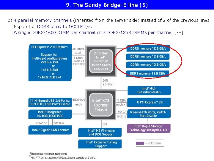
9. The Sandy Bridge-E line (5) b) 4 parallel memory channels (inherited from the server side) instead of 2 of the previous lines. Support of DDR 3 of up to 1600 MT/s. A single DDR 3 -1600 DIMM per channel or 2 DDR 3 -1333 DIMMs per channel [78].
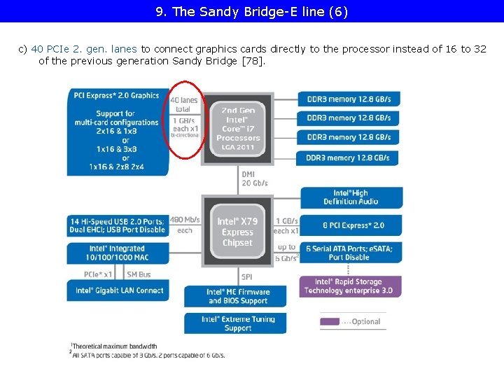
9. The Sandy Bridge-E line (6) c) 40 PCIe 2. gen. lanes to connect graphics cards directly to the processor instead of 16 to 32 of the previous generation Sandy Bridge [78].
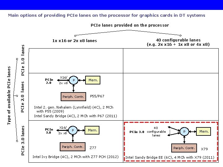
Main options of providing PCIe lanes on the processor for graphics cards in DT systems PCIe lanes provided on the processor PCIe 1. 0 lanes PCIe 2. 0 lanes PCIe 3. 0 lanes Type of available PCIe lanes 1 x x 16 or 2 x x 8 lanes PCIe 2. 0 X 16/ 2 x x 8 P Periph. Contr. 40 configurable lanes (e. g. 2 x x 16 + 1 x x 8 or 4 x x 8) Mem. P 55/P 67 Intel 2. gen. Nehalem (Lynnfield) (4 C), 2 MCh with P 55 (2009) Intel Sandy Bridge (4 C), 2 MCh with P 67 (2011) PCIe 3. 0 X 16/ P Mem. Periph. Contr. Z 77 2 x x 8 Intel Ivy Bridge (4 C), 2 MCh with Z 77 PCH (2012) 40 PCIe 3. 0 configurable lanes P Mem. Periph. Contr. X 79 Intel Sandy Bridge EE (6 C), 4 MCh with X 79 (2011)
![Lane configuration options - Sandy Bridge Extreme Edition [] Intel Sandy Bridge EE (6 Lane configuration options - Sandy Bridge Extreme Edition [] Intel Sandy Bridge EE (6](http://slidetodoc.com/presentation_image/922db7a576aee110ccfc0479cb511247/image-28.jpg)
Lane configuration options - Sandy Bridge Extreme Edition [] Intel Sandy Bridge EE (6 C), 4 MCh with X 79 (2011) PCIe 3. 0 40 configurable lanes x 16 P Mem. x 16 Periph. Contr. X 79
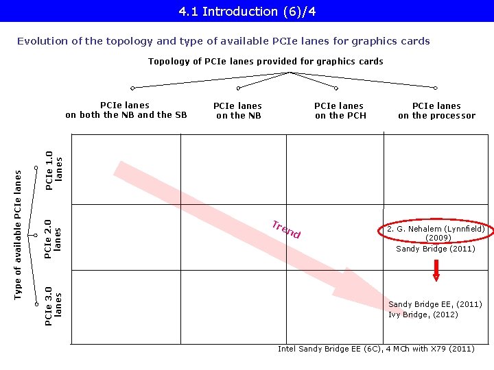
4. 1 Introduction (6)/4 Evolution of the topology and type of available PCIe lanes for graphics cards Topology of PCIe lanes provided for graphics cards PCIe lanes on the NB PCIe lanes on the PCH PCIe lanes on the processor PCIe 1. 0 lanes PCIe 2. 0 lanes PCIe 3. 0 lanes Type of available PCIe lanes on both the NB and the SB Tre n d 2. G. Nehalem (Lynnfield) (2009) Sandy Bridge (2011) Sandy Bridge EE, (2011) Ivy Bridge, (2012) Intel Sandy Bridge EE (6 C), 4 MCh with X 79 (2011)
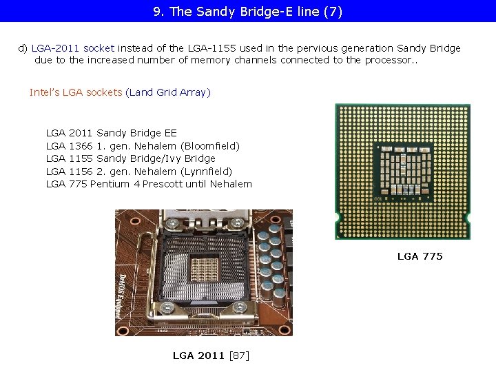
9. The Sandy Bridge-E line (7) d) LGA-2011 socket instead of the LGA-1155 used in the pervious generation Sandy Bridge due to the increased number of memory channels connected to the processor. . Intel’s LGA sockets (Land Grid Array) LGA LGA LGA 2011 Sandy Bridge EE 1366 1. gen. Nehalem (Bloomfield) 1155 Sandy Bridge/Ivy Bridge 1156 2. gen. Nehalem (Lynnfield) 775 Pentium 4 Prescott until Nehalem LGA 775 LGA 2011 [87]
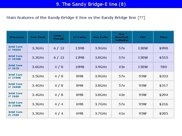
9. The Sandy Bridge-E line (8) Main features of the Sandy Bridge-E line vs the Sandy Bridge line [77] Core Clock Cores / Threads L 3 Cache Max Turbo Max Overclock Multiplier TDP Price Intel Core i 7 3960 X 3. 3 GHz 6 / 12 15 MB 3. 9 GHz 57 x 130 W $990 Intel Core i 7 3930 K 3. 2 GHz 6 / 12 12 MB 3. 8 GHz 57 x 130 W $555 Intel Core i 7 3820 3. 6 GHz 4 / 8 10 MB 3. 9 GHz 43 x 130 W TBD Intel Core i 7 2700 K 3. 5 GHz 4 / 8 8 MB 3. 9 GHz 57 x 95 W $332 Intel Core i 7 2600 K 3. 4 GHz 4 / 8 8 MB 3. 8 GHz 57 x 95 W $317 Intel Core i 7 2600 3. 4 GHz 4 / 8 8 MB 3. 8 GHz 42 x 95 W $294 Intel Core i 5 2500 K 3. 3 GHz 4 / 4 6 MB 3. 7 GHz 57 x 95 W $216 Intel Core i 5 2500 3. 3 GHz 4 / 4 6 MB 3. 7 GHz 41 x 95 W $205 Processor

10. The Ivy Bridge line
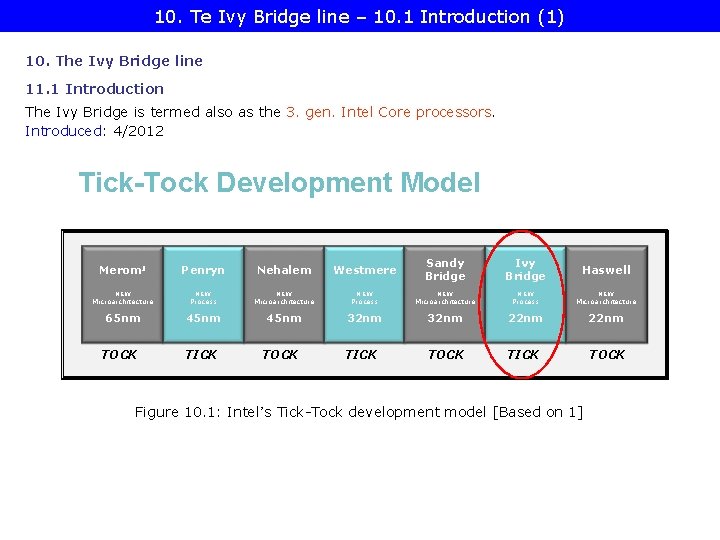
10. Te Ivy Bridge line – 10. 1 Introduction (1) 10. The Ivy Bridge line 11. 1 Introduction The Ivy Bridge is termed also as the 3. gen. Intel Core processors. Introduced: 4/2012 Tick-Tock Development Model Merom 1 NEW Penryn NEW Nehalem NEW Westmere NEW Sandy Bridge NEW Ivy Bridge NEW Haswell NEW Microarchitecture Process Microarchitecture 65 nm 45 nm 32 nm 22 nm TOCK TICK TOCK Figure 10. 1: Intel’s Tick-Tock development model [Based on 1]
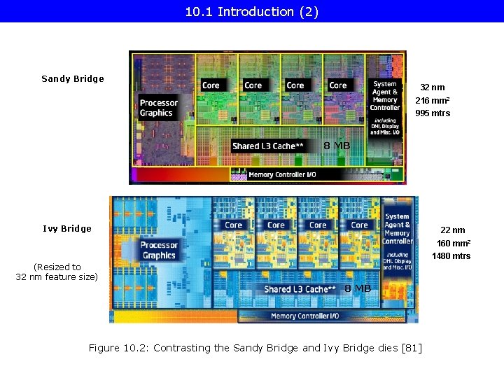
10. 1 Introduction (2) Sandy Bridge 32 nm 216 mm 2 995 mtrs 8 MB Ivy Bridge 22 nm 160 mm 2 1480 mtrs (Resized to 32 nm feature size) 8 MB Figure 10. 2: Contrasting the Sandy Bridge and Ivy Bridge dies [81]
![10. 1 Introduction (3) [84] 10. 1 Introduction (3) [84]](http://slidetodoc.com/presentation_image/922db7a576aee110ccfc0479cb511247/image-35.jpg)
10. 1 Introduction (3) [84]
![10. 1 Introduction (4) Major innovations of Ivy Bridge [80] 10. 1 Introduction (4) Major innovations of Ivy Bridge [80]](http://slidetodoc.com/presentation_image/922db7a576aee110ccfc0479cb511247/image-36.jpg)
10. 1 Introduction (4) Major innovations of Ivy Bridge [80]
11. 2 The new 22 nm tri-gate process technology (1) 11. 2 The new 22 nm tri-gate process technology [82]
![10. 2 The new 22 nm tri-gate process technology (2) [82] 10. 2 The new 22 nm tri-gate process technology (2) [82]](http://slidetodoc.com/presentation_image/922db7a576aee110ccfc0479cb511247/image-38.jpg)
10. 2 The new 22 nm tri-gate process technology (2) [82]
![10. 2 The new 22 nm tri-gate process technology (3) [82] 10. 2 The new 22 nm tri-gate process technology (3) [82]](http://slidetodoc.com/presentation_image/922db7a576aee110ccfc0479cb511247/image-39.jpg)
10. 2 The new 22 nm tri-gate process technology (3) [82]
![10. 2 The new 22 nm tri-gate process technology (4) [82] 10. 2 The new 22 nm tri-gate process technology (4) [82]](http://slidetodoc.com/presentation_image/922db7a576aee110ccfc0479cb511247/image-40.jpg)
10. 2 The new 22 nm tri-gate process technology (4) [82]
![10. 2 The new 22 nm tri-gate process technology (5) [82] 10. 2 The new 22 nm tri-gate process technology (5) [82]](http://slidetodoc.com/presentation_image/922db7a576aee110ccfc0479cb511247/image-41.jpg)
10. 2 The new 22 nm tri-gate process technology (5) [82]
![10. 2 The new 22 nm tri-gate process technology (6) [82] 10. 2 The new 22 nm tri-gate process technology (6) [82]](http://slidetodoc.com/presentation_image/922db7a576aee110ccfc0479cb511247/image-42.jpg)
10. 2 The new 22 nm tri-gate process technology (6) [82]
![10. 2 The new 22 nm tri-gate process technology (7) [82] 10. 2 The new 22 nm tri-gate process technology (7) [82]](http://slidetodoc.com/presentation_image/922db7a576aee110ccfc0479cb511247/image-43.jpg)
10. 2 The new 22 nm tri-gate process technology (7) [82]
![10. 2 The new 22 nm tri-gate process technology (8) [82] 10. 2 The new 22 nm tri-gate process technology (8) [82]](http://slidetodoc.com/presentation_image/922db7a576aee110ccfc0479cb511247/image-44.jpg)
10. 2 The new 22 nm tri-gate process technology (8) [82]
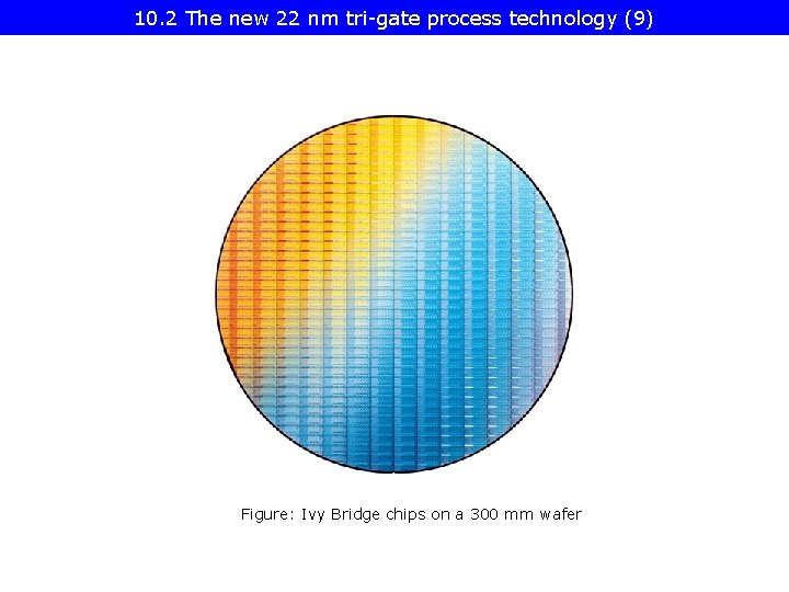
10. 2 The new 22 nm tri-gate process technology (9) Figure: Ivy Bridge chips on a 300 mm wafer
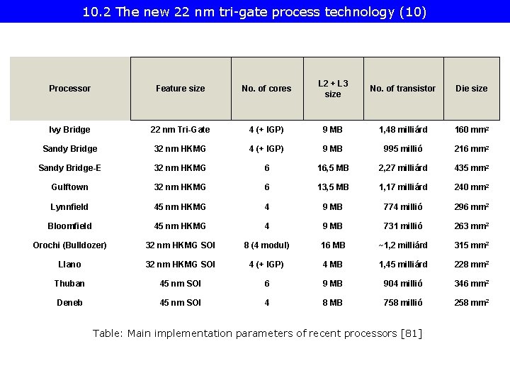
10. 2 The new 22 nm tri-gate process technology (10) Processor Feature size No. of cores L 2 + L 3 size No. of transistor Die size Ivy Bridge 22 nm Tri-Gate 4 (+ IGP) 9 MB 1, 48 milliárd 160 mm 2 Sandy Bridge 32 nm HKMG 4 (+ IGP) 9 MB 995 millió 216 mm 2 Sandy Bridge-E 32 nm HKMG 6 16, 5 MB 2, 27 milliárd 435 mm 2 Gulftown 32 nm HKMG 6 13, 5 MB 1, 17 milliárd 240 mm 2 Lynnfield 45 nm HKMG 4 9 MB 774 millió 296 mm 2 Bloomfield 45 nm HKMG 4 9 MB 731 millió 263 mm 2 Orochi (Bulldozer) 32 nm HKMG SOI 8 (4 modul) 16 MB ~1, 2 milliárd 315 mm 2 Llano 32 nm HKMG SOI 4 (+ IGP) 4 MB 1, 45 milliárd 228 mm 2 Thuban 45 nm SOI 6 9 MB 904 millió 346 mm 2 Deneb 45 nm SOI 4 8 MB 758 millió 258 mm 2 Table: Main implementation parameters of recent processors [81]
![10. 3 Supervisory Mode Execution Protection (SMEP) [83] 10. 3 Supervisory Mode Execution Protection (SMEP) [83]](http://slidetodoc.com/presentation_image/922db7a576aee110ccfc0479cb511247/image-47.jpg)
10. 3 Supervisory Mode Execution Protection (SMEP) [83]
![10. 4 System architecture (1) [81] 10. 4 System architecture (1) [81]](http://slidetodoc.com/presentation_image/922db7a576aee110ccfc0479cb511247/image-48.jpg)
10. 4 System architecture (1) [81]
![10. 4 System architecture (2)/1 [81] 10. 4 System architecture (2)/1 [81]](http://slidetodoc.com/presentation_image/922db7a576aee110ccfc0479cb511247/image-49.jpg)
10. 4 System architecture (2)/1 [81]
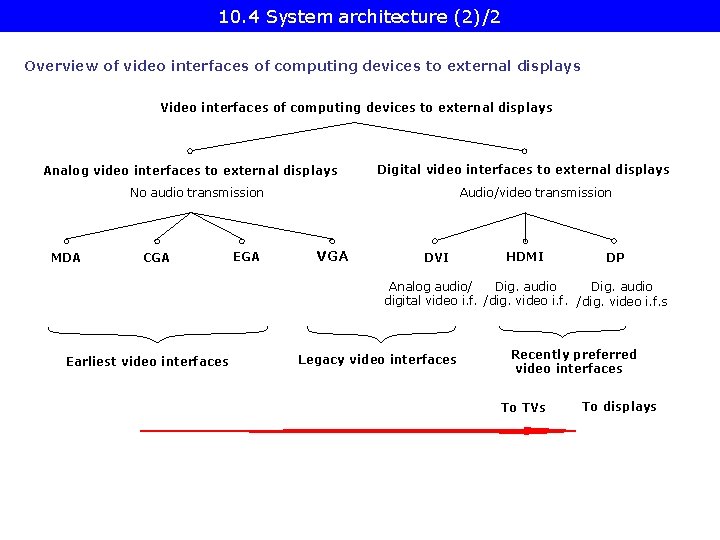
10. 4 System architecture (2)/2 Overview of video interfaces of computing devices to external displays Video interfaces of computing devices to external displays Analog video interfaces to external displays Digital video interfaces to external displays Audio/video transmission No audio transmission MDA CGA EGA VGA DVI HDMI DP Analog audio/ Dig. audio digital video i. f. /dig. video i. f. s Earliest video interfaces Legacy video interfaces Recently preferred video interfaces To TVs To displays
![10. 5 Performance (1) [81] Sandy Bridge EE Ivy Bridge Sandy Bridge EE Sandy 10. 5 Performance (1) [81] Sandy Bridge EE Ivy Bridge Sandy Bridge EE Sandy](http://slidetodoc.com/presentation_image/922db7a576aee110ccfc0479cb511247/image-51.jpg)
10. 5 Performance (1) [81] Sandy Bridge EE Ivy Bridge Sandy Bridge EE Sandy Bridge Bulldozer
![10. 5 Performance (2) [81] 10. 5 Performance (2) [81]](http://slidetodoc.com/presentation_image/922db7a576aee110ccfc0479cb511247/image-52.jpg)
10. 5 Performance (2) [81]

11. The Haswell line
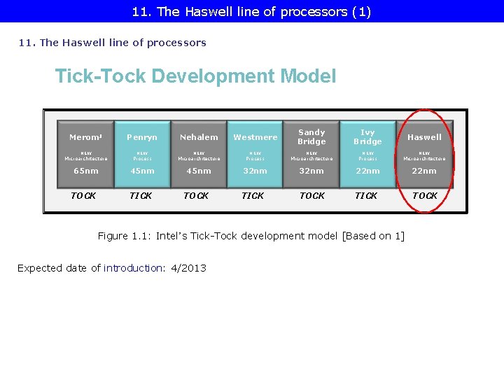
11. The Haswell line of processors (1) 11. The Haswell line of processors Tick-Tock Development Model Merom 1 NEW Penryn NEW Nehalem NEW Westmere NEW Sandy Bridge NEW Ivy Bridge NEW Haswell NEW Microarchitecture Process Microarchitecture 65 nm 45 nm 32 nm 22 nm TOCK TICK TOCK Figure 1. 1: Intel’s Tick-Tock development model [Based on 1] Expected date of introduction: 4/2013
![11. The Haswell line of processors (2) The Haswell die [85] 11. The Haswell line of processors (2) The Haswell die [85]](http://slidetodoc.com/presentation_image/922db7a576aee110ccfc0479cb511247/image-55.jpg)
11. The Haswell line of processors (2) The Haswell die [85]
![11. The Haswell line of processors (3) Haswell’s system architecture [86] 11. The Haswell line of processors (3) Haswell’s system architecture [86]](http://slidetodoc.com/presentation_image/922db7a576aee110ccfc0479cb511247/image-56.jpg)
11. The Haswell line of processors (3) Haswell’s system architecture [86]
![11. The Haswell line of processors (4) [80] 11. The Haswell line of processors (4) [80]](http://slidetodoc.com/presentation_image/922db7a576aee110ccfc0479cb511247/image-57.jpg)
11. The Haswell line of processors (4) [80]
![11. The Haswell line of processors (5) [80] 11. The Haswell line of processors (5) [80]](http://slidetodoc.com/presentation_image/922db7a576aee110ccfc0479cb511247/image-58.jpg)
11. The Haswell line of processors (5) [80]
![11. The Haswell line of processors (6)/1 [80] FMA: Fused Multiply-Add ( ax b+c) 11. The Haswell line of processors (6)/1 [80] FMA: Fused Multiply-Add ( ax b+c)](http://slidetodoc.com/presentation_image/922db7a576aee110ccfc0479cb511247/image-59.jpg)
11. The Haswell line of processors (6)/1 [80] FMA: Fused Multiply-Add ( ax b+c)
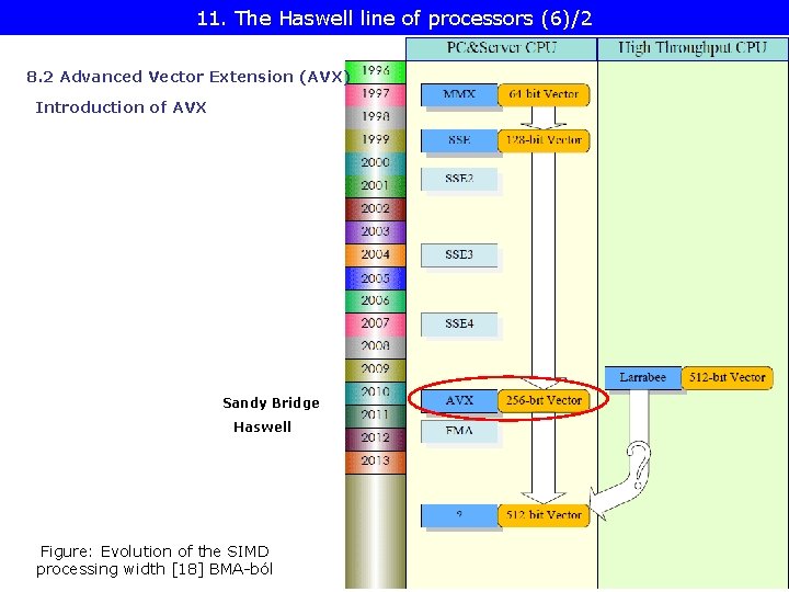
11. The Haswell line of processors (6)/2 8. 2 Advanced Vector Extension (AVX) Introduction of AVX Sandy Bridge Haswell Figure: Evolution of the SIMD processing width [18] BMA-ból
![11. The Haswell line of processors (7) [80] 11. The Haswell line of processors (7) [80]](http://slidetodoc.com/presentation_image/922db7a576aee110ccfc0479cb511247/image-61.jpg)
11. The Haswell line of processors (7) [80]

To 12 – Additional references
![[80]: Chappell R. , Toll B. , Singhal R. : Intel Next Generation Microarchitecture [80]: Chappell R. , Toll B. , Singhal R. : Intel Next Generation Microarchitecture](http://slidetodoc.com/presentation_image/922db7a576aee110ccfc0479cb511247/image-63.jpg)
[80]: Chappell R. , Toll B. , Singhal R. : Intel Next Generation Microarchitecture Codename Haswell: New Processor Innovations, IDF 2012 [81]: Olivera, A régóta várt Intel Ivy Bridge tesztje, Prohardware, 2012 -04 -13, http: //prohardver. hu/teszt/intel_ivy_bridge_teszt/az_ivy_bridge. html [82]: Bohr M. , Mistry K. : Intel’s Revolutionary 22 nm transistor technology, May 2011, http: //download. intel. com/newsroom/kits/22 nm/pdfs/22 nm-Details_Presentation. pdf [83]: George V. , Piazza T. , Jiang H. : Technology Insight: Intel Next Generation Microarchitecture Codename Ivy Bridge, IDF 2011 [84] 3 rd Generation Intel Core Processor Family Quad Core Launch Product Information, April 23, 2012 http: //download. intel. com/newsroom/kits/core/3 rdgen/pdfs/3 rd_Generation _Intel_Core_Product_Information. pdf [85] Ivy Bridge and Haswell die configurations (estimates included), Anandtech, 03 -21 -2012, http: //forums. anandtech. com/showthread. php? t=2234017 [86]: Piazza T. , Jiang H. , Hammerlund P. , Singhal R. : Technology Insight: Intel Next Generation Microarchitecture Codename Haswell, IDF 2012 SPCS 001 [87] Haynes D. : 2012 Socket Guide, Aug. 4 2012, http: //www. ocmodshop. com/cpu-socket-guide-2012/lga 2011/
- Slides: 63