Evolution of Implementation Technologies z Discrete devices relays
- Slides: 68

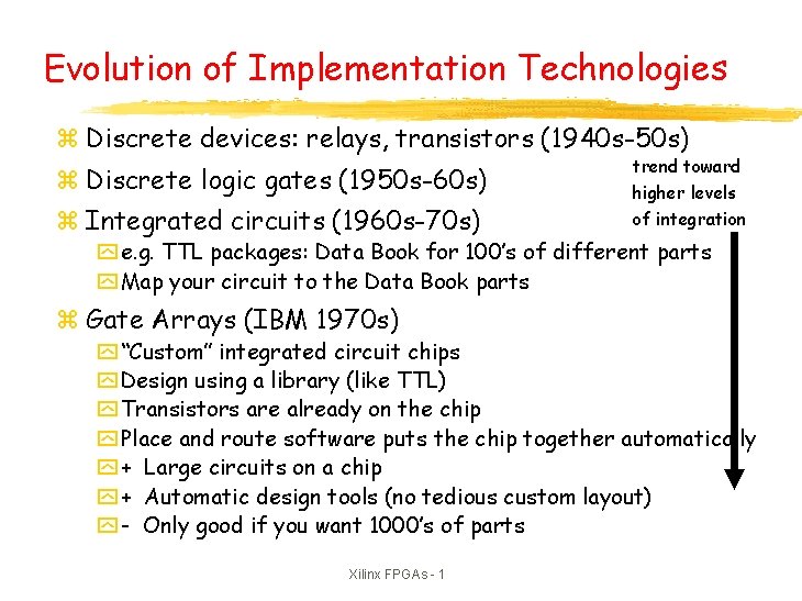
Evolution of Implementation Technologies z Discrete devices: relays, transistors (1940 s-50 s) z Discrete logic gates (1950 s-60 s) z Integrated circuits (1960 s-70 s) trend toward higher levels of integration y e. g. TTL packages: Data Book for 100’s of different parts y Map your circuit to the Data Book parts z Gate Arrays (IBM 1970 s) y “Custom” integrated circuit chips y Design using a library (like TTL) y Transistors are already on the chip y Place and route software puts the chip together automatically y + Large circuits on a chip y + Automatic design tools (no tedious custom layout) y - Only good if you want 1000’s of parts Xilinx FPGAs - 1

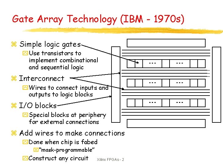
Gate Array Technology (IBM - 1970 s) z Simple logic gates y Use transistors to implement combinational and sequential logic z Interconnect y Wires to connect inputs and outputs to logic blocks z I/O blocks y Special blocks at periphery for external connections z Add wires to make connections y Done when chip is fabed x“mask-programmable” y Construct any circuit Xilinx FPGAs - 2

Programmable Logic z Disadvantages of the Data Book method y Constrained to parts in the Data Book y Parts are necessarily small and standard y Need to stock many different parts z Programmable logic y Use a single chip (or a small number of chips) y Program it for the circuit you want y No reason for the circuit to be small Xilinx FPGAs - 3

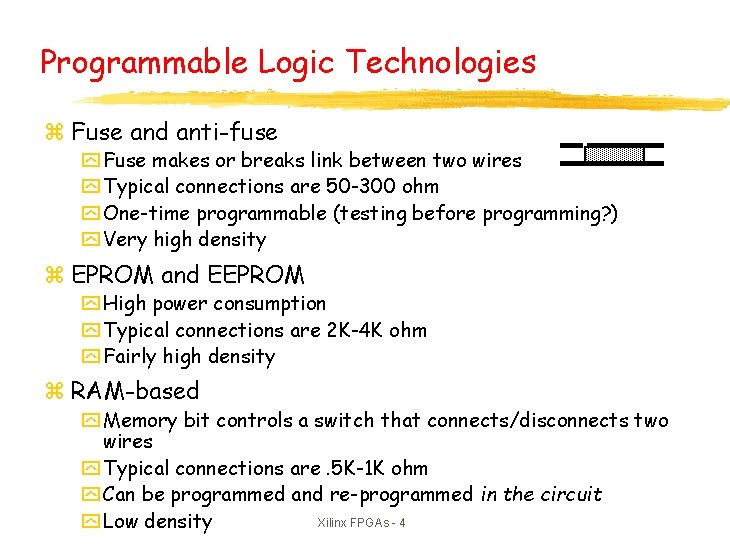
Programmable Logic Technologies z Fuse and anti-fuse y Fuse makes or breaks link between two wires y Typical connections are 50 -300 ohm y One-time programmable (testing before programming? ) y Very high density z EPROM and EEPROM y High power consumption y Typical connections are 2 K-4 K ohm y Fairly high density z RAM-based y Memory bit controls a switch that connects/disconnects two wires y Typical connections are. 5 K-1 K ohm y Can be programmed and re-programmed in the circuit Xilinx FPGAs - 4 y Low density

Programmable Logic z Program a connection y Connect two wires y Set a bit to 0 or 1 z Regular structures for two-level logic (1960 s-70 s) y All rely on two-level logic minimization y PROM connections - permanent y EPROM connections - erase with UV light y EEPROM connections - erase electrically y PROMs x. Program connections in the _______ plane y PLAs x. Program the connections in the ______ plane y PALs x. Program the connections in the ______ plane Xilinx FPGAs - 5

Making Large Programmable Logic Circuits z Alternative 1 : “CPLD” y Put a lot of PLDS on a chip y Add wires between them whose connections can be programmed y Use fuse/EEPROM technology z Alternative 2: “FPGA” y Emulate gate array technology y Hence Field Programmable Gate Array y You need: x. A way to implement logic gates x. A way to connect them together Xilinx FPGAs - 6

Field-Programmable Gate Arrays z PALs, PLAs = 10 - 100 Gate Equivalents z Field Programmable Gate Arrays = FPGAs y Altera MAX Family y Actel Programmable Gate Array y Xilinx Logical Cell Array z 100 - 1000(s) of Gate Equivalents! Xilinx FPGAs - 7

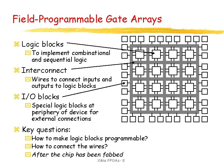
Field-Programmable Gate Arrays z Logic blocks y To implement combinational and sequential logic z Interconnect y Wires to connect inputs and outputs to logic blocks z I/O blocks y Special logic blocks at periphery of device for external connections z Key questions: y How to make logic blocks programmable? y How to connect the wires? y After the chip has been fabbed Xilinx FPGAs - 8

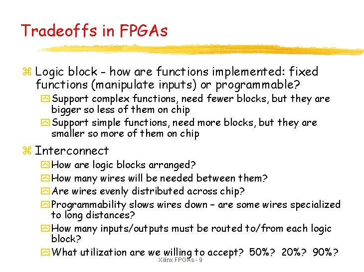
Tradeoffs in FPGAs z Logic block - how are functions implemented: fixed functions (manipulate inputs) or programmable? y Support complex functions, need fewer blocks, but they are bigger so less of them on chip y Support simple functions, need more blocks, but they are smaller so more of them on chip z Interconnect y How are logic blocks arranged? y How many wires will be needed between them? y Are wires evenly distributed across chip? y Programmability slows wires down – are some wires specialized to long distances? y How many inputs/outputs must be routed to/from each logic block? y What utilization are we willing to accept? 50%? 20%? 90%? Xilinx FPGAs - 9

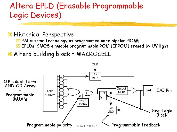
Altera EPLD (Erasable Programmable Logic Devices) z Historical Perspective y PALs: same technology as programmed once bipolar PROM y EPLDs: CMOS erasable programmable ROM (EPROM) erased by UV light z Altera building block = MACROCELL 8 Product Term AND-OR Array + Programmable MUX's I/O Pin Seq. Logic Block Programmable polarity Xilinx FPGAs - 10 Programmable feedback

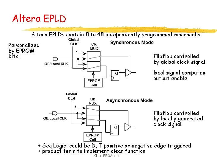
Altera EPLDs contain 8 to 48 independently programmed macrocells Personalized by EPROM bits: Flipflop controlled by global clock signal local signal computes output enable Flipflop controlled by locally generated clock signal + Seq Logic: could be D, T positive or negative edge triggered + product term to implement clear function Xilinx FPGAs - 11

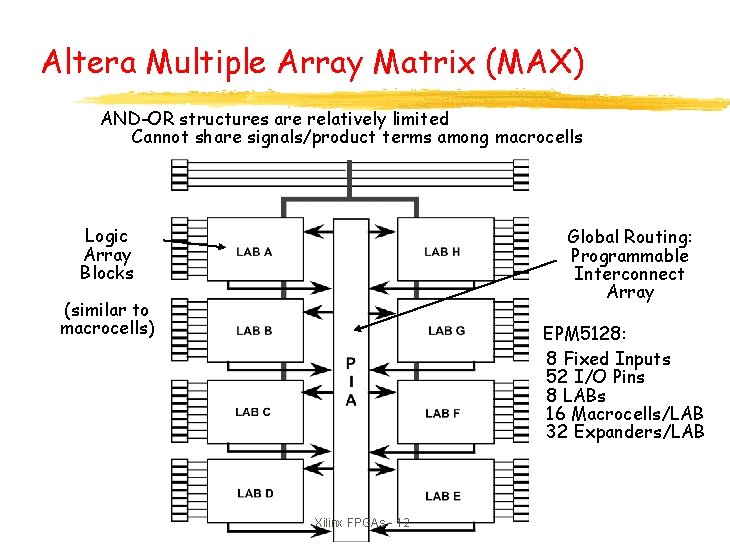
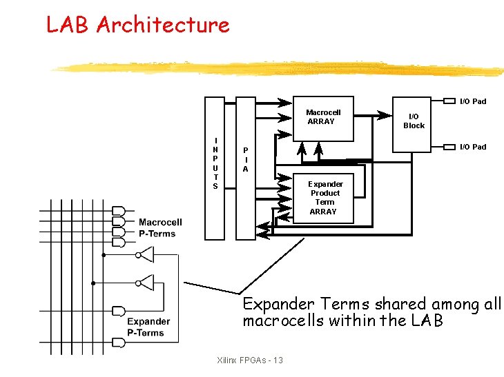
Altera Multiple Array Matrix (MAX) AND-OR structures are relatively limited Cannot share signals/product terms among macrocells Logic Array Blocks Global Routing: Programmable Interconnect Array (similar to macrocells) EPM 5128: 8 Fixed Inputs 52 I/O Pins 8 LABs 16 Macrocells/LAB 32 Expanders/LAB Xilinx FPGAs - 12

LAB Architecture I/O Pad Macrocell ARRAY I N P U T S I/O Block I/O Pad P I A Expander Product Term ARRAY Expander Terms shared among all macrocells within the LAB Xilinx FPGAs - 13

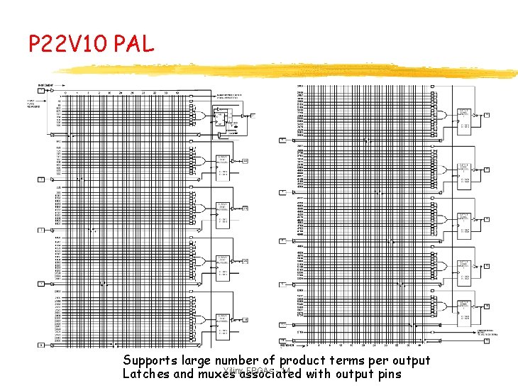
P 22 V 10 PAL Supports large number of product terms per output Xilinx FPGAs - 14 Latches and muxes associated with output pins

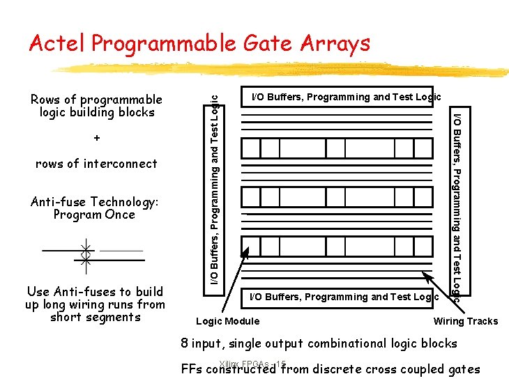
+ rows of interconnect Anti-fuse Technology: Program Once Use Anti-fuses to build up long wiring runs from short segments I/O Buffers, Programming and Test Logic Module I/O Buffers, Programming and Test Logic Rows of programmable logic building blocks I/O Buffers, Programming and Test Logic Actel Programmable Gate Arrays Wiring Tracks 8 input, single output combinational logic blocks Xilinx FPGAs - 15 FFs constructed from discrete cross coupled gates

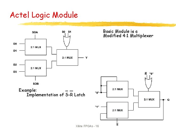
Actel Logic Module Basic Module is a Modified 4: 1 Multiplexer Example: Implementation of S-R Latch Xilinx FPGAs - 16

Actel Interconnection Fabric Xilinx FPGAs - 17

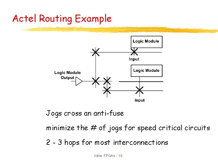
Actel Routing Example Jogs cross an anti-fuse minimize the # of jogs for speed critical circuits 2 - 3 hops for most interconnections Xilinx FPGAs - 18

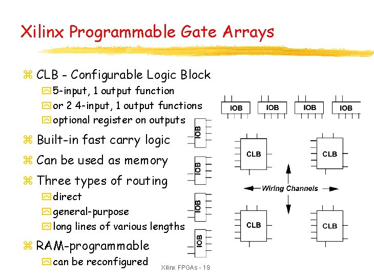
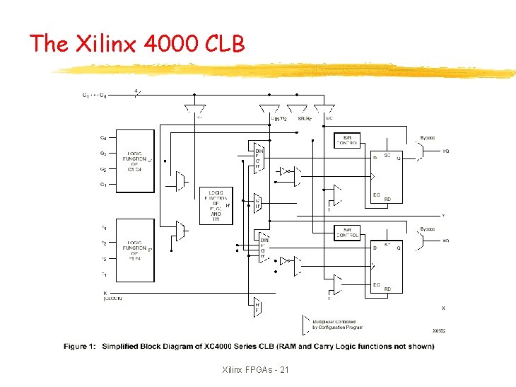
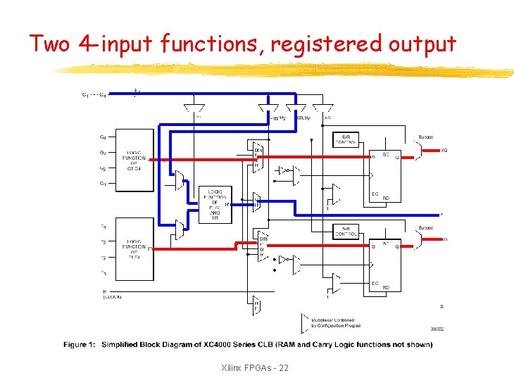
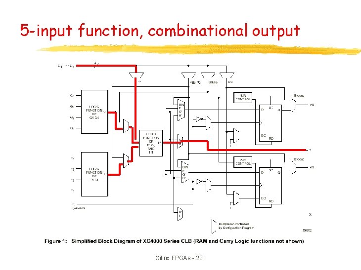
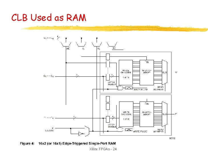
Xilinx Programmable Gate Arrays z CLB - Configurable Logic Block y 5 -input, 1 output function y or 2 4 -input, 1 output functions y optional register on outputs z Built-in fast carry logic z Can be used as memory z Three types of routing y direct y general-purpose y long lines of various lengths z RAM-programmable y can be reconfigured Xilinx FPGAs - 19

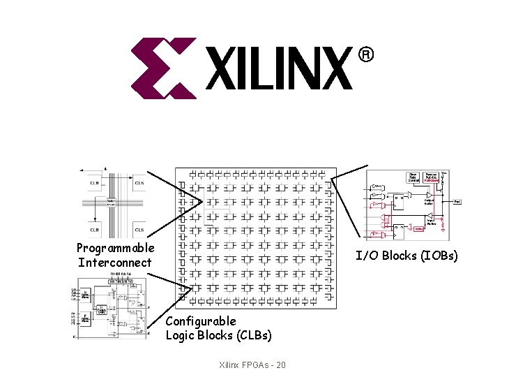
Programmable Interconnect I/O Blocks (IOBs) Configurable Logic Blocks (CLBs) Xilinx FPGAs - 20

The Xilinx 4000 CLB Xilinx FPGAs - 21

Two 4 -input functions, registered output Xilinx FPGAs - 22

5 -input function, combinational output Xilinx FPGAs - 23

CLB Used as RAM Xilinx FPGAs - 24

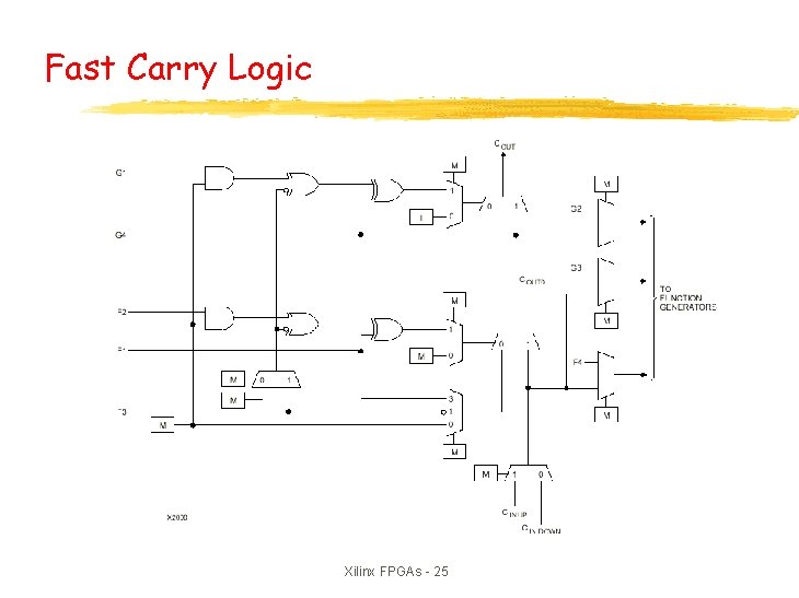
Fast Carry Logic Xilinx FPGAs - 25

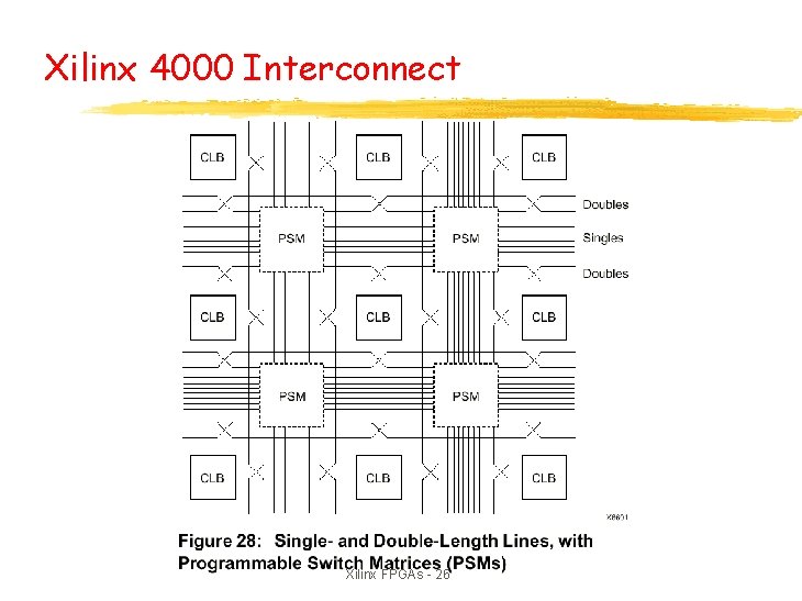
Xilinx 4000 Interconnect Xilinx FPGAs - 26

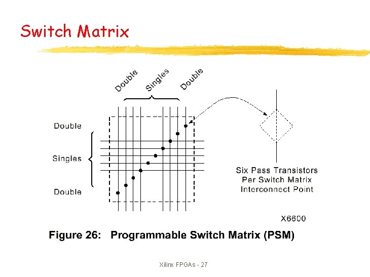
Switch Matrix Xilinx FPGAs - 27

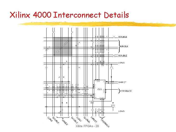
Xilinx 4000 Interconnect Details Xilinx FPGAs - 28

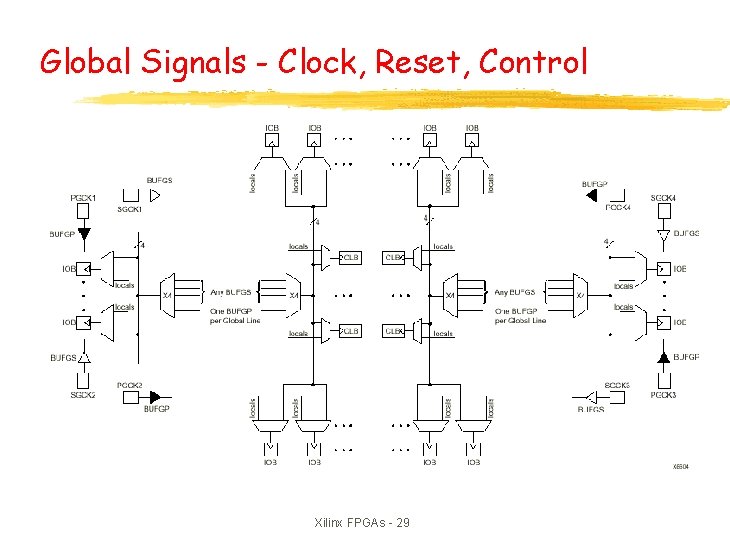
Global Signals - Clock, Reset, Control Xilinx FPGAs - 29

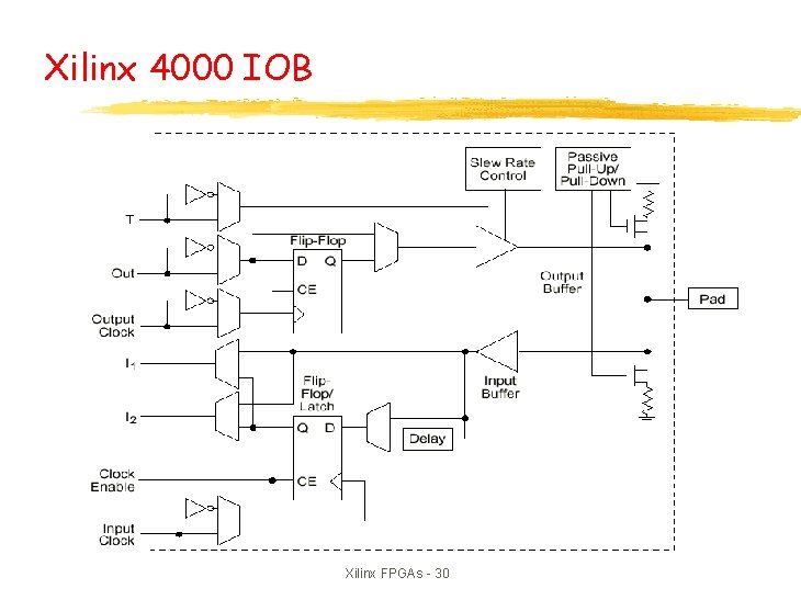
Xilinx 4000 IOB Xilinx FPGAs - 30

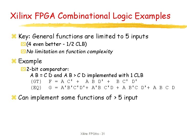
Xilinx FPGA Combinational Logic Examples z Key: General functions are limited to 5 inputs y (4 even better - 1/2 CLB) y No limitation on function complexity z Example y 2 -bit comparator: A B = C D and A B > C D implemented with 1 CLB (GT) F = A C' + A B D' + B C' D' (EQ) G = A'B'C'D'+ A'B C'D + A B'C D'+ A B C D z Can implement some functions of > 5 input Xilinx FPGAs - 31

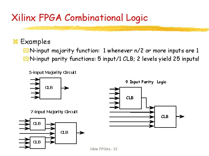
Xilinx FPGA Combinational Logic z Examples y N-input majority function: 1 whenever n/2 or more inputs are 1 y N-input parity functions: 5 input/1 CLB; 2 levels yield 25 inputs! 5 -input Majority Circuit 9 Input Parity Logic CLB 7 -input Majority Circuit CLB CLB Xilinx FPGAs - 32

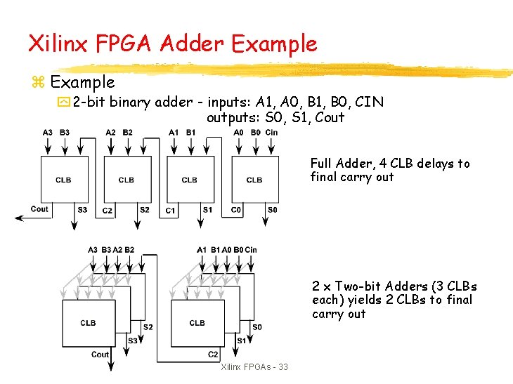
Xilinx FPGA Adder Example z Example y 2 -bit binary adder - inputs: A 1, A 0, B 1, B 0, CIN outputs: S 0, S 1, Cout Full Adder, 4 CLB delays to final carry out 2 x Two-bit Adders (3 CLBs each) yields 2 CLBs to final carry out Xilinx FPGAs - 33

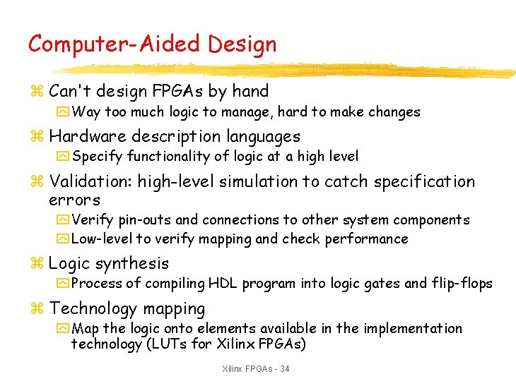
Computer-Aided Design z Can't design FPGAs by hand y Way too much logic to manage, hard to make changes z Hardware description languages y Specify functionality of logic at a high level z Validation: high-level simulation to catch specification errors y Verify pin-outs and connections to other system components y Low-level to verify mapping and check performance z Logic synthesis y Process of compiling HDL program into logic gates and flip-flops z Technology mapping y Map the logic onto elements available in the implementation technology (LUTs for Xilinx FPGAs) Xilinx FPGAs - 34

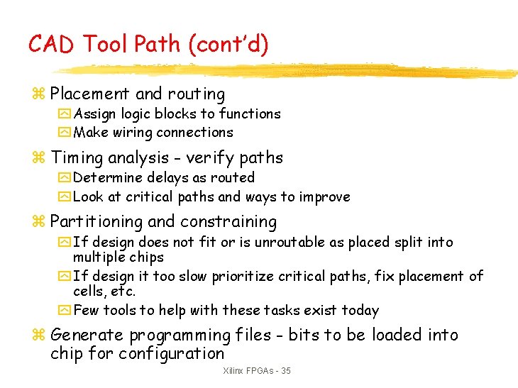
CAD Tool Path (cont’d) z Placement and routing y Assign logic blocks to functions y Make wiring connections z Timing analysis - verify paths y Determine delays as routed y Look at critical paths and ways to improve z Partitioning and constraining y If design does not fit or is unroutable as placed split into multiple chips y If design it too slow prioritize critical paths, fix placement of cells, etc. y Few tools to help with these tasks exist today z Generate programming files - bits to be loaded into chip for configuration Xilinx FPGAs - 35

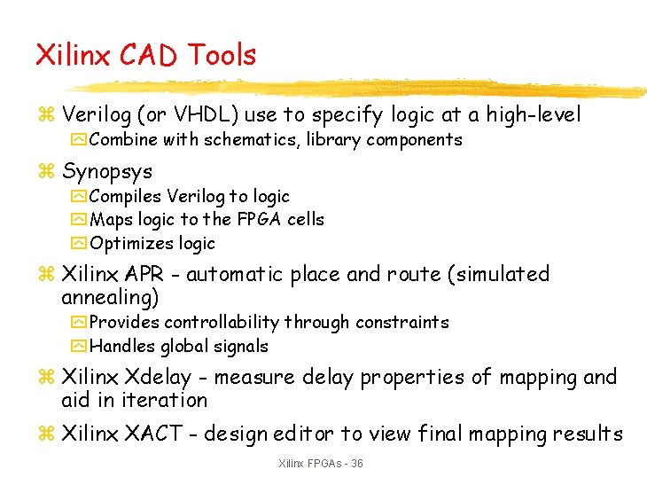
Xilinx CAD Tools z Verilog (or VHDL) use to specify logic at a high-level y Combine with schematics, library components z Synopsys y Compiles Verilog to logic y Maps logic to the FPGA cells y Optimizes logic z Xilinx APR - automatic place and route (simulated annealing) y Provides controllability through constraints y Handles global signals z Xilinx Xdelay - measure delay properties of mapping and aid in iteration z Xilinx XACT - design editor to view final mapping results Xilinx FPGAs - 36

Applications of FPGAs z Implementation of random logic y Easier changes at system-level (one device is modified) y Can eliminate need for full-custom chips z Prototyping y Ensemble of gate arrays used to emulate a circuit to be manufactured y Get more/better/faster debugging done than with simulation z Reconfigurable hardware y One hardware block used to implement more than one function y Functions must be mutually-exclusive in time y Can greatly reduce cost while enhancing flexibility y RAM-based only option z Special-purpose computation engines y Hardware dedicated to solving one problem (or class of problems) y Accelerators attached to general-purpose computers Xilinx FPGAs - 37

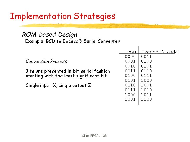
Implementation Strategies ROM-based Design Example: BCD to Excess 3 Serial Converter Conversion Process Bits are presented in bit serial fashion starting with the least significant bit Single input X, single output Z Xilinx FPGAs - 38 BCD 0000 0001 0010 0011 0100 0101 0110 0111 1000 1001 Excess 3 Code 0011 0100 0101 0110 0111 1000 1001 1010 1011 1100

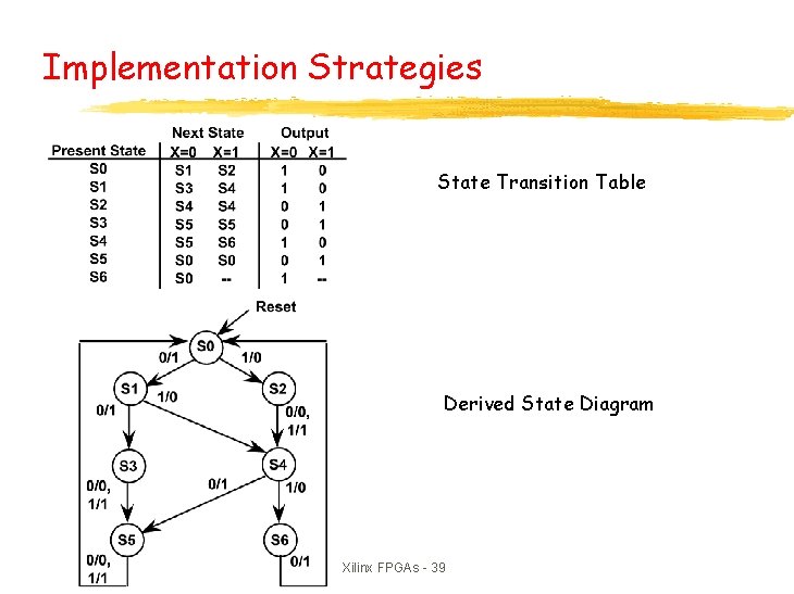
Implementation Strategies State Transition Table Derived State Diagram Xilinx FPGAs - 39

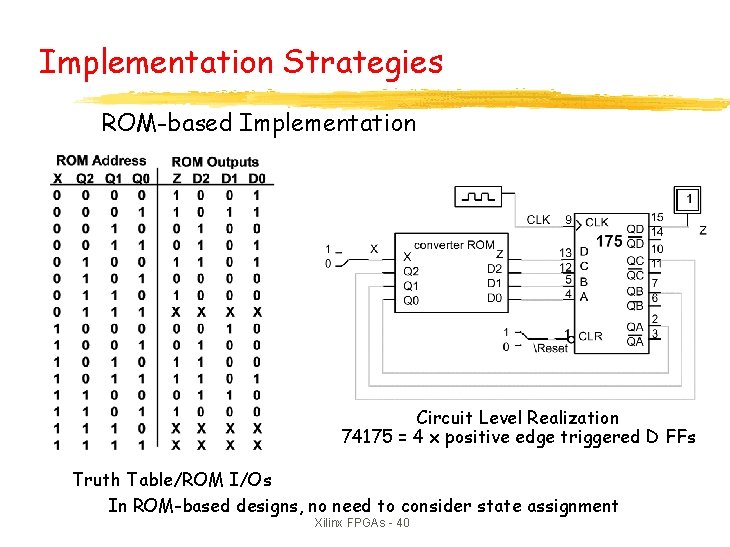
Implementation Strategies ROM-based Implementation Circuit Level Realization 74175 = 4 x positive edge triggered D FFs Truth Table/ROM I/Os In ROM-based designs, no need to consider state assignment Xilinx FPGAs - 40

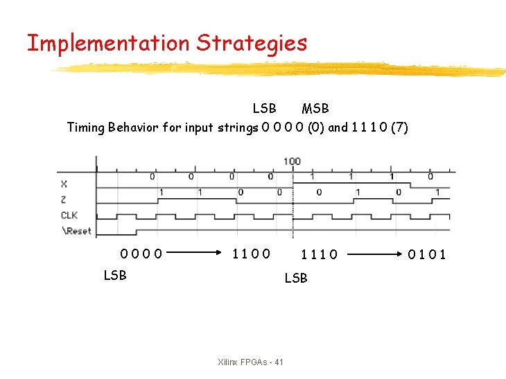
Implementation Strategies LSB MSB Timing Behavior for input strings 0 0 (0) and 1 1 1 0 (7) 0000 1100 LSB 1110 LSB Xilinx FPGAs - 41 0101

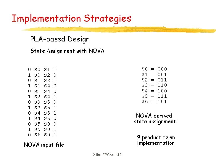
Implementation Strategies PLA-based Design State Assignment with NOVA 0 1 0 1 0 1 0 S 0 S 1 S 2 S 3 S 4 S 5 S 6 S 1 S 2 S 3 S 4 S 4 S 5 S 5 S 6 S 0 S 0 S 1 S 2 S 3 S 4 S 5 S 6 1 0 0 1 1 = = = = 000 001 011 110 100 111 101 NOVA derived state assignment 9 product term implementation NOVA input file Xilinx FPGAs - 42

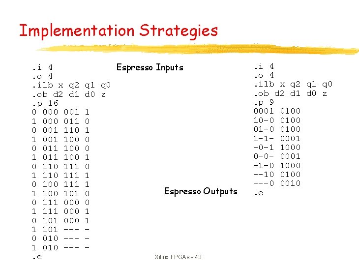
Implementation Strategies. i 4. o 4. ilb x q 2. ob d 2 d 1. p 16 0 001 1 000 011 0 001 110 1 001 100 0 011 100 1 011 100 0 111 1 110 111 0 100 111 1 100 101 0 111 000 1 111 000 0 101 000 1 101 --0 010 --1 010 --. e Espresso Inputs q 1 q 0 d 0 z 1 0 0 1 1 - Espresso Outputs Xilinx FPGAs - 43 . i 4. o 4. ilb x q 2 q 1 q 0. ob d 2 d 1 d 0 z. p 9 0001 0100 10 -0 0100 01 -0 0100 1 -1 - 0001 -0 -1 1000 0 -0 - 0001 -1 -0 1000 --10 0100 ---0 0010. e

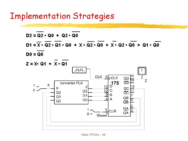
Implementation Strategies D 2 = Q 2 • Q 0 + Q 2 • Q 0 D 1 = X • Q 2 • Q 1 • Q 0 + X • Q 2 • Q 0 + Q 1 • Q 0 D 0 = Q 0 Z = X • Q 1 + X • Q 1 Xilinx FPGAs - 44

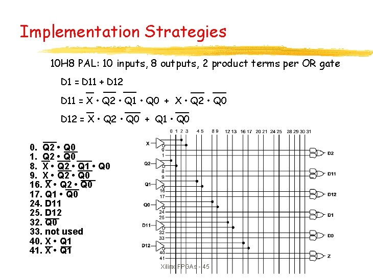
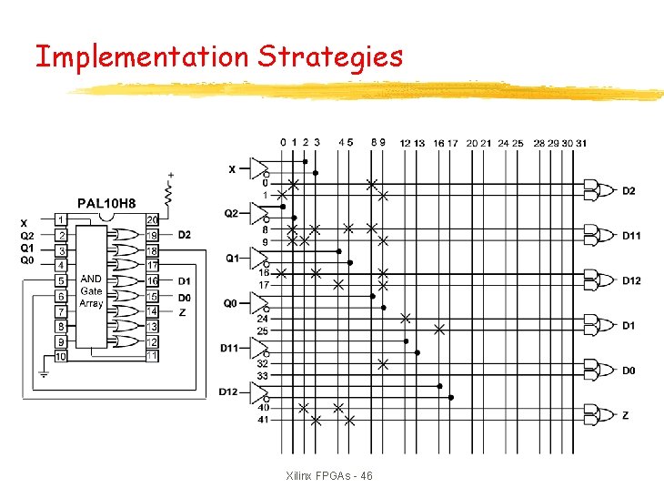
Implementation Strategies 10 H 8 PAL: 10 inputs, 8 outputs, 2 product terms per OR gate D 1 = D 11 + D 12 D 11 = X • Q 2 • Q 1 • Q 0 + X • Q 2 • Q 0 D 12 = X • Q 2 • Q 0 + Q 1 • Q 0 0. Q 2 • Q 0 1. Q 2 • Q 0 8. X • Q 2 • Q 1 • Q 0 9. X • Q 2 • Q 0 16. X • Q 2 • Q 0 17. Q 1 • Q 0 24. D 11 25. D 12 32. Q 0 33. not used 40. X • Q 1 41. X • Q 1 Xilinx FPGAs - 45

Implementation Strategies Xilinx FPGAs - 46

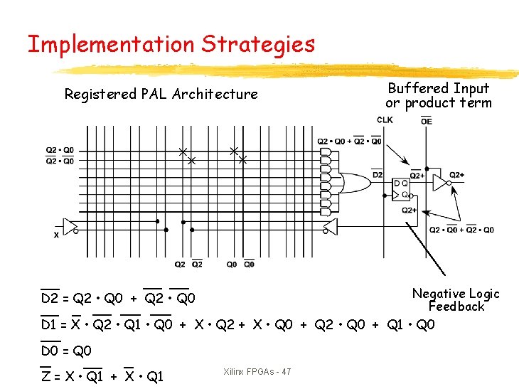
Implementation Strategies Registered PAL Architecture Buffered Input or product term Negative Logic Feedback D 1 = X • Q 2 • Q 1 • Q 0 + X • Q 2 + X • Q 0 + Q 2 • Q 0 + Q 1 • Q 0 D 2 = Q 2 • Q 0 + Q 2 • Q 0 D 0 = Q 0 Z = X • Q 1 + X • Q 1 Xilinx FPGAs - 47

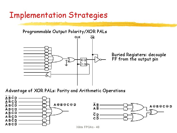
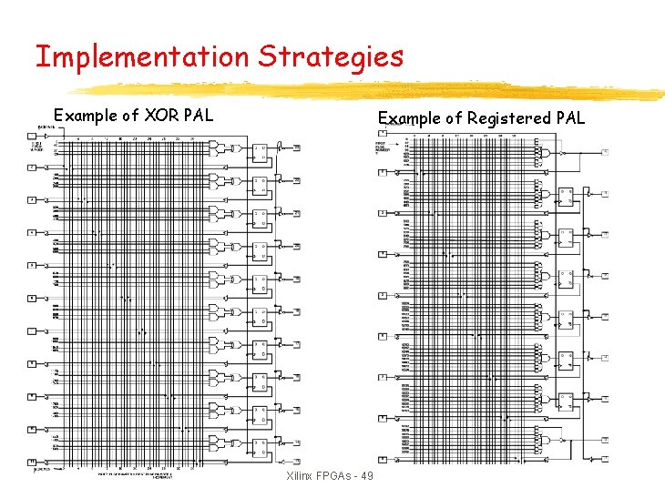
Implementation Strategies Programmable Output Polarity/XOR PALs Buried Registers: decouple FF from the output pin Advantage of XOR PALs: Parity and Arithmetic Operations Xilinx FPGAs - 48

Implementation Strategies Example of XOR PAL Example of Registered PAL Xilinx FPGAs - 49

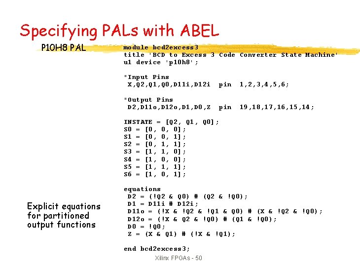
Specifying PALs with ABEL P 10 H 8 PAL module bcd 2 excess 3 title 'BCD to Excess 3 Code Converter State Machine' u 1 device 'p 10 h 8'; "Input Pins X, Q 2, Q 1, Q 0, D 11 i, D 12 i pin 1, 2, 3, 4, 5, 6; "Output Pins D 2, D 11 o, D 12 o, D 1, D 0, Z pin 19, 18, 17, 16, 15, 14; INSTATE = [Q 2, Q 1, Q 0]; S 0 = [0, 0, 0]; S 1 = [0, 0, 1]; S 2 = [0, 1, 1]; S 3 = [1, 1, 0]; S 4 = [1, 0, 0]; S 5 = [1, 1, 1]; S 6 = [1, 0, 1]; Explicit equations for partitioned output functions equations D 2 = (!Q 2 & Q 0) # (Q 2 & !Q 0); D 1 = D 11 i # D 12 i; D 11 o = (!X & !Q 2 & !Q 1 & Q 0) # (X & !Q 2 & !Q 0); D 12 o = (!X & Q 2 & !Q 0) # (Q 1 & !Q 0); D 0 = !Q 0; Z = (X & Q 1) # (!X & !Q 1); end bcd 2 excess 3; Xilinx FPGAs - 50

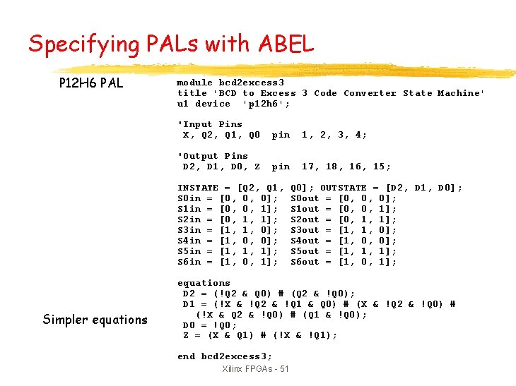
Specifying PALs with ABEL P 12 H 6 PAL module bcd 2 excess 3 title 'BCD to Excess 3 Code Converter State Machine' u 1 device 'p 12 h 6'; "Input Pins X, Q 2, Q 1, Q 0 pin 1, 2, 3, 4; "Output Pins D 2, D 1, D 0, Z pin 17, 18, 16, 15; INSTATE = [Q 2, Q 1, S 0 in = [0, 0, 0]; S 1 in = [0, 0, 1]; S 2 in = [0, 1, 1]; S 3 in = [1, 1, 0]; S 4 in = [1, 0, 0]; S 5 in = [1, 1, 1]; S 6 in = [1, 0, 1]; Simpler equations Q 0]; OUTSTATE = [D 2, D 1, D 0]; S 0 out = [0, 0, 0]; S 1 out = [0, 0, 1]; S 2 out = [0, 1, 1]; S 3 out = [1, 1, 0]; S 4 out = [1, 0, 0]; S 5 out = [1, 1, 1]; S 6 out = [1, 0, 1]; equations D 2 = (!Q 2 & Q 0) # (Q 2 & !Q 0); D 1 = (!X & !Q 2 & !Q 1 & Q 0) # (X & !Q 2 & !Q 0) # (!X & Q 2 & !Q 0) # (Q 1 & !Q 0); D 0 = !Q 0; Z = (X & Q 1) # (!X & !Q 1); end bcd 2 excess 3; Xilinx FPGAs - 51

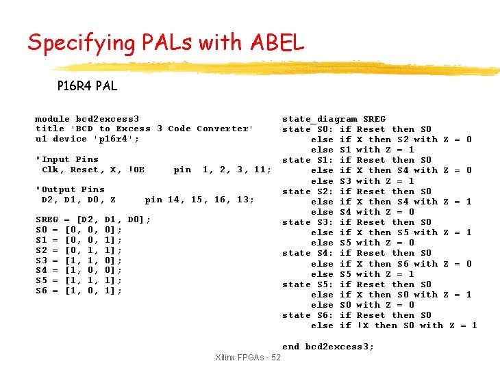
Specifying PALs with ABEL P 16 R 4 PAL module bcd 2 excess 3 title 'BCD to Excess 3 Code Converter' u 1 device 'p 16 r 4'; "Input Pins Clk, Reset, X, !OE "Output Pins D 2, D 1, D 0, Z SREG S 0 = S 1 = S 2 = S 3 = S 4 = S 5 = S 6 = = [D 2, [0, 0, [0, 1, [1, 0, [1, 1, [1, 0, pin 1, 2, 3, 11; pin 14, 15, 16, 13; D 1, D 0]; 0]; 1]; 1]; state_diagram SREG state S 0: if Reset then S 0 else if X then S 2 with Z = 0 else S 1 with Z = 1 state S 1: if Reset then S 0 else if X then S 4 with Z = 0 else S 3 with Z = 1 state S 2: if Reset then S 0 else if X then S 4 with Z = 1 else S 4 with Z = 0 state S 3: if Reset then S 0 else if X then S 5 with Z = 1 else S 5 with Z = 0 state S 4: if Reset then S 0 else if X then S 6 with Z = 0 else S 5 with Z = 1 state S 5: if Reset then S 0 else if X then S 0 with Z = 1 else S 0 with Z = 0 state S 6: if Reset then S 0 else if !X then S 0 with Z = 1 end bcd 2 excess 3; Xilinx FPGAs - 52

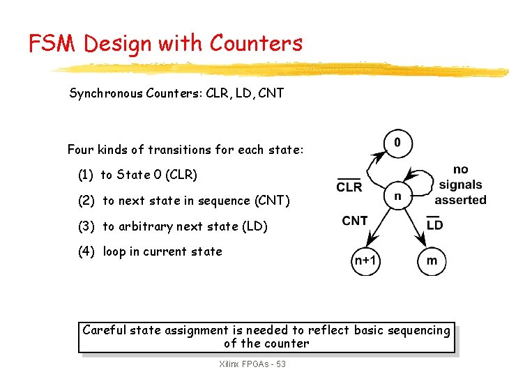
FSM Design with Counters Synchronous Counters: CLR, LD, CNT Four kinds of transitions for each state: (1) to State 0 (CLR) (2) to next state in sequence (CNT) (3) to arbitrary next state (LD) (4) loop in current state Careful state assignment is needed to reflect basic sequencing of the counter Xilinx FPGAs - 53

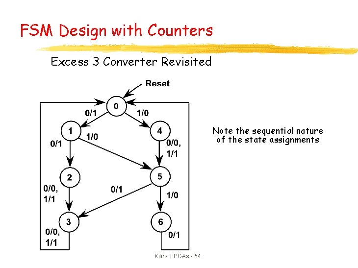
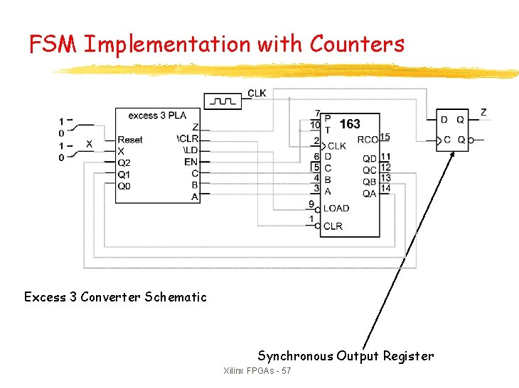
FSM Design with Counters Excess 3 Converter Revisited Note the sequential nature of the state assignments Xilinx FPGAs - 54

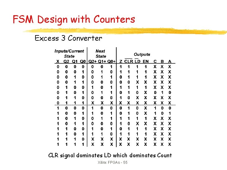
FSM Design with Counters Excess 3 Converter CLR signal dominates LD which dominates Count Xilinx FPGAs - 55

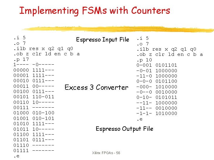
Implementing FSMs with Counters. i 5 Espresso Input File. i 5. o 7. ilb res x q 2 q 1 q 0. ob z clr ld en c b a. p 17. p 10 1 ---- -0 ----0 -001 0101101 00000 1111 ---0 -01 10000001 1111 ---11 -0 1000000 00010 0111 --0 -0 -0 0101100 00011 00 -----000 - 1010000 Excess 3 Converter 00100 0111 ---0 --0 0010000 00101 110 -011 0 -10 - 0101011 00110 10 ------11 - 1000000 00111 -------11 -- 0010000 010 -100 -1 -1 - 1010000 01001 010 -101. e 01010 1111 --01011 10 ----Espresso Output File 01100 1111 --01101 0111 --01110 ------01111 ------Xilinx FPGAs - 56. e

FSM Implementation with Counters Excess 3 Converter Schematic Synchronous Output Register Xilinx FPGAs - 57

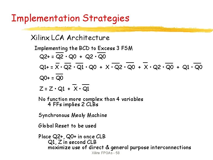
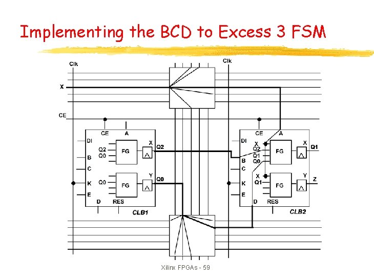
Implementation Strategies Xilinx LCA Architecture Implementing the BCD to Excess 3 FSM Q 2+ = Q 2 • Q 0 + Q 2 • Q 0 Q 1+ = X • Q 2 • Q 1 • Q 0 + X • Q 2 • Q 0 + Q 1 • Q 0+ = Q 0 Z = Z • Q 1 + X • Q 1 No function more complex than 4 variables 4 FFs implies 2 CLBs Synchronous Mealy Machine Global Reset to be used Place Q 2+, Q 0+ in once CLB Q 1, Z in second CLB maximize use of direct & general purpose interconnections Xilinx FPGAs - 58

Implementing the BCD to Excess 3 FSM Xilinx FPGAs - 59

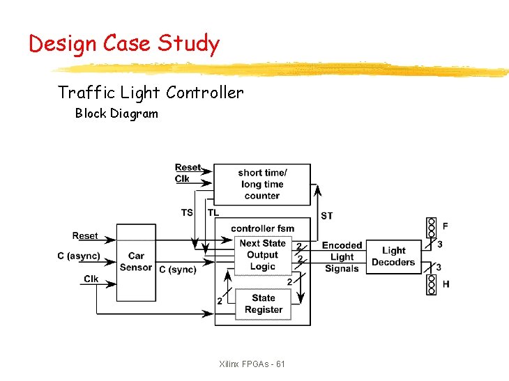
Design Case Study Traffic Light Controller Decomposition into primitive subsystems • Controller FSM next state/output functions state register • Short time/long time interval counter • Car Sensor • Output Decoders and Traffic Lights Xilinx FPGAs - 60

Design Case Study Traffic Light Controller Block Diagram Xilinx FPGAs - 61

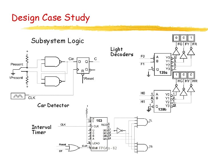
Design Case Study Subsystem Logic Light Decoders Car Detector Interval Timer Xilinx FPGAs - 62

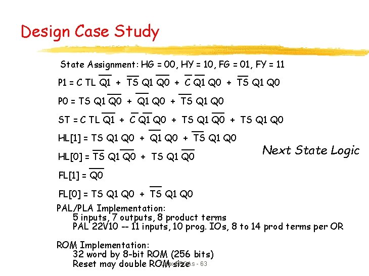
Design Case Study State Assignment: HG = 00, HY = 10, FG = 01, FY = 11 P 1 = C TL Q 1 + TS Q 1 Q 0 + C Q 1 Q 0 + TS Q 1 Q 0 P 0 = TS Q 1 Q 0 + TS Q 1 Q 0 ST = C TL Q 1 + C Q 1 Q 0 + TS Q 1 Q 0 HL[1] = TS Q 1 Q 0 + TS Q 1 Q 0 HL[0] = TS Q 1 Q 0 + TS Q 1 Q 0 Next State Logic FL[1] = Q 0 FL[0] = TS Q 1 Q 0 + TS Q 1 Q 0 PAL/PLA Implementation: 5 inputs, 7 outputs, 8 product terms PAL 22 V 10 -- 11 inputs, 10 prog. IOs, 8 to 14 prod terms per OR ROM Implementation: 32 word by 8 -bit ROM (256 bits) Xilinxsize FPGAs - 63 Reset may double ROM

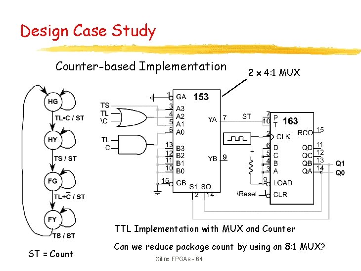
Design Case Study Counter-based Implementation 2 x 4: 1 MUX TTL Implementation with MUX and Counter ST = Count Can we reduce package count by using an 8: 1 MUX? Xilinx FPGAs - 64

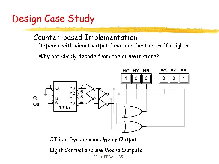
Design Case Study Counter-based Implementation Dispense with direct output functions for the traffic lights Why not simply decode from the current state? ST is a Synchronous Mealy Output Light Controllers are Moore Outputs Xilinx FPGAs - 65

Design Case Study LCA-Based Implementation Discrete Gate Method: None of the functions exceed 5 variables P 1, ST are 5 variable (1 CLB each) P 0, HL 1, HL 0, FL 0 are 3 variable (1/2 CLB each) FL 1 is 1 variable (1/2 CLB) 4 1/2 CLBs total! Xilinx FPGAs - 66

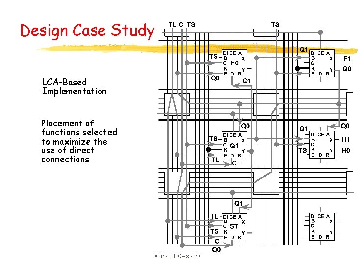
Design Case Study LCA-Based Implementation Placement of functions selected to maximize the use of direct connections Xilinx FPGAs - 67

Design Case Study LCA-Based Implementation Counter/Multiplexer Method: 4: 1 MUX, 2 Bit Upcounter MUX: six variables (4 data, 2 control) but this is the kind of 6 variable function that can be implemented in 1 CLB! 2 nd CLB to implement TL • C and TL + C' But note that ST/Cnt is really a function of TL, C, TS, Q 1, Q 0 1 CLB to implement this function of 5 variables! 2 Bit Counter: 2 functions of 3 variables (2 bit state + count) Also implemented in one CLB Traffic light decoders: functions of 2 variables (Q 1, Q 0) 2 per CLB = 3 CLB for the six lights Total count = 5 CLBs Xilinx FPGAs - 68