Evaluating the Raw microprocessor Michael Bedford Taylor n

Evaluating the Raw microprocessor Michael Bedford Taylor n Raw Architecture Group n Computer Science and AI Laboratory Massachusetts Institute of Technology

Evaluating the Raw microprocessor n n Brief Overview of Raw Architecture Avenues of Evaluation Empirical - Comparison with P 3 Analytical - Modeling Large scale ILP Experiential - Experimental Systems

The Raw Architecture Divide the silicon into an array of identical, programmable tiles. (A signal can get through a small amount of logic and to the next tile in one cycle. )

Raw Architecture Compute Processor Routers On-chip networks

Raw Architecture Compute Processor Routers On-chip networks

Inside the compute processor – networks are integrated directly into the bypass paths r 24 r 25 r 26 r 27 Input FIFOs from Static Router E M 1 A IF D Output FIFOs to Static Router RF F M 2 TL P TV U F 4 WB

Raw’s bypass-integrated on-chip networks serve as a Scalar Operand Network, or SON. Multiple Raw tiles Program graph seed. 0=seed pval 1=seed. 0*3. 0 v 1. 2=v 1 pval 1=seed. 0*3. 0 v 2. 4=v 2 pval 5=seed. 0*6. 0 pval 4=pval 5+2. 0 pval 5=seed. 0*6. 0 pval 0=pval 1+2. 0 tmp 0. 1=pval 0/2. 0 pval 2=seed. 0*v 1. 2 pval 0=pval 1+2. 0 pval 3=seed. o*v 2. 4 pval 4=pval 5+2. 0 tmp 1. 3=pval 2+2. 0 tmp 3. 6=pval 4/3. 0 tmp 3=tmp 3. 6 tmp 0. 1=pval 0/2. 0 tmp 2. 5=pval 3+2. 0 tmp 3. 6=pval 4/3. 0 tmp 1=tmp 1. 3 tmp 0=tmp 0. 1 tmp 2=tmp 2. 5 pval 7=tmp 1. 3+tmp 2. 5 v 3. 10=tmp 3. 6 -v 2. 7 tmp 0=tmp 0. 1 v 3=v 3. 10 tmp 3=tmp 3. 6 pval 6=tmp 1. 3 -tmp 2. 5 v 1. 8=pval 7*3. 0 v 1. 2=v 1 v 2. 4=v 2 pval 2=seed. 0*v 1. 2 pval 3=seed. o*v 2. 4 tmp 1. 3=pval 2+2. 0 tmp 2. 5=pval 3+2. 0 v 2. 7=pval 6*5. 0 v 0. 9=tmp 0. 1 -v 1. 8 v 1=v 1. 8 v 0=v 0. 9 v 3. 10=tmp 3. 6 -v 2. 7 v 2=v 2. 7 v 3=v 3. 10 tmp 1=tmp 1. 3 pval 7=tmp 1. 3+tmp 2. 5 v 1. 8=pval 7*3. 0 v 0. 9=tmp 0. 1 -v 1. 8 v 1=v 1. 8 v 0=v 0. 9 tmp 2=tmp 2. 5 pval 6=tmp 1. 3 -tmp 2. 5 v 2. 7=pval 6*5. 0 v 2=v 2. 7

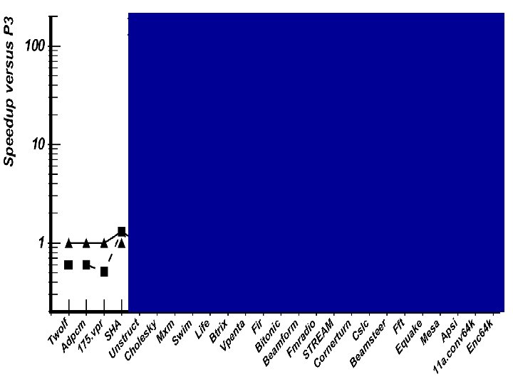
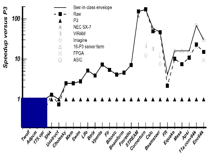
Empirical Evaluation Comparison to P 3 Parameter Litho Process Metal Layers FO 1 Delay Dielectric k Raw (IBM ASIC) 180 nm CMOS 7 SF Cu 6 23 ps 4. 1 P 3 (Intel) 180 nm P 858 Al 6 11 ps 3. 55 Design Style Initial Freq Die Area Standard Cell 425 MHz 331 mm 2 Full custom 500 -733 MHz 106 mm 2
. (See HPCA 2003 and future. )")
Analytical Evaluation Scalar Operand Network Research (SONs). (See HPCA 2003 and future. )

Scalar Operand Network The network and the associated algorithms that are responsible for matching operands and operations In space.

SON Performance Metric: 5 -tuple conventional distributed multiprocessor <3, 15, 2, 1, 12> Superscalar (not scalable) < 0, 0, 0>

Raw: a new point in the region. conventional distributed multiprocessor <3, 15, 2, 1, 12> Raw SON < 0, 1, 1, 1, 0> Superscalar SON (not scalable) < 0, 0, 0>

Impact of Receive Occupancy, 64 tiles, i. e. , <0, 1, 1, 1, n>
 Systems Online or in Pipeline")
Experiential Evaluation (i. e. , Real Hardware, Real Systems) Systems Online or in Pipeline Workstation Microphone Array Fabric System (Software Radio on Raw) (IP Routing on Raw)

Raw Chip Specifications IBM SA 27 E Process 180 nm, 6 -metal copper ASIC process 16 Tile RAW Processor 18. 23 mm x 18. 23 mm 1657 pin CCGA package 1152 HSTL signal pins Clock and Power 420 MHz (actual) 10 watts (power save mode) 18 watts typical 35 watts max

Raw Motherboard . . twenty-eight 32 -bit buses connecting Raw Chip to I/O and Memory System

2 Microphone Board 2 Microphones 1 A-to-D 1 CPLD 2 Connectors

1020 Element Microphone Array

Fabric System Architecture n n Design: two distinct board types Board 1: Quad Raw Board 2: I/O & Memory Board Replicate and connect

Summary
- Slides: 22