ETE 204 Digital Electronics Electrical and Timing Characteristics
- Slides: 28

ETE 204 – Digital Electronics Electrical and Timing Characteristics of Standard Logic Gates [Lecture: 3] Instructor: Sajib Roy Lecturer, ETE, ULAB

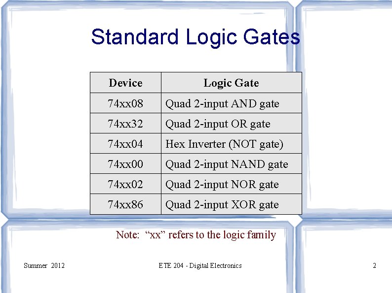
Standard Logic Gates Device Logic Gate 74 xx 08 Quad 2 -input AND gate 74 xx 32 Quad 2 -input OR gate 74 xx 04 Hex Inverter (NOT gate) 74 xx 00 Quad 2 -input NAND gate 74 xx 02 Quad 2 -input NOR gate 74 xx 86 Quad 2 -input XOR gate Note: “xx” refers to the logic family Summer 2012 ETE 204 - Digital Electronics 2

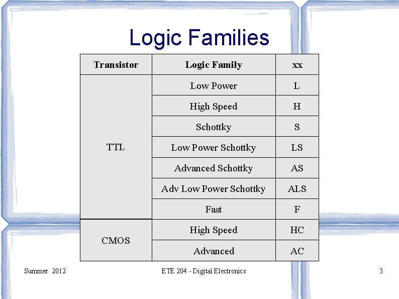
Logic Families Transistor TTL CMOS Summer 2012 Logic Family xx Low Power L High Speed H Schottky S Low Power Schottky LS Advanced Schottky AS Adv Low Power Schottky ALS Fast F High Speed HC Advanced AC ETE 204 - Digital Electronics 3

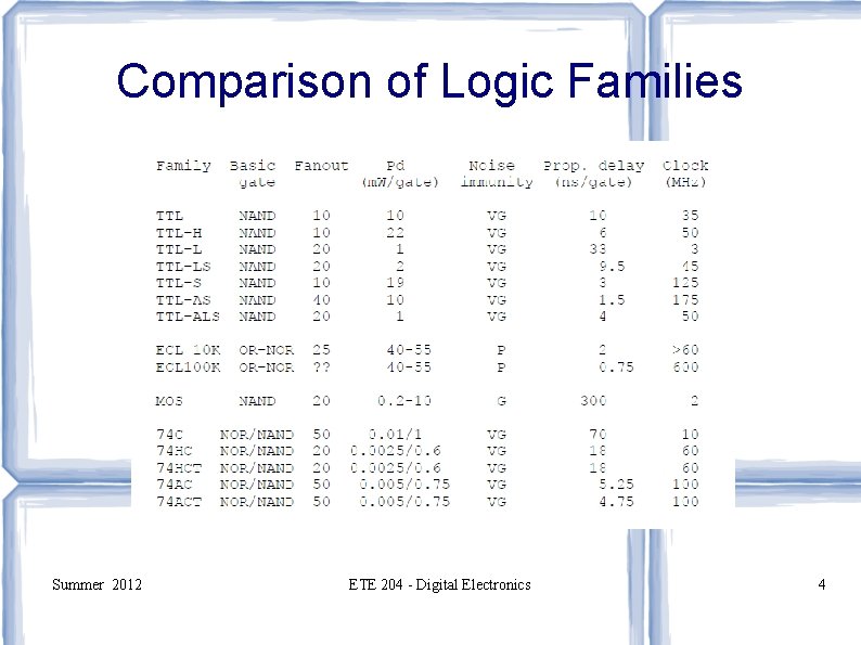
Comparison of Logic Families Summer 2012 ETE 204 - Digital Electronics 4

Example: 74 LS 08 (see data sheet for 74 LS 08) Summer 2012 ETE 204 - Digital Electronics 5

Example: 74 HC 08 (see data sheet for 74 HC 08) Summer 2012 ETE 204 - Digital Electronics 6

Basic Electrical Characteristics Summer 2012 ETE 204 - Digital Electronics 7

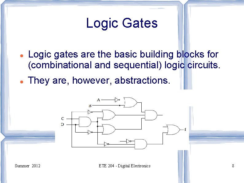
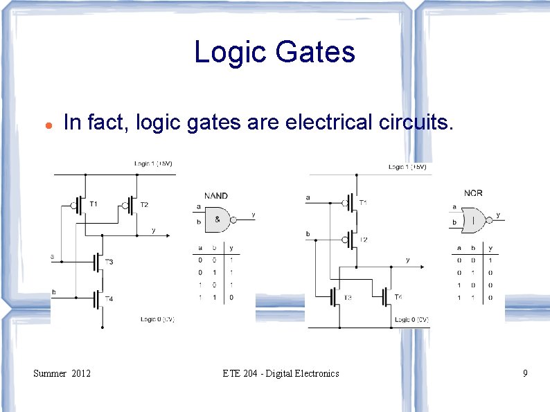
Logic Gates Logic gates are the basic building blocks for (combinational and sequential) logic circuits. They are, however, abstractions. Summer 2012 ETE 204 - Digital Electronics 8

Logic Gates In fact, logic gates are electrical circuits. Summer 2012 ETE 204 - Digital Electronics 9

Logic Gates As such, the logic levels must be represented using an electrical characteristic. Most technologies use voltages to represent the logic levels. TTL CMOS Some, but very few, technologies use currents to represent the logic levels. Summer 2012 ETE 204 - Digital Electronics 10

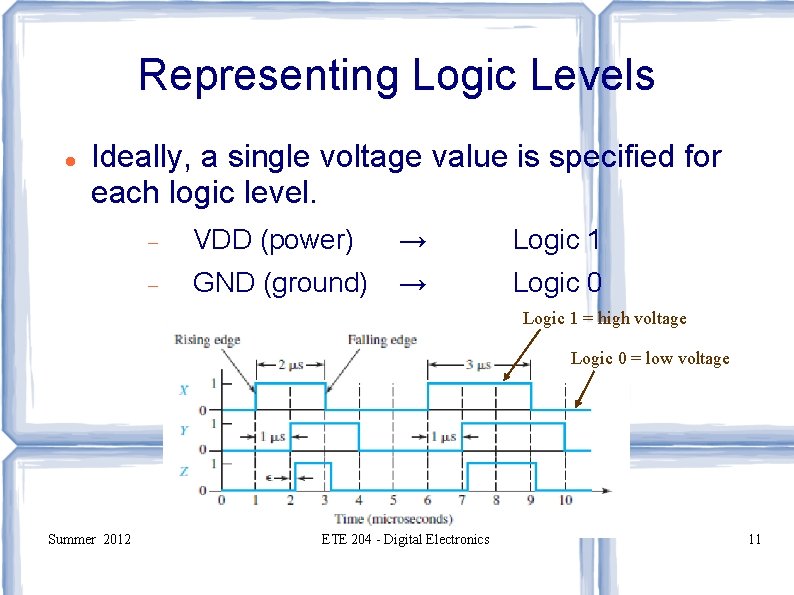
Representing Logic Levels Ideally, a single voltage value is specified for each logic level. VDD (power) → Logic 1 GND (ground) → Logic 0 Logic 1 = high voltage Logic 0 = low voltage Summer 2012 ETE 204 - Digital Electronics 11

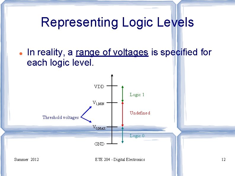
Representing Logic Levels In reality, a range of voltages is specified for each logic level. VDD Logic 1 V 1, MIN Undefined Threshold voltages V 0, MAX Logic 0 GND Summer 2012 ETE 204 - Digital Electronics 12

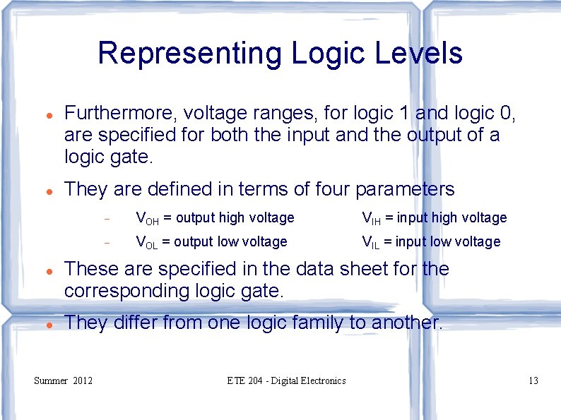
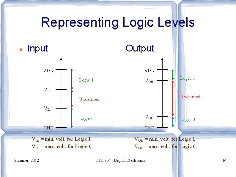
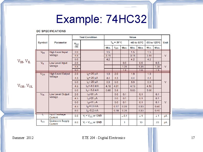
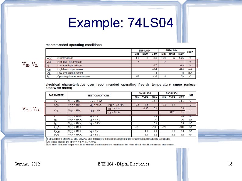
Representing Logic Levels Furthermore, voltage ranges, for logic 1 and logic 0, are specified for both the input and the output of a logic gate. They are defined in terms of four parameters VOH = output high voltage VIH = input high voltage VOL = output low voltage VIL = input low voltage These are specified in the data sheet for the corresponding logic gate. They differ from one logic family to another. Summer 2012 ETE 204 - Digital Electronics 13

Representing Logic Levels Input Output VDD Logic 1 VOH Logic 1 VIH Undefined VIL Logic 0 GND VIH = min. volt. for Logic 1 VIL = max. volt. for Logic 0 Summer 2012 VOL Logic 0 GND VOH = min. volt. for Logic 1 VOL = max. volt. for Logic 0 ETE 204 - Digital Electronics 14

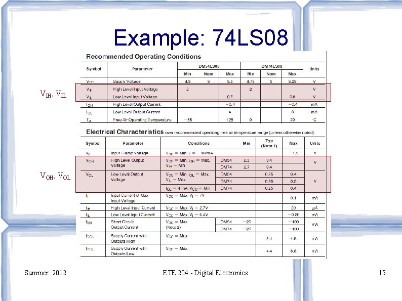
Example: 74 LS 08 VIH, VIL VOH, VOL Summer 2012 ETE 204 - Digital Electronics 15

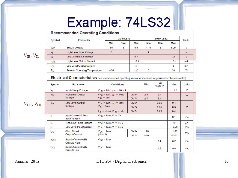
Example: 74 LS 32 VIH, VIL VOH, VOL Summer 2012 ETE 204 - Digital Electronics 16

Example: 74 HC 32 VIH, VIL VOH, VOL Summer 2012 ETE 204 - Digital Electronics 17

Example: 74 LS 04 VIH, VIL VOH, VOL Summer 2012 ETE 204 - Digital Electronics 18

Basic Timing Characteristics Summer 2012 ETE 204 - Digital Electronics 19

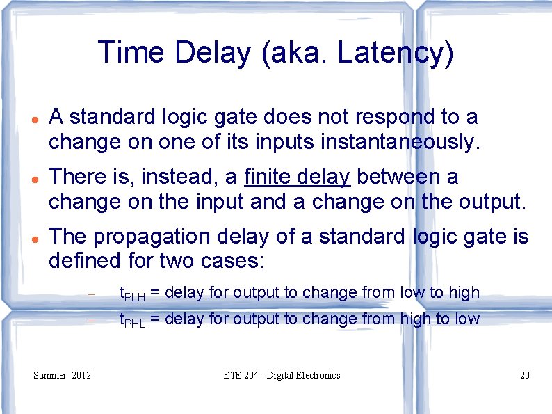
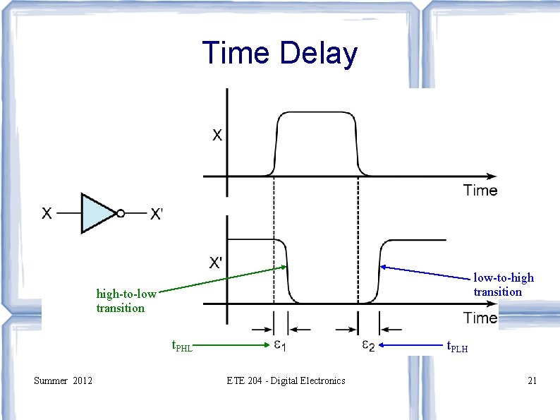
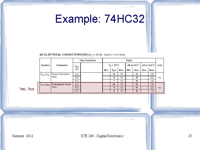
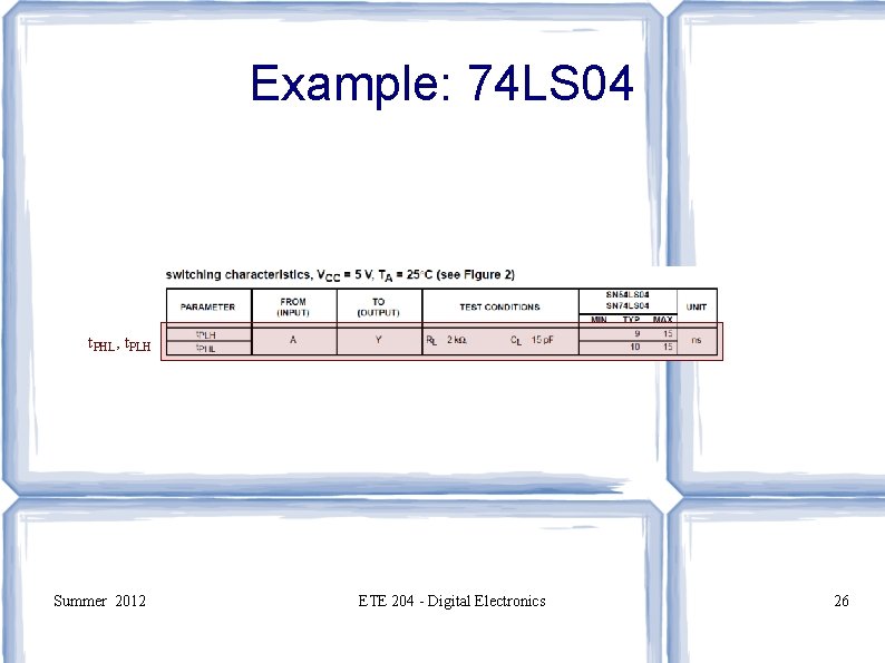
Time Delay (aka. Latency) A standard logic gate does not respond to a change on one of its inputs instantaneously. There is, instead, a finite delay between a change on the input and a change on the output. The propagation delay of a standard logic gate is defined for two cases: t. PLH = delay for output to change from low to high t. PHL = delay for output to change from high to low Summer 2012 ETE 204 - Digital Electronics 20

Time Delay low-to-high transition high-to-low transition t. PHL Summer 2012 t. PLH ETE 204 - Digital Electronics 21

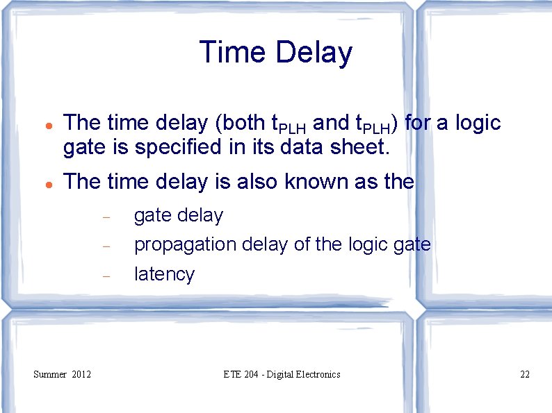
Time Delay The time delay (both t. PLH and t. PLH) for a logic gate is specified in its data sheet. The time delay is also known as the Summer 2012 gate delay propagation delay of the logic gate latency ETE 204 - Digital Electronics 22

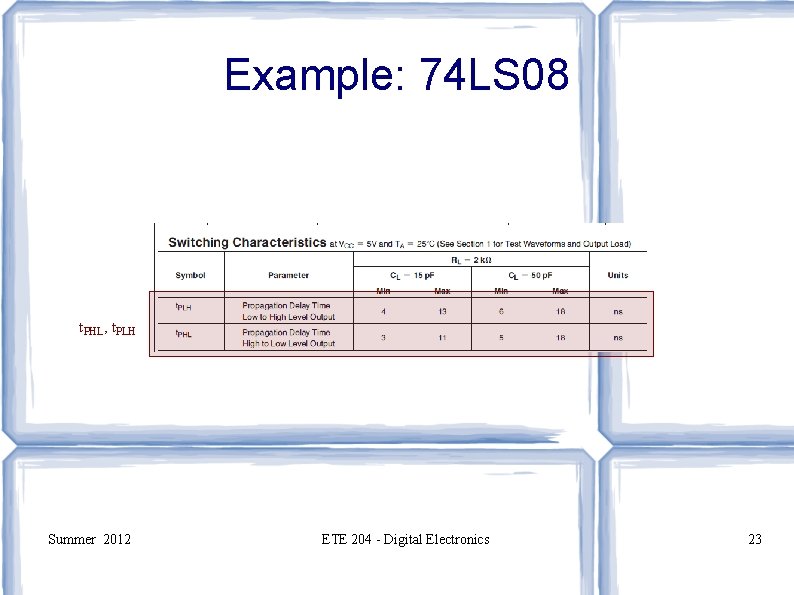
Example: 74 LS 08 t. PHL, t. PLH Summer 2012 ETE 204 - Digital Electronics 23

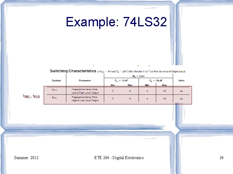
Example: 74 LS 32 t. PHL, t. PLH Summer 2012 ETE 204 - Digital Electronics 24

Example: 74 HC 32 t. PHL, t. PLH Summer 2012 ETE 204 - Digital Electronics 25

Example: 74 LS 04 t. PHL, t. PLH Summer 2012 ETE 204 - Digital Electronics 26

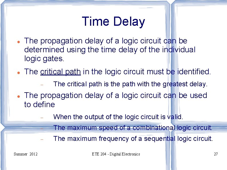
Time Delay The propagation delay of a logic circuit can be determined using the time delay of the individual logic gates. The critical path in the logic circuit must be identified. The critical path is the path with the greatest delay. The propagation delay of a logic circuit can be used to define Summer 2012 When the output of the logic circuit is valid. The maximum speed of a combinational logic circuit. The maximum frequency of a sequential logic circuit. ETE 204 - Digital Electronics 27

Questions? Summer 2012 ETE 204 - Digital Electronics 28