EtchStop Techniques 1 Doping Selective Etching DSE A
 Doping Selective Etching (DSE) • A region at which wet")


 Conventional Bias-Dependent DSE or Electrochemical Etch-Stop Definition : In electrochemical")
 injection of holes into Si")
 PP")


 Photovoltaic Electrochemical Etchstop Technique (PHET) • PHET is able to")
 : An Array of Thin Membranes (I) Objectve : To use electrochemical")
 Process :")
 Cantilever Beam Fabrication : (a) The Diffused Pattern Technique Process Flow :")
 Cantilever Beam Fabrication : (b) The Etched Pattern Technique Process Flow :")

 : Half Circle Structures Diffused Pattern Technique Etched Pattern Technique")
- Slides: 17
Etch-Stop Techniques : (1) Doping Selective Etching (DSE) • A region at which wet etching tends to slow down or diminish is called an "etch-stop". • An example of an etch-stop region is a thin heavily B-doped layer, which is epitaxially-grown or is formed by diffusion or implantation, on a lightly-doped substrate : this method of creating an etch-stop is called doping-selective etching (DSE). • This stopping effect is a general property of basic etching solutions such as KOH, Na. OH, ethylenediamine pyrocatechol (EDP), and hydrazine. • Due to heavily B-doping the lattice constant of Si decreases slightly. This leads to highly strained membranes often showing slip planes. They are, however, taut and fairly rugged even in a few microns thickness and ~ 1 cm diameter.
Dopant-Dependent Etch Rates for Silicon
B-Doping Etch-Stop for Common Etchants
• DSE is typically exploited for undercutting microstructures defined by a masked heavy boron diffusion in an n-type or p-type substrate. • If the etch-stop concentration threshold lies in between the substrate and diffusion concentrations, the p- (or n-) substrate is etched out from underneath the high boron diffusion layer ; hence, a Si microstructure with a geometry defined by the diffusion mask and a thickness close to the diffusion depth is left freely suspended. • Advantages of DSE : (i) independence of crystal orientation, (ii) smooth surface finish, (iii) offers the possibilities for fabricating release structures with arbitrary lateral geometry in a single etch step. • Disadvantages of DSE : (i) high B doses required introduce mechanical stress into the material, (ii) introduction of electrical components for sensing purposes into these microstructures, such as implantation of piezoresistors, is inhibited by the excessive background doping.
Etch-Stop Techniques : (2) Conventional Bias-Dependent DSE or Electrochemical Etch-Stop Definition : In electrochemical etching method a voltage is applied over the Si wafer and a counter-electrode in etching solution. Linden etal. , Sensors and Actuators 16, 67 (1989)
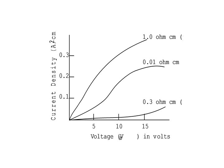
• The fundamental steps of etching : (i) injection of holes into Si to raise it to a higher oxidation state Si+, (ii) attachment of hydroxyl groups (OH)- to positively-charged Si, (iii) reaction of hydrated Si with the complexing agent in the solution, and (4) dissolution of the reacted products into the etching solution. • In bias-dependent etching oxidation is promoted by a voltage applied to the Si wafer, which causes an accumulation of holes in the Si/solution interface. • Holes transported to the negative electrode as H+ ions, and are released there as hydrogen gas bubbles. • Excess electron-hole pairs can, in addition, be created at the Si surface, e. g. , by optical excitation, thereby increasing the etch rate.
The Mechanisms of Bias-Dependent Etching OCP = open circuit potential (I = 0) PP = passivating potential.
• The conventional electrochemical etch-stop technique is attractive for fabricating microstructures since it has the potential for allowing one to reproducibly fabricate moderately doped n-type Si structures with good thickness control. BUT • Since the difference of PP between n- and p-type Si is only a few tenths of a volt, the control of the etch-stop is critical. • Since the selectivity between n-type and p-type Si in this process is achieved through the current blocking action of the pn diode, any leakage in this diode will affect the selectivity. • If the leakage current is very large, it is possible for etching to terminate well before the junction is reached.
Possible Solution : Four-electrode Configuration • The p-Si is 1. 1 V negative with respect to the reference (RE) which is at the potential of the solution : p-Si will be etched. • The n-Si is 0. 3 V positive with respect to RE. This value is far enough positive from PP point : as soon as n-Si is exposed to solution it will be passivated. • Any leakage current through the diode will be drained of by Vrb and will not leak into the solution.
Etch-Stop Techniques : (4) Photovoltaic Electrochemical Etchstop Technique (PHET) • PHET is able to produce the majority of structures that can be produced by either the high boron or the electrochemical etchstop. • PHET does not require the high impurity concentrations of the boron etchstop, and external electrodes as in conventional or pulsed anodization electrochemical etchstop techniques. • Essentially PHET is a two-electrode electrochemical etchstop in which the potential and current required for anodic growth of a passivating oxide is not applied externally, but is generated within the silicon itself. • The passivation potential consists of two components ; (1) the photovoltage across an illuminated pn junction and the "Nernest" potential of an n-Si/metal/etchant solution electrochemical cell. Peeters etal. , JMEMS 3, 113 (1994)
Example (4) : An Array of Thin Membranes (I) Objectve : To use electrochemical etching to fabricate an array of membranes with thicknesses in the range 3 to 8 mm and sides that are between 0. 5 and 5 mm. The array is to be fabricated on a p-type Si substrate. Linden etal. , Sensors and Actuators 16, 67 (1989)
(II) Process :
Example (5) Cantilever Beam Fabrication : (a) The Diffused Pattern Technique Process Flow : Linden etal. , Sensors and actuators (16), 67 (1989)
Example (6) Cantilever Beam Fabrication : (b) The Etched Pattern Technique Process Flow :
The Deflection of the Beam with a Diamond Stylus Providing the Applied Force • The beam has a length of 2 mm and a thickness of 15 mm. • The distance from the surface of the wafer to the bottom of the cavity is 300 mm.
Example (7) : Half Circle Structures Diffused Pattern Technique Etched Pattern Technique