Etching Chapters 11 20 21 we will return
- Slides: 38

Etching Chapters 11, 20, 21 (we will return to this topic in MEMS) sami. franssila@aalto. fi

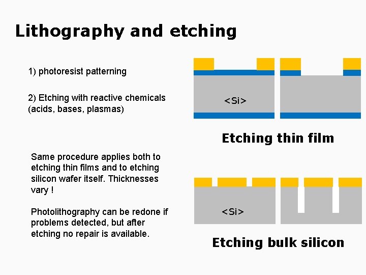
Lithography and etching 1) photoresist patterning 2) Etching with reactive chemicals (acids, bases, plasmas) <Si> Etching thin film Same procedure applies both to etching thin films and to etching silicon wafer itself. Thicknesses vary ! Photolithography can be redone if problems detected, but after etching no repair is available. <Si> Etching bulk silicon

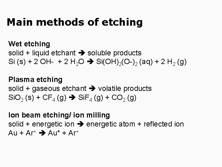
Main methods of etching Wet etching solid + liquid etchant soluble products Si (s) + 2 OH- + 2 H 2 O Si(OH)2(O-)2 (aq) + 2 H 2 (g) Plasma etching solid + gaseous etchant volatile products Si. O 2 (s) + CF 4 (g) Si. F 4 (g) + CO 2 (g) Ion beam etching/ ion milling solid + energetic ion energetic atom + reflected ion Au + Ar+ Au* + Ar+

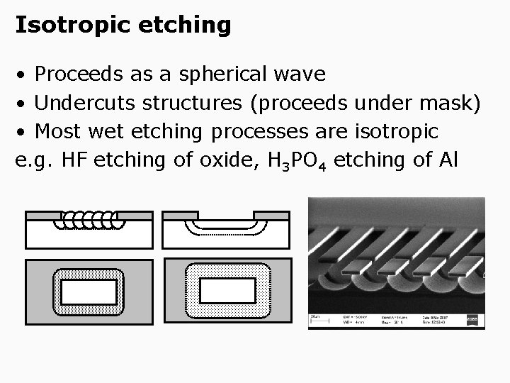
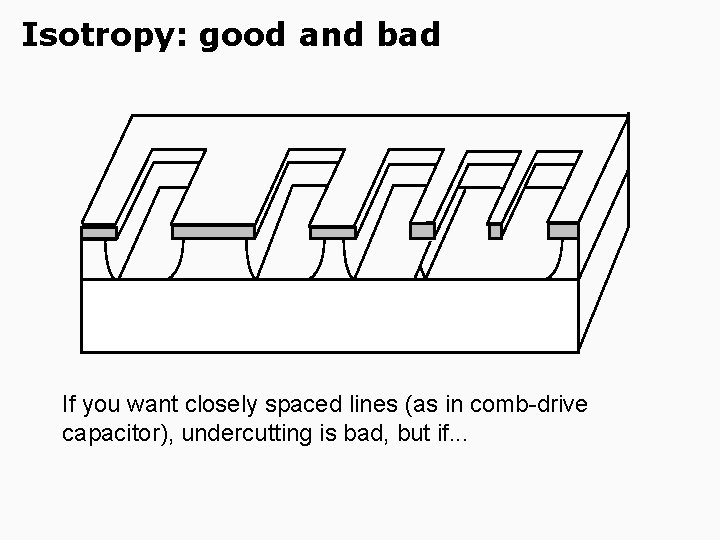
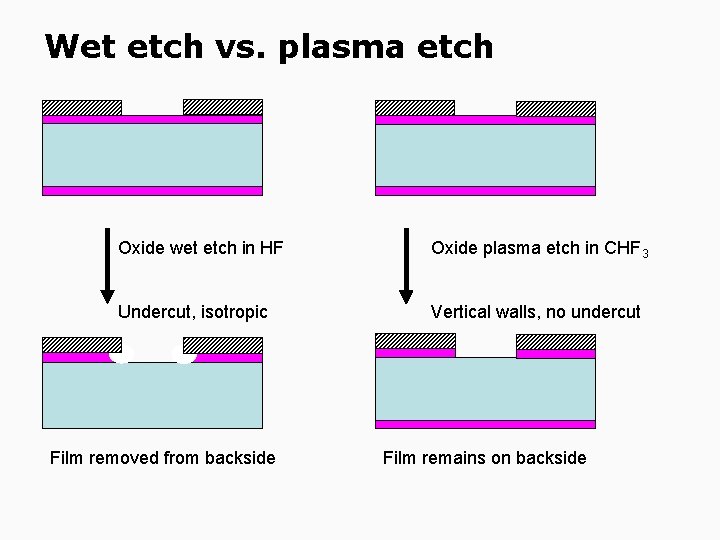
Isotropic etching • Proceeds as a spherical wave • Undercuts structures (proceeds under mask) • Most wet etching processes are isotropic e. g. HF etching of oxide, H 3 PO 4 etching of Al

Isotropy: good and bad If you want closely spaced lines (as in comb-drive capacitor), undercutting is bad, but if. . .

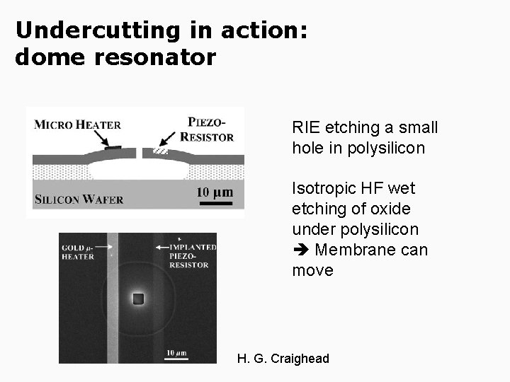
Undercutting in action: dome resonator RIE etching a small hole in polysilicon Isotropic HF wet etching of oxide under polysilicon Membrane can move H. G. Craighead

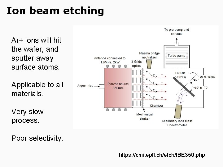
Ion beam etching Ar+ ions will hit the wafer, and sputter away surface atoms. Applicable to all materials. Very slow process. Poor selectivity. https: //cmi. epfl. ch/etch/IBE 350. php

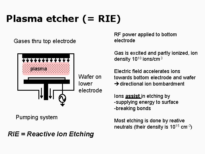
Plasma etcher (= RIE) RF power applied to bottom electrode Gases thru top electrode Gas is excited and partly ionized, ion density 1010 ions/cm 3 plasma Wafer on lower electrode Pumping system RIE = Reactive Ion Etching Electric field accelerates ions towards bottom electrode and wafer directional ion bombardment Ions assist in etching by -supplying energy to surface -breaking bonds Most etching is done by reative neutrals (their density is 1015 cm-3)

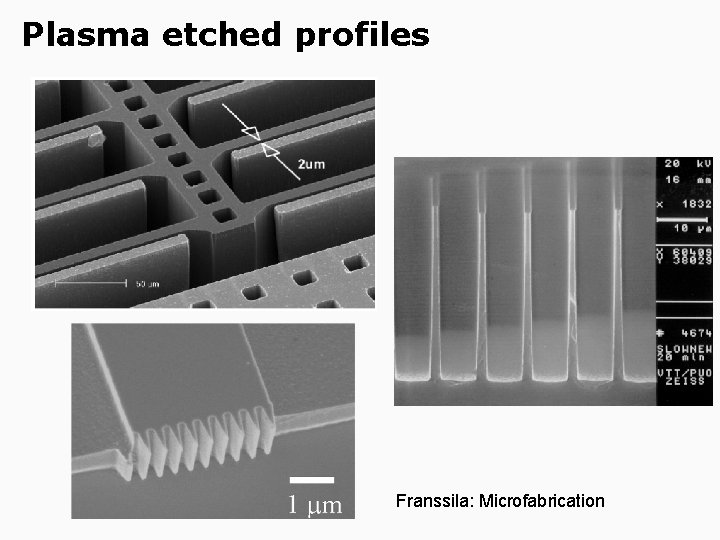
Plasma etched profiles Franssila: Microfabrication

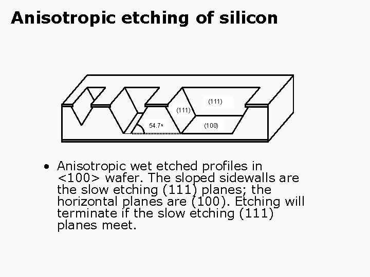
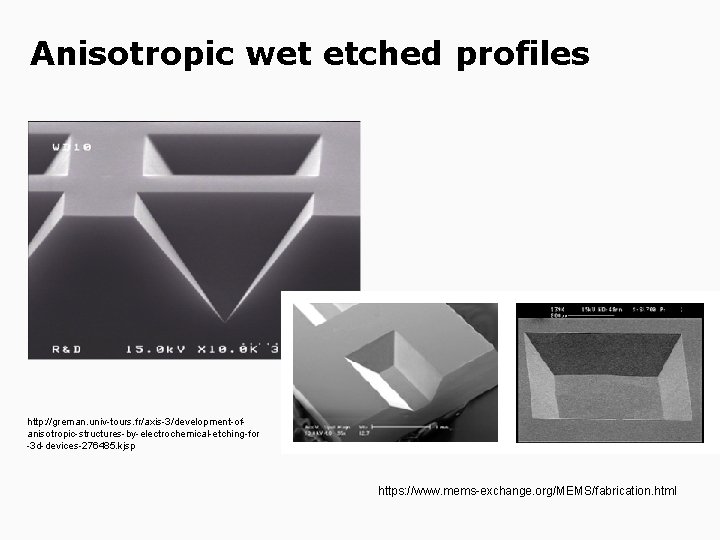
Anisotropic etching of silicon (111) 54. 7 o (100) • Anisotropic wet etched profiles in <100> wafer. The sloped sidewalls are the slow etching (111) planes; the horizontal planes are (100). Etching will terminate if the slow etching (111) planes meet.

Anisotropic wet etched profiles http: //greman. univ-tours. fr/axis-3/development-ofanisotropic-structures-by-electrochemical-etching-for -3 d-devices-276485. kjsp https: //www. mems-exchange. org/MEMS/fabrication. html

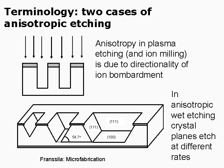
Terminology: two cases of anisotropic etching Anisotropy in plasma etching (and ion milling) is due to directionality of ion bombardment (111) 54. 7 o Franssila: Microfabrication (100) In anisotropic wet etching crystal planes etch at different rates

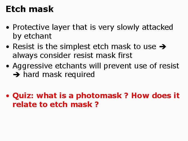
Etch mask • Protective layer that is very slowly attacked by etchant • Resist is the simplest etch mask to use always consider resist mask first • Aggressive etchants will prevent use of resist hard mask required • Quiz: what is a photomask ? How does it relate to etch mask ?

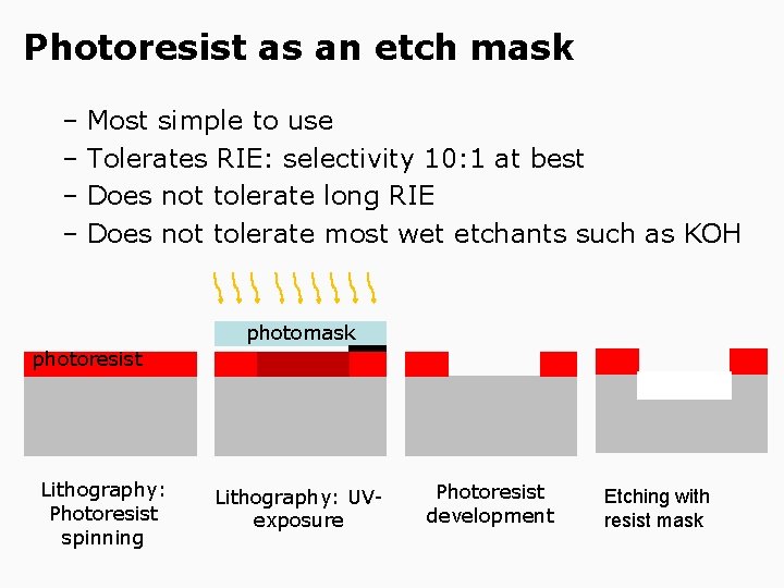
Photoresist as an etch mask – Most simple to use – Tolerates RIE: selectivity 10: 1 at best – Does not tolerate long RIE – Does not tolerate most wet etchants such as KOH photomask photoresist Lithography: Photoresist spinning Lithography: UVexposure Photoresist development Etching with resist mask

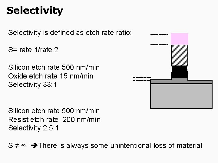
Selectivity is defined as etch rate ratio: S= rate 1/rate 2 Silicon etch rate 500 nm/min Oxide etch rate 15 nm/min Selectivity 33: 1 Silicon etch rate 500 nm/min Resist etch rate 200 nm/min Selectivity 2. 5: 1 S ≠ ∞ There is always some unintentional loss of material

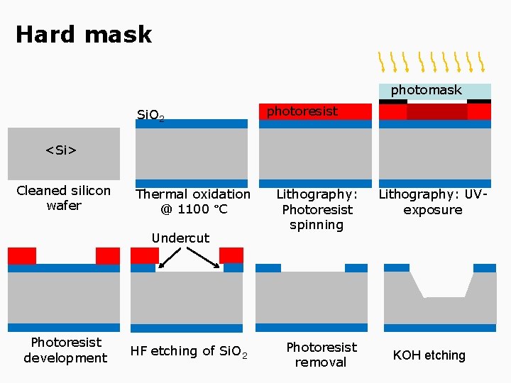
Hard mask photomask Si. O 2 photoresist <Si> Cleaned silicon wafer Thermal oxidation @ 1100 °C Undercut Photoresist development HF etching of Si. O 2 Lithography: Photoresist spinning Photoresist removal Lithography: UVexposure KOH etching

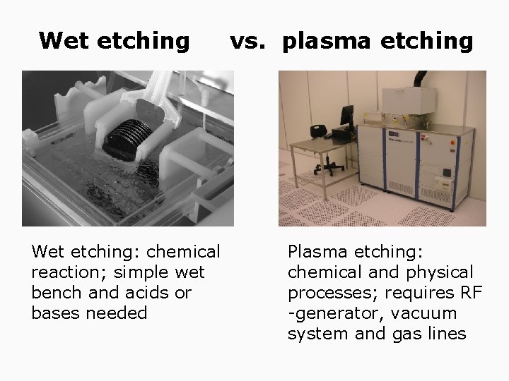
Wet etching: chemical reaction; simple wet bench and acids or bases needed vs. plasma etching Plasma etching: chemical and physical processes; requires RF -generator, vacuum system and gas lines

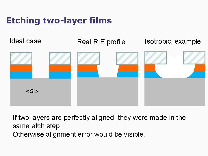
Etching two-layer films Ideal case Real RIE profile Isotropic, example <Si> If two layers are perfectly aligned, they were made in the same etch step. Otherwise alignment error would be visible.

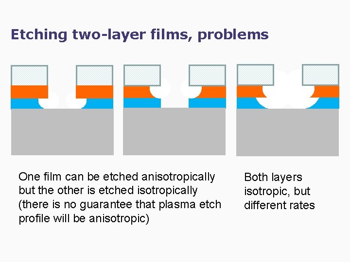
Etching two-layer films, problems <Si> One film can be etched anisotropically but the other is etched isotropically (there is no guarantee that plasma etch profile will be anisotropic) Both layers isotropic, but different rates

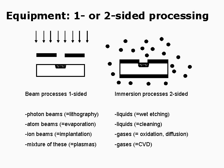
Equipment: 1 - or 2 -sided processing Beam processes 1 -sided Immersion processes 2 -sided -photon beams (=lithography) -liquids (=wet etching) -atom beams (=evaporation) -liquids (=cleaning) -ion beams (=implantation) -gases (= oxidation, diffusion) -mixture of these (=plasmas) -gases (=CVD)

Wet etch vs. plasma etch Oxide wet etch in HF Oxide plasma etch in CHF 3 Undercut, isotropic Vertical walls, no undercut Film removed from backside Film remains on backside

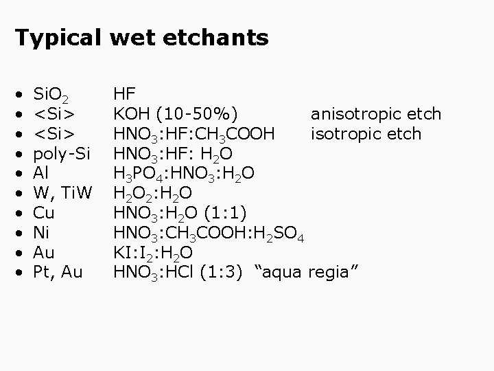
Typical wet etchants • • • Si. O 2 <Si> poly-Si Al W, Ti. W Cu Ni Au Pt, Au HF KOH (10 -50%) anisotropic etch HNO 3: HF: CH 3 COOH isotropic etch HNO 3: HF: H 2 O H 3 PO 4: HNO 3: H 2 O 2: H 2 O HNO 3: H 2 O (1: 1) HNO 3: CH 3 COOH: H 2 SO 4 KI: I 2: H 2 O HNO 3: HCl (1: 3) “aqua regia”

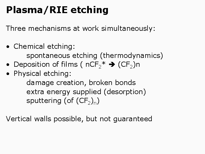
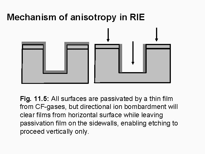
Plasma/RIE etching Three mechanisms at work simultaneously: • Chemical etching: spontaneous etching (thermodynamics) • Deposition of films ( n. CF 2* (CF 2)n • Physical etching: damage creation, broken bonds extra energy supplied (desorption) sputtering (of (CF 2)n) Vertical walls possible, but not guaranteed

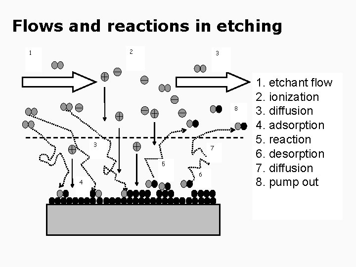
Flows and reactions in etching 2 1 3 8 3 7 5 4 6 1. etchant flow 2. ionization 3. diffusion 4. adsorption 5. reaction 6. desorption 7. diffusion 8. pump out

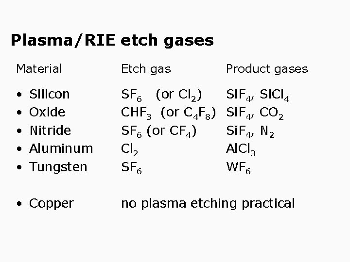
Plasma/RIE etch gases Material Etch gas Product gases • • • SF 6 (or Cl 2) CHF 3 (or C 4 F 8) SF 6 (or CF 4) Cl 2 SF 6 Si. F 4, Si. Cl 4 Si. F 4, CO 2 Si. F 4, N 2 Al. Cl 3 WF 6 Silicon Oxide Nitride Aluminum Tungsten • Copper no plasma etching practical

Mechanism of anisotropy in RIE Fig. 11. 5: All surfaces are passivated by a thin film from CF-gases, but directional ion bombardment will clear films from horizontal surface while leaving passivation film on the sidewalls, enabling etching to proceed vertically only.

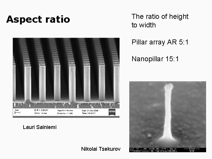
The ratio of height to width Aspect ratio Pillar array AR 5: 1 Nanopillar 15: 1 Lauri Sainiemi Nikolai Tsekurov

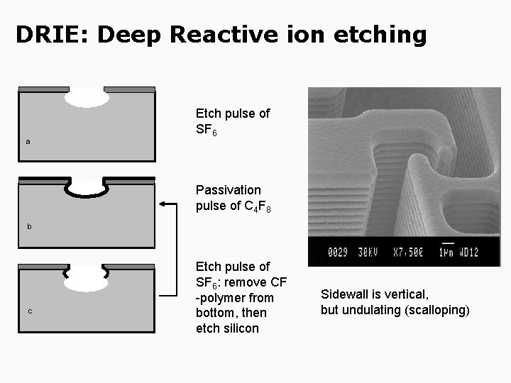
DRIE: Deep Reactive ion etching a Etch pulse of SF 6 Passivation pulse of C 4 F 8 b c Etch pulse of SF 6: remove CF -polymer from bottom, then etch silicon Sidewall is vertical, but undulating (scalloping)

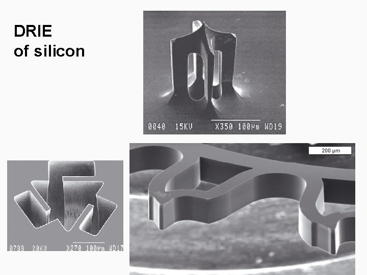
DRIE of silicon

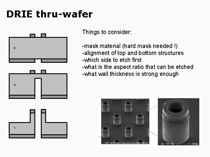
DRIE thru-wafer Things to consider: a b c -mask material (hard mask needed !) -alignment of top and bottom structures -which side to etch first -what is the aspect ratio that can be etched -what wall thickness is strong enough

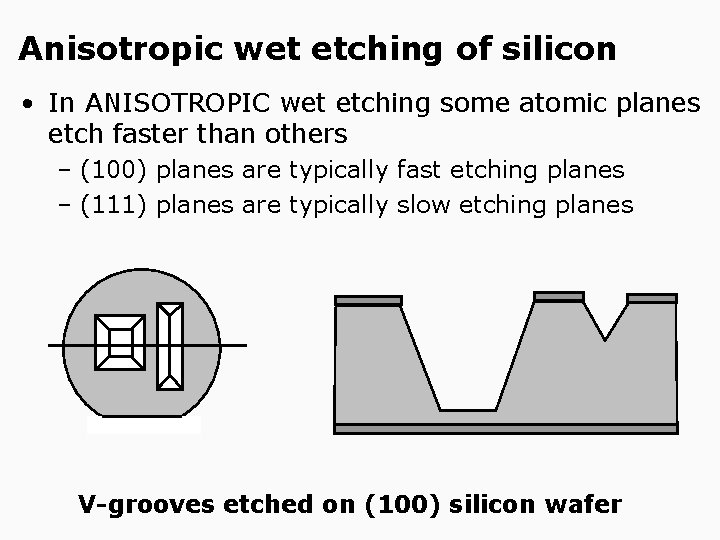
Anisotropic wet etching of silicon • In ANISOTROPIC wet etching some atomic planes etch faster than others – (100) planes are typically fast etching planes – (111) planes are typically slow etching planes V-grooves etched on (100) silicon wafer

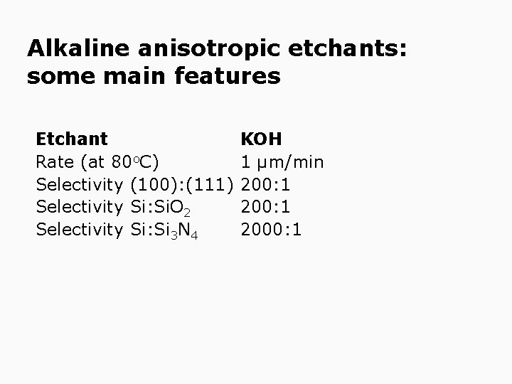
Alkaline anisotropic etchants: some main features Etchant Rate (at 80 o. C) Selectivity (100): (111) Selectivity Si: Si. O 2 Selectivity Si: Si 3 N 4 KOH 1 µm/min 200: 1 2000: 1

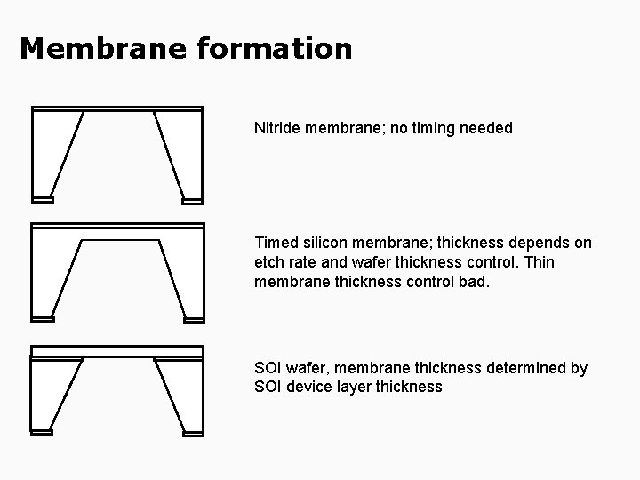
Membrane formation Nitride membrane; no timing needed Timed silicon membrane; thickness depends on etch rate and wafer thickness control. Thin membrane thickness control bad. SOI wafer, membrane thickness determined by SOI device layer thickness

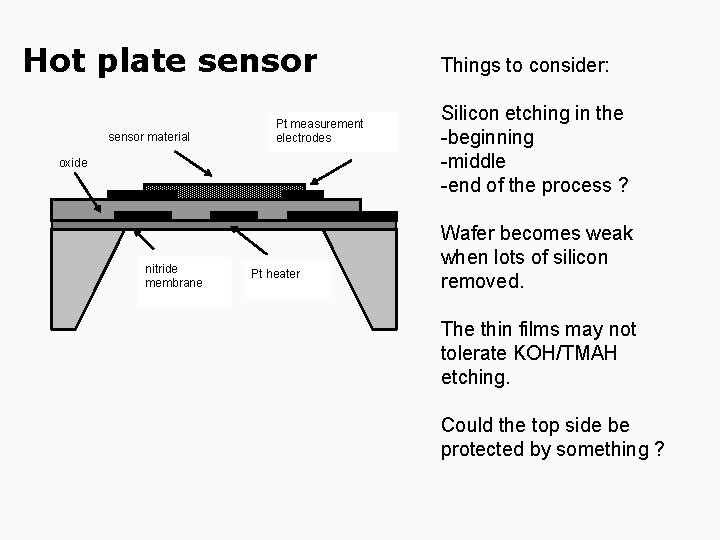
Hot plate sensor material Pt measurement electrodes oxide nitride membrane Pt heater Things to consider: Silicon etching in the -beginning -middle -end of the process ? Wafer becomes weak when lots of silicon removed. The thin films may not tolerate KOH/TMAH etching. Could the top side be protected by something ?

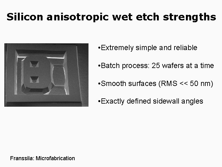
Silicon anisotropic wet etch strengths • Extremely simple and reliable • Batch process: 25 wafers at a time • Smooth surfaces (RMS << 50 nm) • Exactly defined sidewall angles Franssila: Microfabrication

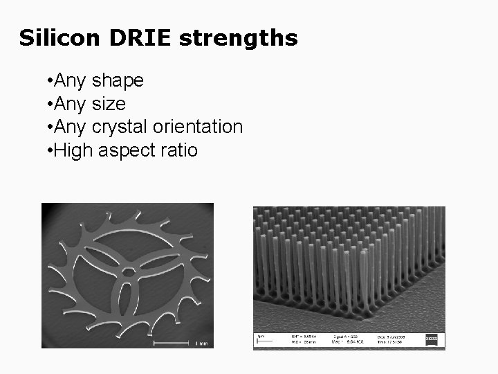
Silicon DRIE strengths • Any shape • Any size • Any crystal orientation • High aspect ratio

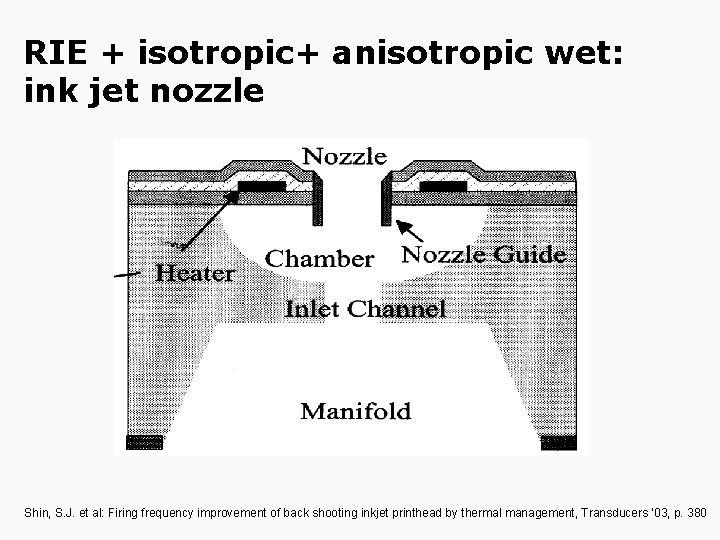
RIE + isotropic+ anisotropic wet: ink jet nozzle Shin, S. J. et al: Firing frequency improvement of back shooting inkjet printhead by thermal management, Transducers ’ 03, p. 380

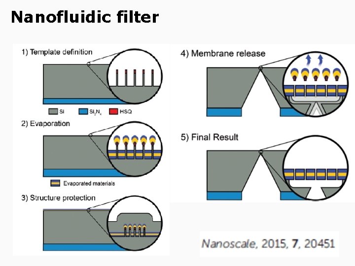
Nanofluidic filter