ESSCIRCESSDERC 2019 Presentation A Template Name and Surname
- Slides: 12

ESSCIRC/ESSDERC 2019 Presentation (A Template) Name and Surname Department Name Institution Name, Country email@institute. com September 23 -26, 2019 ESSCIRC/ESSDERC 2019, Cracow, Poland 1 of 12

Outline o Text and Figures Template n n n Font sizes, bullets, sub-bullets drawing line thicknesses, waveforms and graphs Use of figures, colors Name Surname ESSCIRC/ESSDERC 2019, Cracow, Poland 2 of 12

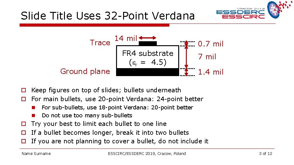
Slide Title Uses 32 -Point Verdana Trace Ground plane 14 mil FR 4 substrate (er = 4. 5) 0. 7 mil 1. 4 mil o Keep figures on top of slides; bullets underneath o For main bullets, use 20 -point Verdana: 24 -point better n n For sub-bullets, use 18 -point Verdana: 20 -point better Do not use too many sub-bullets o Try your best to limit each bullet to one line o If a bullet becomes longer, break it into two bullets o If you are not planning to cover a bullet, do not include it Name Surname ESSCIRC/ESSDERC 2019, Cracow, Poland 3 of 12

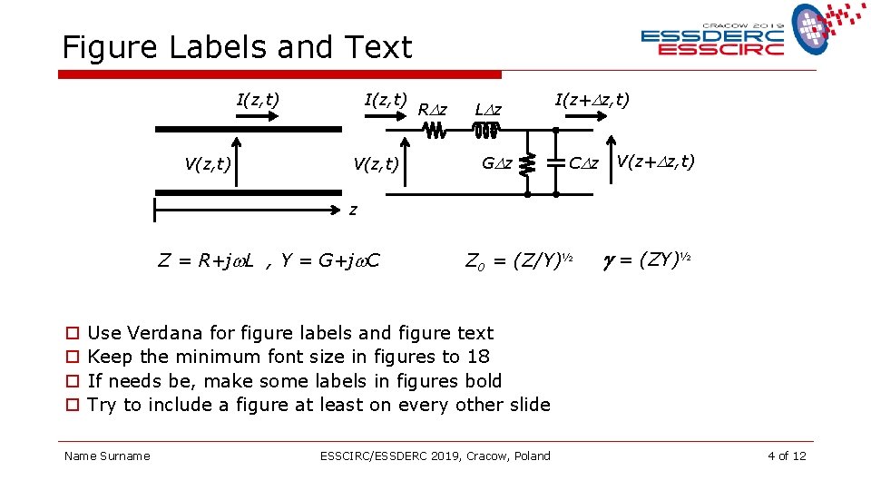
Figure Labels and Text I(z, t) V(z, t) RD z LDz GD z I(z+Dz, t) CD z V(z+Dz, t) z Z = R+jw. L , Y = G+jw. C o o Z 0 = (Z/Y)½ g = (ZY)½ Use Verdana for figure labels and figure text Keep the minimum font size in figures to 18 If needs be, make some labels in figures bold Try to include a figure at least on every other slide Name Surname ESSCIRC/ESSDERC 2019, Cracow, Poland 4 of 12

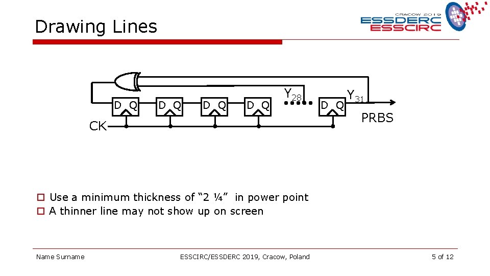
Drawing Lines D Q D Q Y 28 CK D Q Y 31 PRBS o Use a minimum thickness of “ 2 ¼” in power point o A thinner line may not show up on screen Name Surname ESSCIRC/ESSDERC 2019, Cracow, Poland 5 of 12

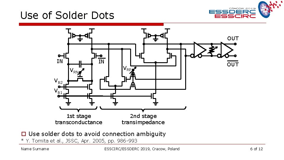
Use of Solder Dots OUT IN IN VRP OUT VB 2 VB 1 1 st stage transconductance 2 nd stage transimpedance o Use solder dots to avoid connection ambiguity * Y. Tomita et al. , JSSC, Apr. 2005, pp. 986 -993 Name Surname ESSCIRC/ESSDERC 2019, Cracow, Poland 6 of 12

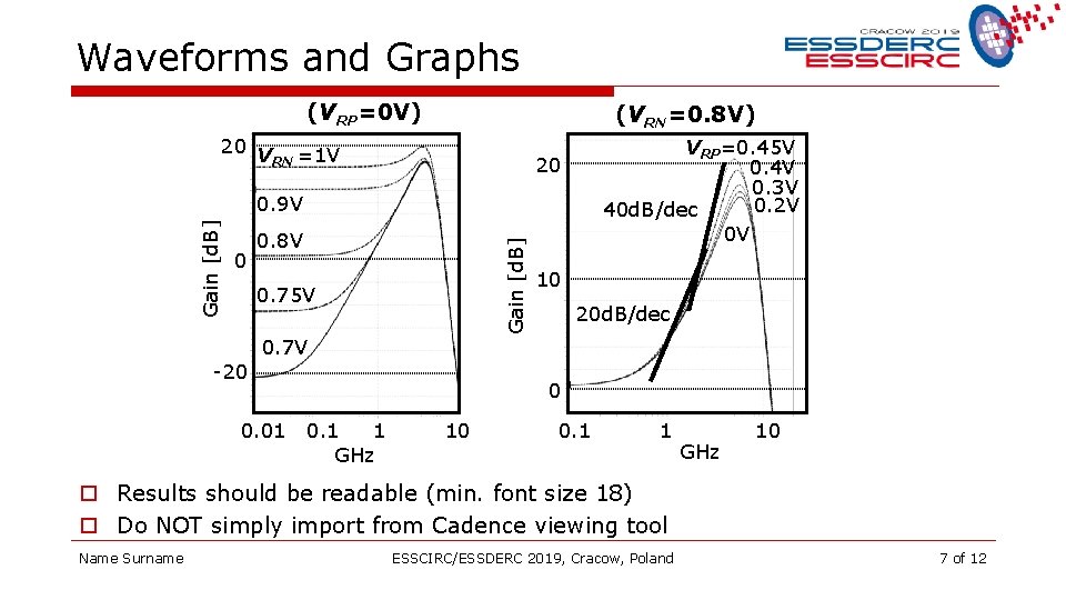
Waveforms and Graphs (VRP=0 V) (VRN=0. 8 V) 20 V =1 V RN VRP=0. 45 V 0. 4 V 0. 3 V 0. 2 V 40 d. B/dec 0 V 20 0 0. 8 V Gain [d. B] 0. 9 V 0. 75 V -20 10 20 d. B/dec 0. 7 V 0. 01 0 0. 1 1 GHz 10 o Results should be readable (min. font size 18) o Do NOT simply import from Cadence viewing tool Name Surname ESSCIRC/ESSDERC 2019, Cracow, Poland 7 of 12

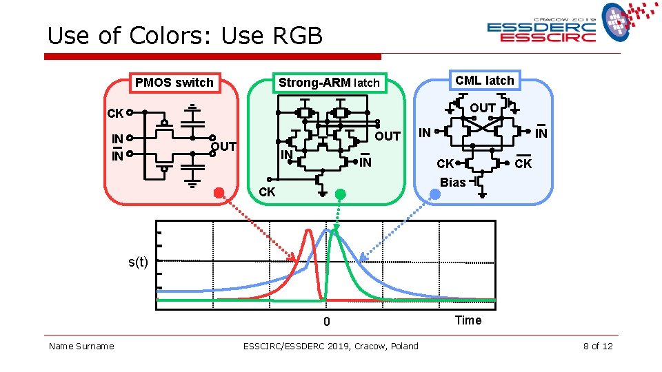
Use of Colors: Use RGB PMOS switch CML latch Strong-ARM latch OUT CK IN IN OUT IN IN CK Bias CK s(t) 0 Name Surname ESSCIRC/ESSDERC 2019, Cracow, Poland Time 8 of 12

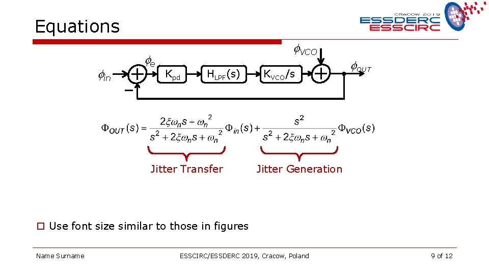
Equations fin fe f. VCO Kpd HLPF(s) Jitter Transfer KVCO/s f. OUT Jitter Generation o Use font size similar to those in figures Name Surname ESSCIRC/ESSDERC 2019, Cracow, Poland 9 of 12

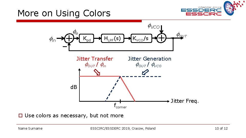
More on Using Colors fin fe f. VCO Kpd HLPF(s) Jitter Transfer f. OUT / fin f. OUT KVCO/s Jitter Generation f. OUT / f. VCO d. B fcorner Jitter Freq. o Use colors as necessary, but not more Name Surname ESSCIRC/ESSDERC 2019, Cracow, Poland 10 of 12

Papers to See This Year Suggest papers based on Advance Program o 11. 3, 11. 4: good example on burst-mode CDR Session 5 Relevant Papers: o 5. 1: 8 Gb/s 5 -FFE, analog EQ, 2 -DFE, eye-tracking CDR o 5. 2: 40 Gb/s adaptive EQ and CDR Session 25 Relevant Paper: o 25. 9: 8 x 3. 2 Gb/s link with collaborative timing recovery Name Surname ESSCIRC/ESSDERC 2019, Cracow, Poland 11 of 12

Include Key References o o o o o Razavi, “Design of Integrated Circuits for Optical Communications, ” Mc. Graw Hill, 2003. R. C. Walker, “Designing Bang-Bang PLL’s for Clock and Data Recovery in Serial Data Transmission Systems, ” B. Razavi, Ed: IEEE Press, 2003, pp. 34 -45. L. De. Vito et al. , “A 52 MHz and 155 MHz clock-recovery PLL, ”, ISSCC 1991, paper 8. 6 Y. M. Greshishchev et al. , “A Fully Integrated Si. Ge Receiver IC for 10 Gb/s Data Rate”, ISSCC 2000, paper 3. 2. Expanded version in JSSC, Dec. 2000, pp. 1949 -1957. J. Lee et al. , “Analysis and Modeling of Bang-Bang Clock and Data Recovery Circuits, ” JSSC, Sep. 2004, pp. 1571 -2004. H. Takauchi et al. , “A CMOS Multichannel 10 -Gb/s Transceiver, ” ISSCC 2003, paper 4. 2. Expanded version in JSSC, Dec. 2003, pp. 2094 -2100. N. Nedovic et al. , “A 40 -to-44 Gb/s 3 x Oversampling CDR 1: 16/DEMUX, ” ISSCC 2007, paper 12. 2. Expanded version in JSSC, Dec. 2007, pp. 2726 -2735. M. van Ierssel et al. , “A 3. 2 Gb/s Semi-Blind-Oversampling CDR”, ISSCC 2006, paper 18. 5. Expanded version in JSSC, Oct. 2007, pp. 2224 -2234. T. H. Lee et al. , “A 155 -MHz Clock Recover- and Phase-Locked Loop, ” JSSC, Dec. 1992, pp. 17361746. J. Mc. Neill, “Jitter in Ring Oscillators, ” JSSC, June 1997, pp. 870 -879. Name Surname ESSCIRC/ESSDERC 2019, Cracow, Poland 12 of 12