
ESE 534 Computer Organization Day 7 February 6
ESE 534: Computer Organization Day 7: February 6, 2012 Memories Penn ESE 534 Spring 2012 -- De. Hon 1
Previously… • Arithmetic: addition, subtraction • Reuse: – pipelining – bit-serial (vectorization) • Area/Time Tradeoffs • Latency and Throughput Penn ESE 534 Spring 2012 -- De. Hon 2
Today • Memory – features – Area and delay intuition and modeling – design – technology Penn ESE 534 Spring 2012 -- De. Hon 3
Preclass 1 When is: Penn ESE 534 Spring 2012 -- De. Hon 4
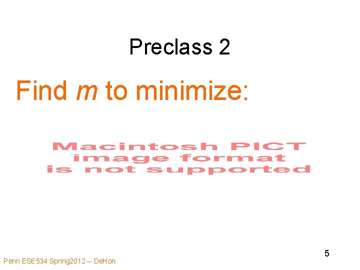
Preclass 2 Find m to minimize: Penn ESE 534 Spring 2012 -- De. Hon 5
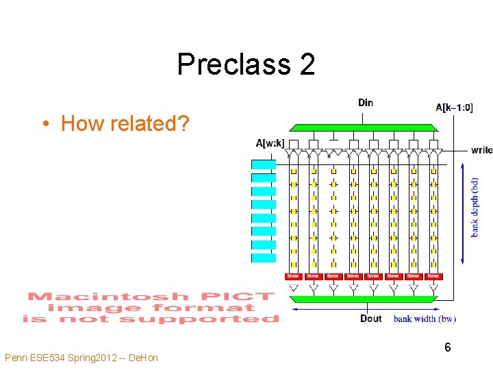
Preclass 2 • How related? Penn ESE 534 Spring 2012 -- De. Hon 6
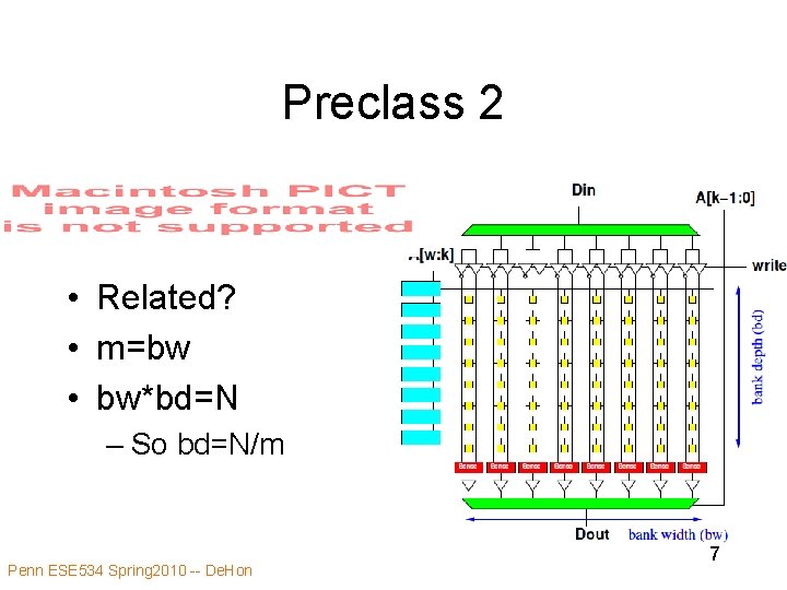
Preclass 2 • Related? • m=bw • bw*bd=N – So bd=N/m Penn ESE 534 Spring 2010 -- De. Hon 7
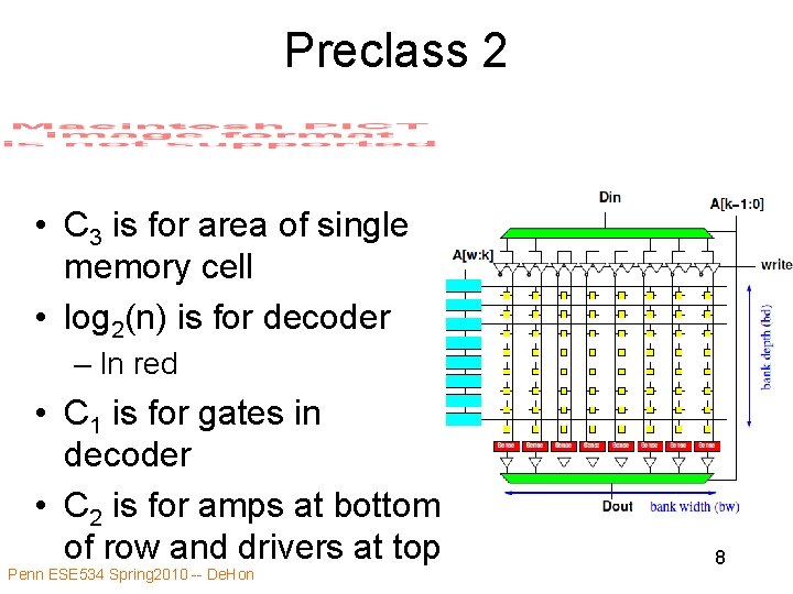
Preclass 2 • C 3 is for area of single memory cell • log 2(n) is for decoder – In red • C 1 is for gates in decoder • C 2 is for amps at bottom of row and drivers at top Penn ESE 534 Spring 2010 -- De. Hon 8
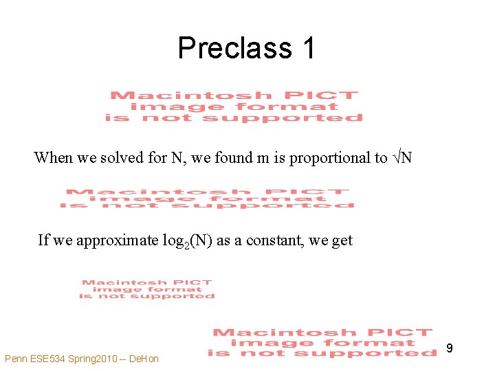
Preclass 1 When we solved for N, we found m is proportional to √N If we approximate log 2(N) as a constant, we get Penn ESE 534 Spring 2010 -- De. Hon 9
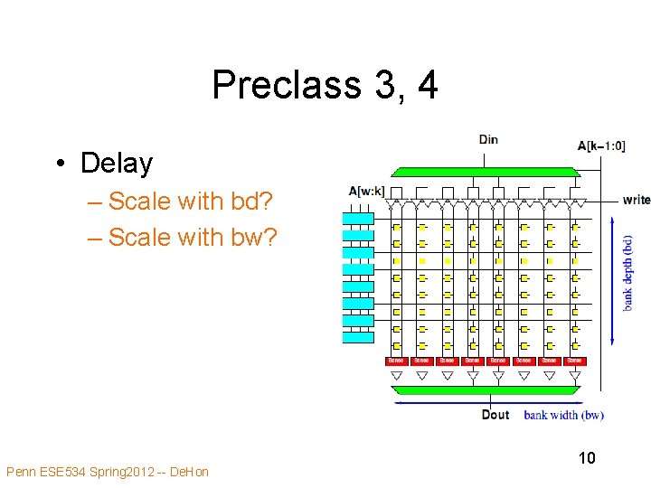
Preclass 3, 4 • Delay – Scale with bd? – Scale with bw? Penn ESE 534 Spring 2012 -- De. Hon 10
Memory • What’s a memory? • What’s special about a memory? Penn ESE 534 Spring 2012 -- De. Hon 11
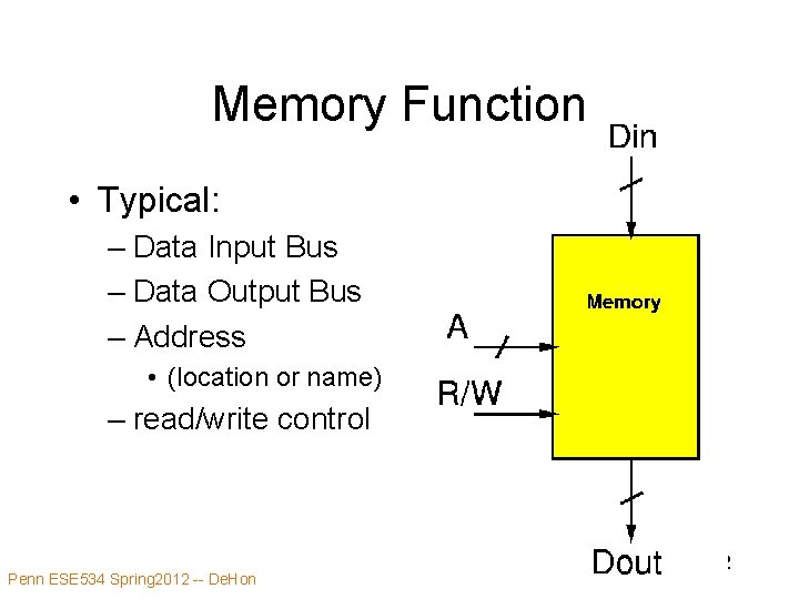
Memory Function • Typical: – Data Input Bus – Data Output Bus – Address • (location or name) – read/write control Penn ESE 534 Spring 2012 -- De. Hon 12
Memory • Block for storing data for later retrieval • State element Penn ESE 534 Spring 2012 -- De. Hon 13
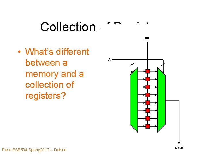
Collection of Registers • What’s different between a memory and a collection of registers? Penn ESE 534 Spring 2012 -- De. Hon 14
Memory Uniqueness • • • Cost Compact state element Packs data very tightly At the expense of sequentializing access Example of Area-Time tradeoff – and a key enabler Penn ESE 534 Spring 2012 -- De. Hon 15
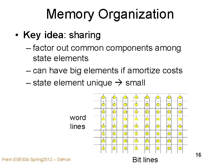
Memory Organization • Key idea: sharing – factor out common components among state elements – can have big elements if amortize costs – state element unique small word lines Penn ESE 534 Spring 2012 -- De. Hon Bit lines 16
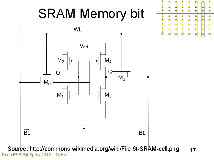
SRAM Memory bit Source: http: //commons. wikimedia. org/wiki/File: 6 t-SRAM-cell. png Penn ESE 534 Spring 2012 -- De. Hon 17
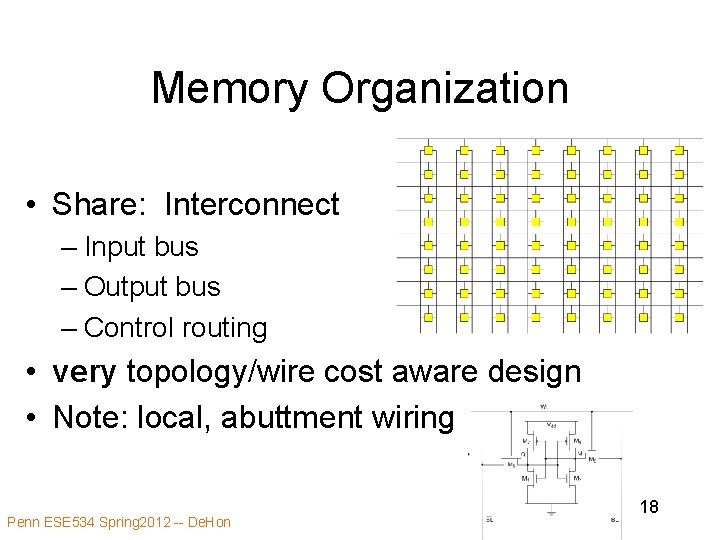
Memory Organization • Share: Interconnect – Input bus – Output bus – Control routing • very topology/wire cost aware design • Note: local, abuttment wiring Penn ESE 534 Spring 2012 -- De. Hon 18
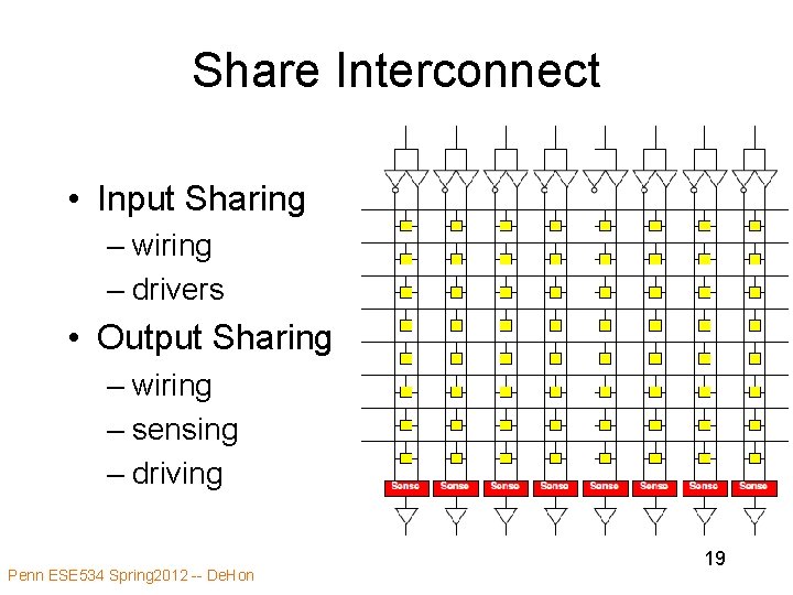
Share Interconnect • Input Sharing – wiring – drivers • Output Sharing – wiring – sensing – driving Penn ESE 534 Spring 2012 -- De. Hon 19
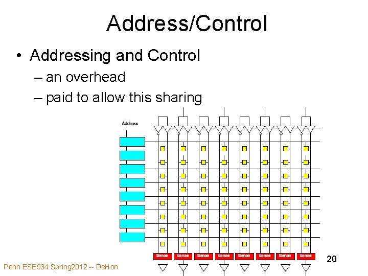
Address/Control • Addressing and Control – an overhead – paid to allow this sharing Penn ESE 534 Spring 2012 -- De. Hon 20
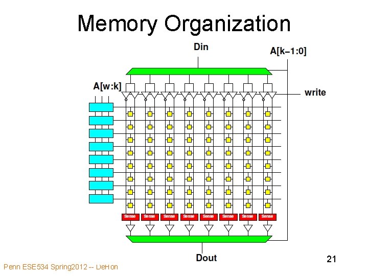
Memory Organization Penn ESE 534 Spring 2012 -- De. Hon 21
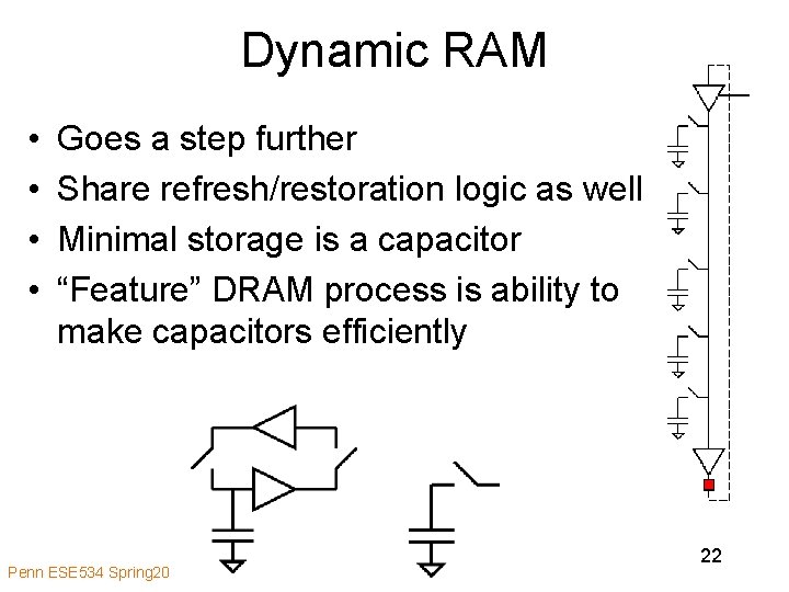
Dynamic RAM • • Goes a step further Share refresh/restoration logic as well Minimal storage is a capacitor “Feature” DRAM process is ability to make capacitors efficiently Penn ESE 534 Spring 2012 -- De. Hon 22
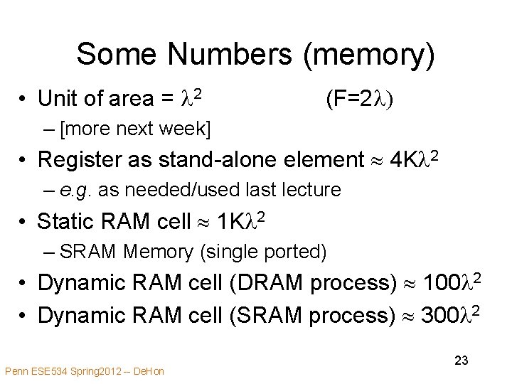
Some Numbers (memory) • Unit of area = l 2 (F=2 l) – [more next week] • Register as stand-alone element 4 Kl 2 – e. g. as needed/used last lecture • Static RAM cell 1 Kl 2 – SRAM Memory (single ported) • Dynamic RAM cell (DRAM process) 100 l 2 • Dynamic RAM cell (SRAM process) 300 l 2 Penn ESE 534 Spring 2012 -- De. Hon 23
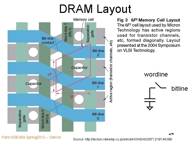
DRAM Layout wordline bitline Penn ESE 534 Spring 2012 -- De. Hon 24 Source: http: //techon. nikkeibp. co. jp/article/HONSHI/20071219/144399/
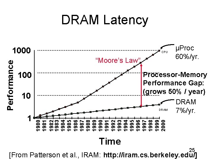
DRAM Latency CPU “Moore’s Law” 100 Processor-Memory Performance Gap: (grows 50% / year) DRAM 7%/yr. 10 1 µProc 60%/yr. 1980 1981 1982 1983 1984 1985 1986 1987 1988 1989 1990 1991 1992 1993 1994 1995 1996 1997 1998 1999 2000 Performance 1000 Time 25 [From Patterson et al. , IRAM: http: //iram. cs. berkeley. edu/] Penn ESE 534 Spring 2012 -- De. Hon
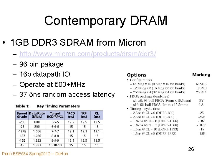
Contemporary DRAM • 1 GB DDR 3 SDRAM from Micron – – – http: //www. micron. com/products/dram/ddr 3/ 96 pin pakage 16 b datapath IO Operate at 500+MHz 37. 5 ns random access latency Penn ESE 534 Spring 2012 -- De. Hon 26
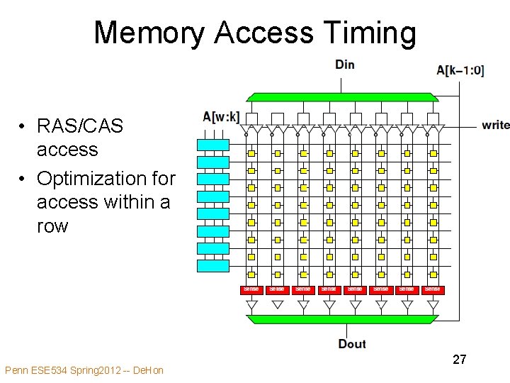
Memory Access Timing • RAS/CAS access • Optimization for access within a row Penn ESE 534 Spring 2012 -- De. Hon 27
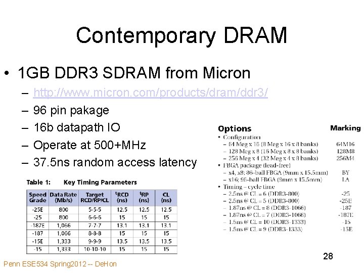
Contemporary DRAM • 1 GB DDR 3 SDRAM from Micron – – – http: //www. micron. com/products/dram/ddr 3/ 96 pin pakage 16 b datapath IO Operate at 500+MHz 37. 5 ns random access latency Penn ESE 534 Spring 2012 -- De. Hon 28
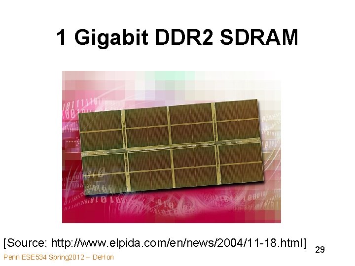
1 Gigabit DDR 2 SDRAM [Source: http: //www. elpida. com/en/news/2004/11 -18. html] Penn ESE 534 Spring 2012 -- De. Hon 29
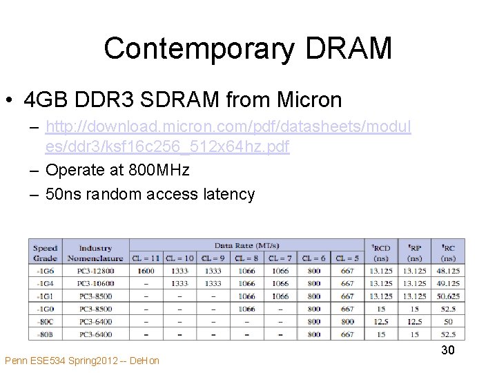
Contemporary DRAM • 4 GB DDR 3 SDRAM from Micron – http: //download. micron. com/pdf/datasheets/modul es/ddr 3/ksf 16 c 256_512 x 64 hz. pdf – Operate at 800 MHz – 50 ns random access latency Penn ESE 534 Spring 2012 -- De. Hon 30
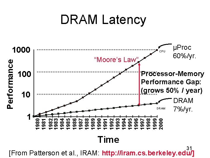
DRAM Latency CPU “Moore’s Law” 100 Processor-Memory Performance Gap: (grows 50% / year) DRAM 7%/yr. 10 1 µProc 60%/yr. 1980 1981 1982 1983 1984 1985 1986 1987 1988 1989 1990 1991 1992 1993 1994 1995 1996 1997 1998 1999 2000 Performance 1000 Time 31 [From Patterson et al. , IRAM: http: //iram. cs. berkeley. edu/] Penn ESE 534 Spring 2012 -- De. Hon
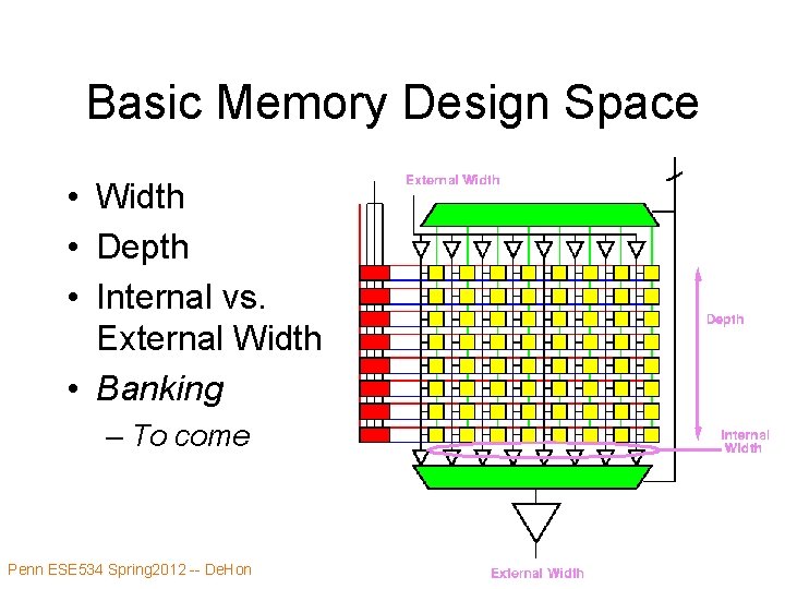
Basic Memory Design Space • Width • Depth • Internal vs. External Width • Banking – To come Penn ESE 534 Spring 2012 -- De. Hon 32
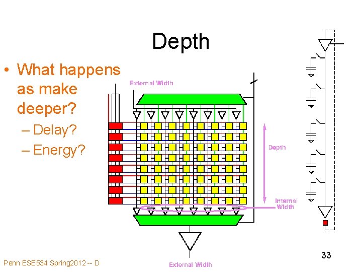
Depth • What happens as make deeper? – Delay? – Energy? Penn ESE 534 Spring 2012 -- De. Hon 33
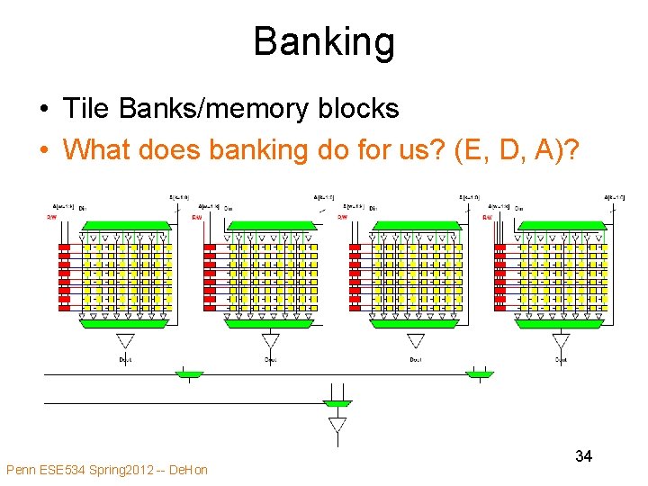
Banking • Tile Banks/memory blocks • What does banking do for us? (E, D, A)? Penn ESE 534 Spring 2012 -- De. Hon 34
Independent Bank Access • Utility? Costs and benefits? Penn ESE 534 Spring 2012 -- De. Hon 35
Memory • Key Idea – Memories hold state compactly – Do so by minimizing key state storage and amortizing rest of structure across large array Penn ESE 534 Spring 2012 -- De. Hon 36
Yesterday vs. Today (Memory Technology) • What’s changed? Penn ESE 534 Spring 2012 -- De. Hon 37
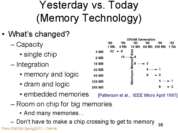
Yesterday vs. Today (Memory Technology) • What’s changed? – Capacity • single chip – Integration • memory and logic • dram and logic • embedded memories [Patterson et al. , – Room on chip for big memories IEEE Micro April 1997] • And many memories… – Don’t have to make a chip crossing to get to memory Penn ESE 534 Spring 2012 -- De. Hon 38
Important Technology Cost • IO between chips << IO on chip – pad spacing – area vs. perimeter (4 s vs. s 2) – wiring technology • BIG factor in multi-chip system designs • Memories nice – very efficient with IO cost vs. internal area Penn ESE 534 Spring 2012 -- De. Hon 39
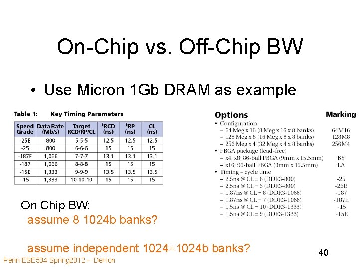
On-Chip vs. Off-Chip BW • Use Micron 1 Gb DRAM as example On Chip BW: assume 8 1024 b banks? assume independent 1024× 1024 b banks? Penn ESE 534 Spring 2012 -- De. Hon 40
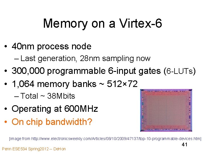
Memory on a Virtex-6 • 40 nm process node – Last generation, 28 nm sampling now • 300, 000 programmable 6 -input gates (6 -LUTs) • 1, 064 memory banks ~ 512× 72 – Total ~ 38 Mbits • Operating at 600 MHz • On chip bandwidth? [image from http: //www. electronicsweekly. com/Articles/08/10/2009/47137/top-10 -programmable-devices. htm] Penn ESE 534 Spring 2012 -- De. Hon 41
Costs Change • Design space changes when whole system goes on single chip • Can afford – wider busses – more banks – memory tailored to application/architecture • Beware of old (stale) answers – their cost model was different Penn ESE 534 Spring 2012 -- De. Hon 42
What is Importance of Memory? • Radical Hypothesis: – Memory is simply a very efficient organization which allows us to store data compactly • (at least, in the technologies we’ve seen to date) – A great engineering trick to optimize resources • Alternative: – memory is a primary • State is a primary, but state≠memory Penn ESE 534 Spring 2012 -- De. Hon 43
Admin • HW 1 and 2 graded – note feedback (even if received perfect score) • HW 4 out today • Reading – Was for today – Nothing new for Wed. , Mon. • Office Hours: Tuesday 4: 15 pm Penn ESE 534 Spring 2012 -- De. Hon 44
Big Ideas [MSB Ideas] • Memory: efficient way to hold state • Resource sharing: key trick to reduce area • Memories are a great example of resource sharing Penn ESE 534 Spring 2012 -- De. Hon 45
Big Ideas [MSB-1 Ideas] • Tradeoffs in memory organization • Changing cost of memory organization as we go to on-chip, embedded memories Penn ESE 534 Spring 2012 -- De. Hon 46
- Slides: 46