ESE 370 CircuitLevel Modeling Design and Optimization for
- Slides: 30

ESE 370: Circuit-Level Modeling, Design, and Optimization for Digital Systems Day 24: November 5, 2010 Memory Overview Penn ESE 370 Fall 2010 -- De. Hon 1

Today • Memory – Motivation – Organization – Basic components – Optimization concerns Penn ESE 370 Fall 2010 -- De. Hon 2

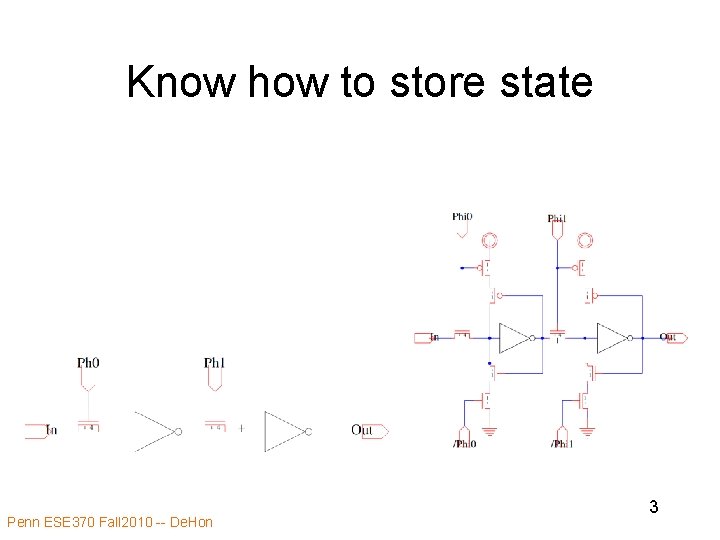
Know how to store state Penn ESE 370 Fall 2010 -- De. Hon 3

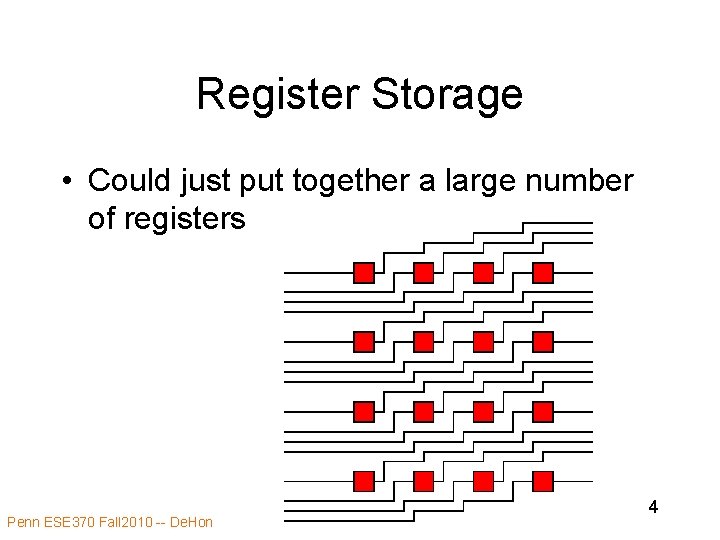
Register Storage • Could just put together a large number of registers Penn ESE 370 Fall 2010 -- De. Hon 4

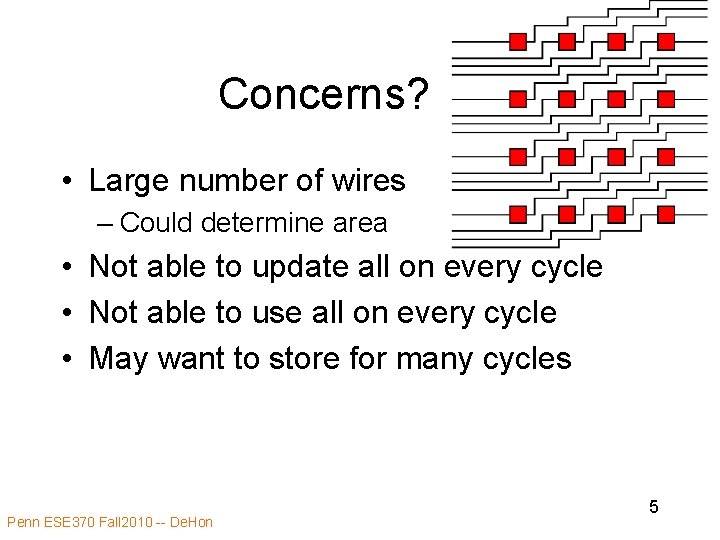
Concerns? • Large number of wires – Could determine area • Not able to update all on every cycle • Not able to use all on every cycle • May want to store for many cycles Penn ESE 370 Fall 2010 -- De. Hon 5

Limited Data Use • What if can only use on each cycle? – Use with shared data path • Need to select the one output – Can only update one • Need to control which one gets written Penn ESE 370 Fall 2010 -- De. Hon 6

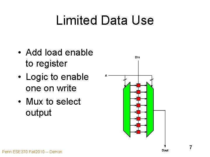
Limited Data Use • Add load enable to register • Logic to enable on write • Mux to select output Penn ESE 370 Fall 2010 -- De. Hon 7

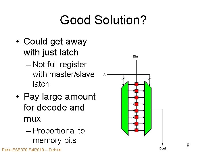
Good Solution? • Could get away with just latch – Not full register with master/slave latch • Pay large amount for decode and mux – Proportional to memory bits Penn ESE 370 Fall 2010 -- De. Hon 8

Memory Idea • Maximize storage density (bits/cm 2) • By minimizing the size/complexity of the repeated element • Use shared periphery circuits to provide full functionality • Trades off bandwidth (concurrent access) to save area Penn ESE 370 Fall 2010 -- De. Hon 9

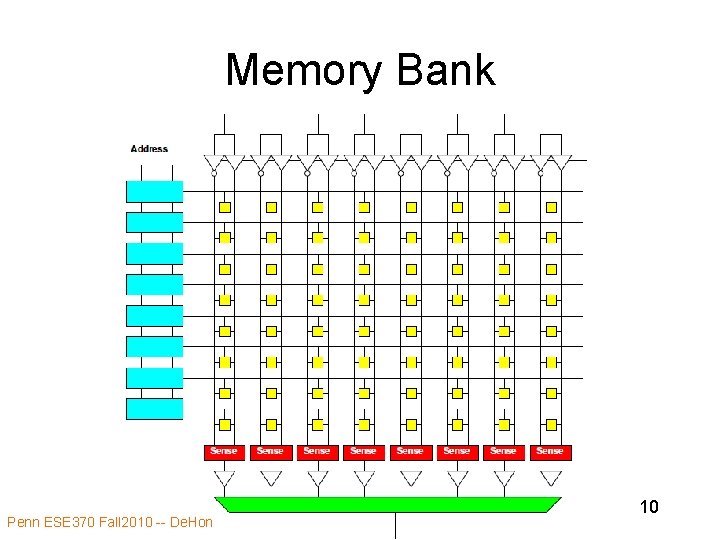
Memory Bank Penn ESE 370 Fall 2010 -- De. Hon 10

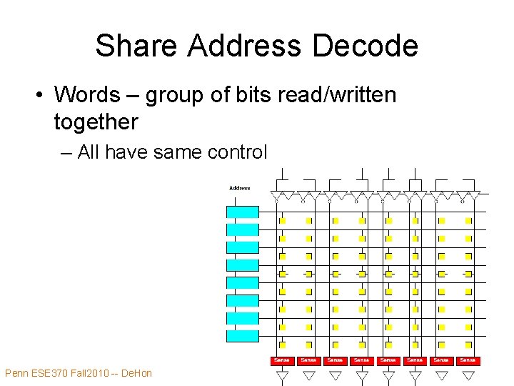
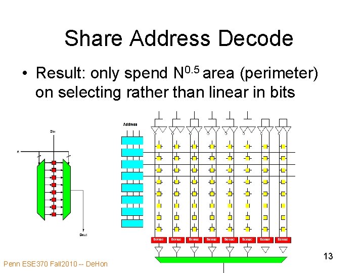
Share Address Decode • Words – group of bits read/written together – All have same control Penn ESE 370 Fall 2010 -- De. Hon 11

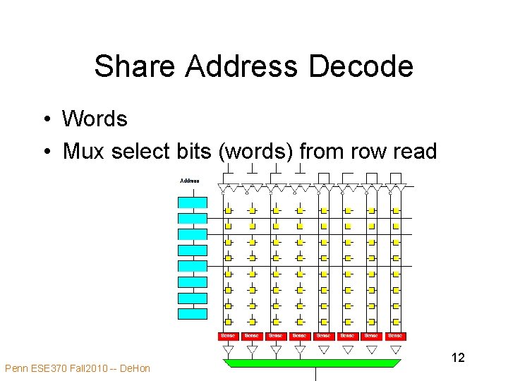
Share Address Decode • Words • Mux select bits (words) from row read Penn ESE 370 Fall 2010 -- De. Hon 12

Share Address Decode • Result: only spend N 0. 5 area (perimeter) on selecting rather than linear in bits Penn ESE 370 Fall 2010 -- De. Hon 13

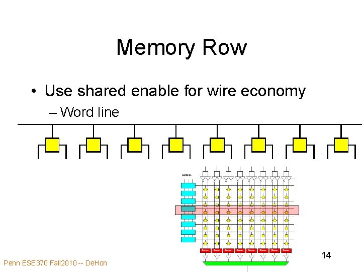
Memory Row • Use shared enable for wire economy – Word line Penn ESE 370 Fall 2010 -- De. Hon 14

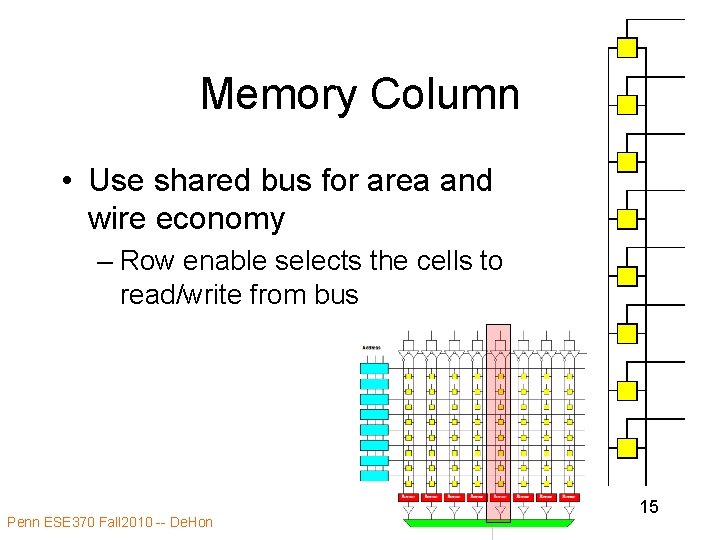
Memory Column • Use shared bus for area and wire economy – Row enable selects the cells to read/write from bus Penn ESE 370 Fall 2010 -- De. Hon 15

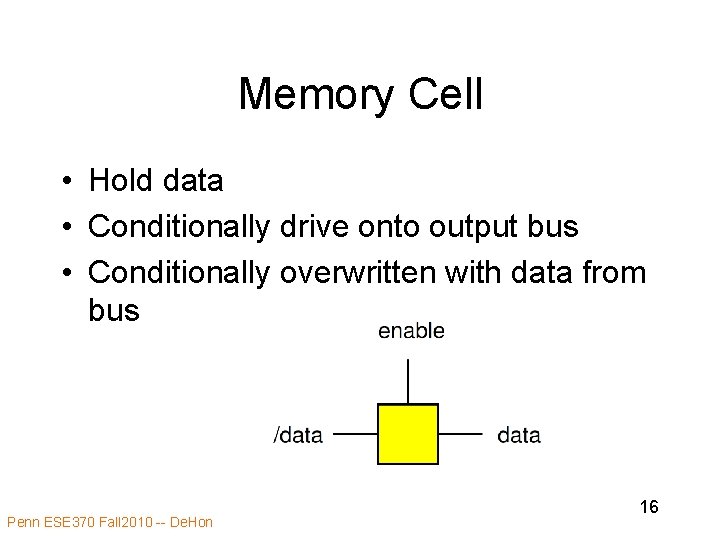
Memory Cell • Hold data • Conditionally drive onto output bus • Conditionally overwritten with data from bus Penn ESE 370 Fall 2010 -- De. Hon 16

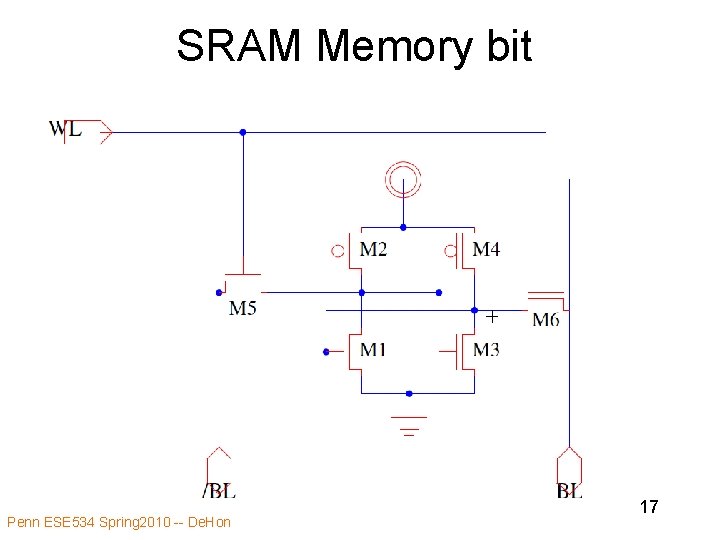
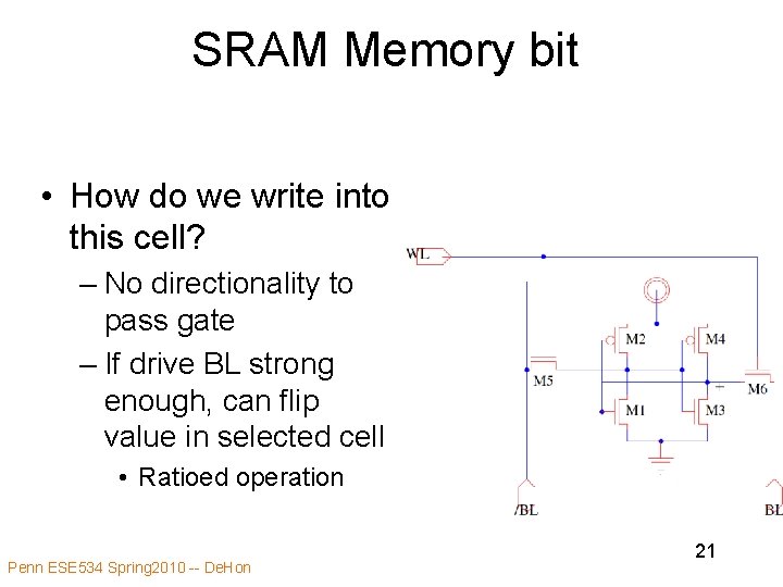
SRAM Memory bit Penn ESE 534 Spring 2010 -- De. Hon 17

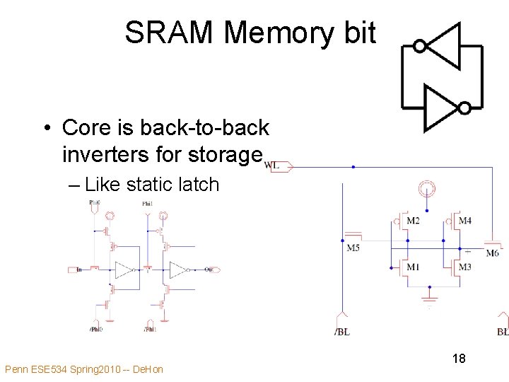
SRAM Memory bit • Core is back-to-back inverters for storage – Like static latch Penn ESE 534 Spring 2010 -- De. Hon 18

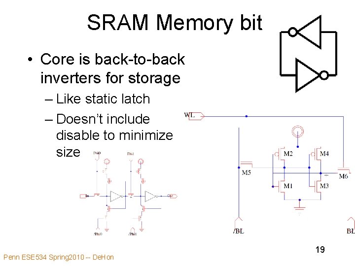
SRAM Memory bit • Core is back-to-back inverters for storage – Like static latch – Doesn’t include disable to minimize size Penn ESE 534 Spring 2010 -- De. Hon 19

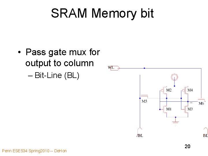
SRAM Memory bit • Pass gate mux for output to column – Bit-Line (BL) Penn ESE 534 Spring 2010 -- De. Hon 20

SRAM Memory bit • How do we write into this cell? – No directionality to pass gate – If drive BL strong enough, can flip value in selected cell • Ratioed operation Penn ESE 534 Spring 2010 -- De. Hon 21

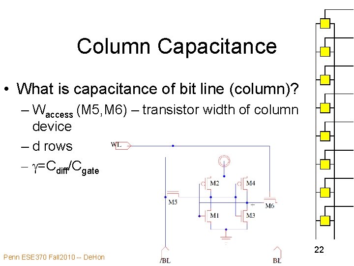
Column Capacitance • What is capacitance of bit line (column)? – Waccess (M 5, M 6) – transistor width of column device – d rows – g=Cdiff/Cgate Penn ESE 370 Fall 2010 -- De. Hon 22

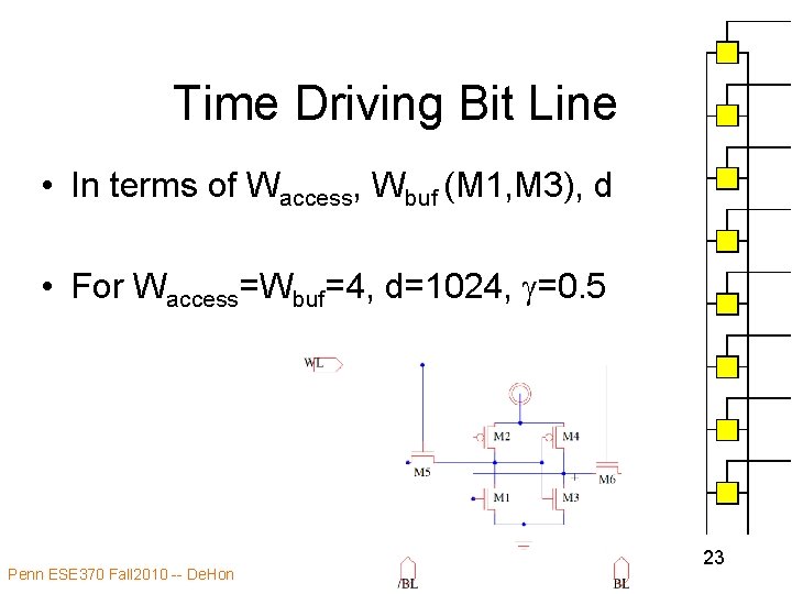
Time Driving Bit Line • In terms of Waccess, Wbuf (M 1, M 3), d • For Waccess=Wbuf=4, d=1024, g=0. 5 Penn ESE 370 Fall 2010 -- De. Hon 23

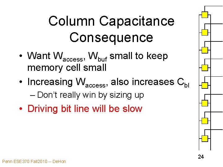
Column Capacitance Consequence • Want Waccess, Wbuf small to keep memory cell small • Increasing Waccess, also increases Cbl – Don’t really win by sizing up • Driving bit line will be slow Penn ESE 370 Fall 2010 -- De. Hon 24

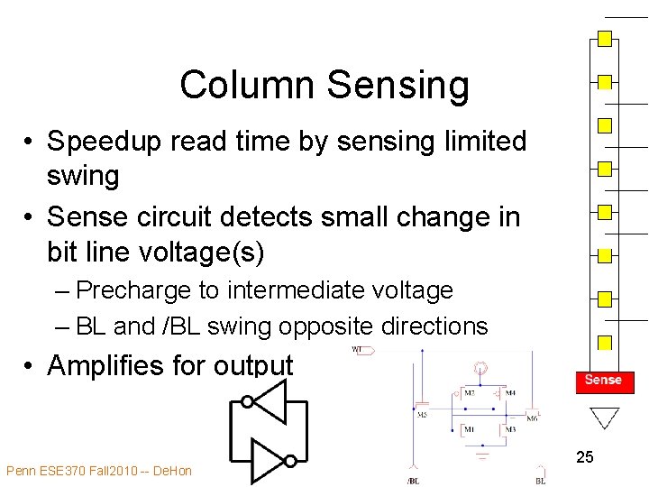
Column Sensing • Speedup read time by sensing limited swing • Sense circuit detects small change in bit line voltage(s) – Precharge to intermediate voltage – BL and /BL swing opposite directions • Amplifies for output Penn ESE 370 Fall 2010 -- De. Hon 25

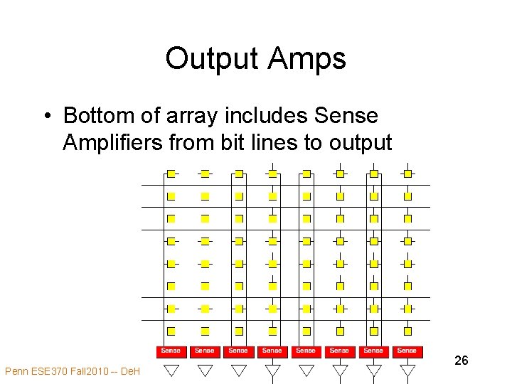
Output Amps • Bottom of array includes Sense Amplifiers from bit lines to output Penn ESE 370 Fall 2010 -- De. Hon 26

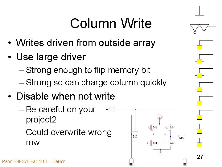
Column Write • Writes driven from outside array • Use large driver – Strong enough to flip memory bit – Strong so can charge column quickly • Disable when not write – Be careful on your project 2 – Could overwrite wrong row Penn ESE 370 Fall 2010 -- De. Hon 27

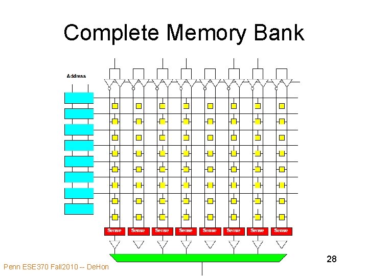
Complete Memory Bank Penn ESE 370 Fall 2010 -- De. Hon 28

Admin • Project 2 out – Due November 17 • Note recommend milestones • Time change this weekend (Sunday 2 am) – Extra hour to work on project? • Next week normal – Lectures MWF – Office hours Penn ESE 370 Fall 2010 -- De. Hon 29

Idea • Memory for compact state storage • Share circuitry across many bits – Minimize area per bit maximize density • Aggressively use: – Pass transistors, Ratioing – Precharge, Amplifiers to keep area down Penn ESE 370 Fall 2010 -- De. Hon 30