ESE 370 CircuitLevel Modeling Design and Optimization for

- Slides: 43

ESE 370: Circuit-Level Modeling, Design, and Optimization for Digital Systems Day 3: September 12, 2011 Transistor Introduction (first order) Penn ESE 370 Fall 2011 -- De. Hon 1

Today • First order model • There always Rs and Cs Penn ESE 370 Fall 2011 -- De. Hon 2

Last Time • Quasi-Static – inputs transition, circuit responds, and settles – Dynamic transition to roughly static states • DC/Steady-State – Ignore the capacitors • Zeroth-order allows us to reason (mostly) at logic level about steady-state functionality of typical gate circuits Penn ESE 370 Fall 2011 -- De. Hon 3

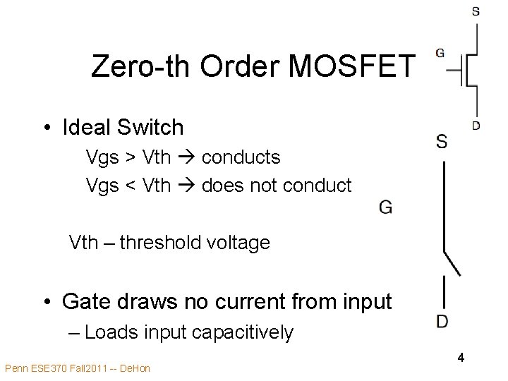
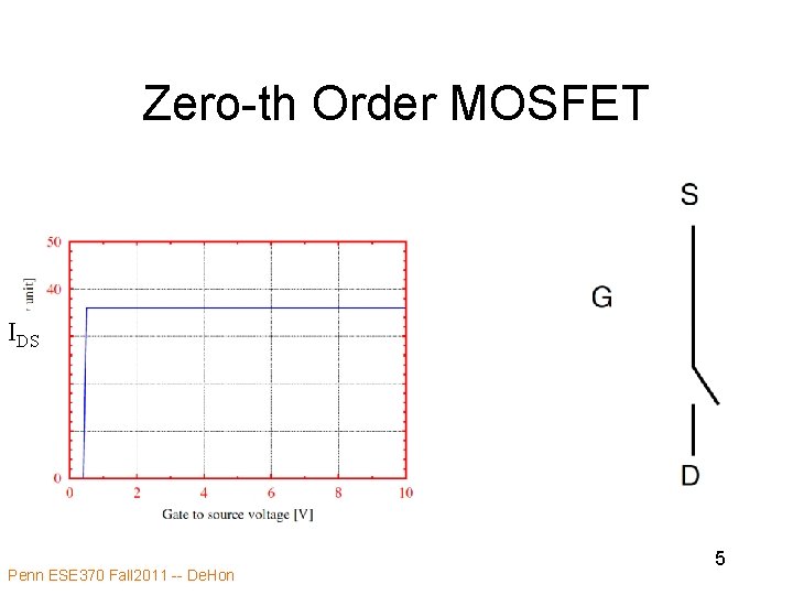
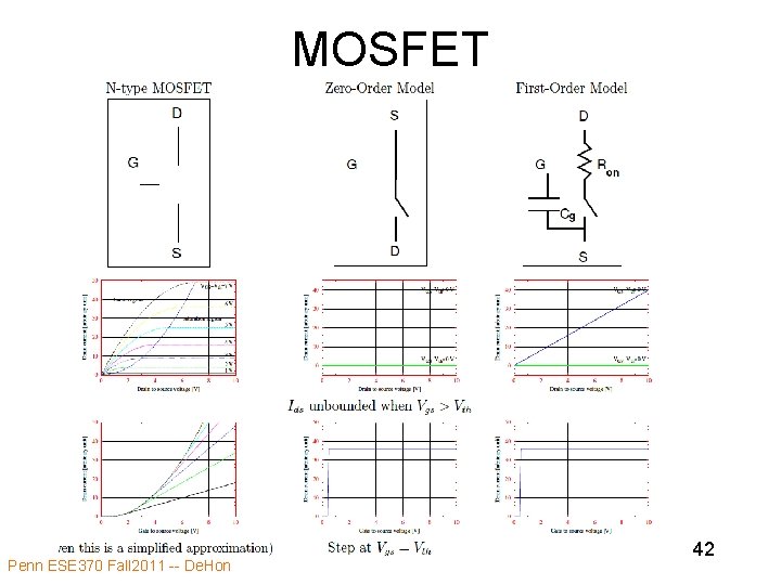
Zero-th Order MOSFET • Ideal Switch Vgs > Vth conducts Vgs < Vth does not conduct Vth – threshold voltage • Gate draws no current from input – Loads input capacitively Penn ESE 370 Fall 2011 -- De. Hon 4

Zero-th Order MOSFET IDS Penn ESE 370 Fall 2011 -- De. Hon 5

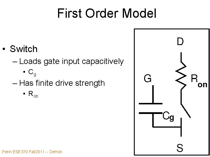
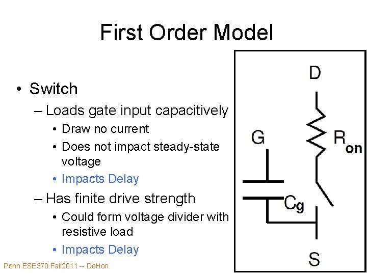
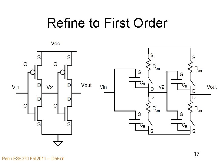
First Order Model • Switch – Loads gate input capacitively • Cg – Has finite drive strength • Ron Penn ESE 370 Fall 2011 -- De. Hon 6

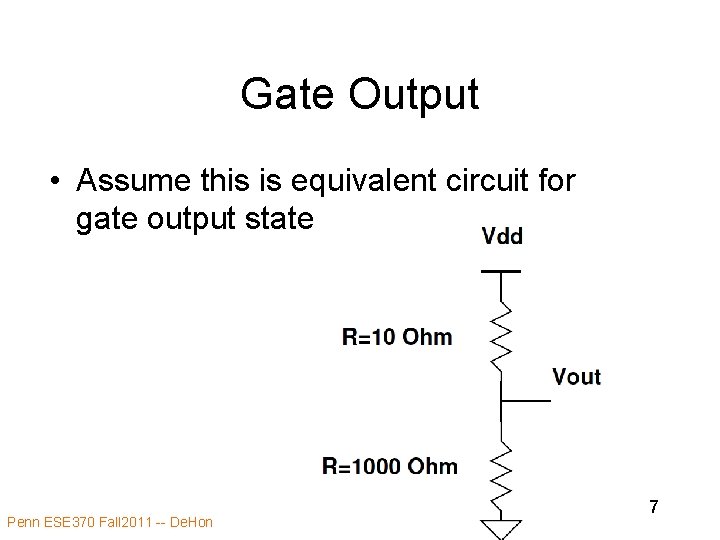
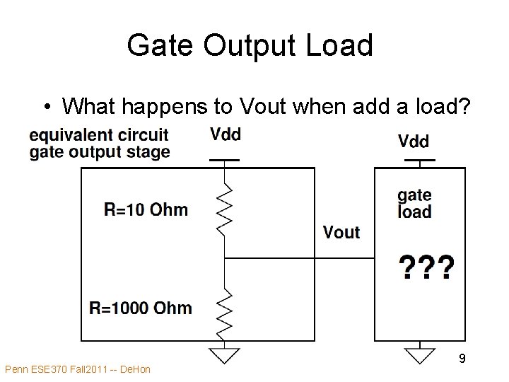
Gate Output • Assume this is equivalent circuit for gate output state Penn ESE 370 Fall 2011 -- De. Hon 7

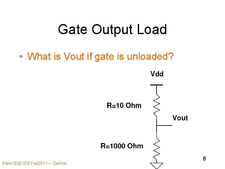
Gate Output Load • What is Vout if gate is unloaded? Penn ESE 370 Fall 2011 -- De. Hon 8

Gate Output Load • What happens to Vout when add a load? Penn ESE 370 Fall 2011 -- De. Hon 9

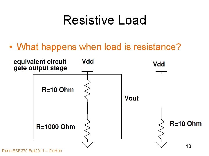
Resistive Load • What happens when load is resistance? Penn ESE 370 Fall 2011 -- De. Hon 10

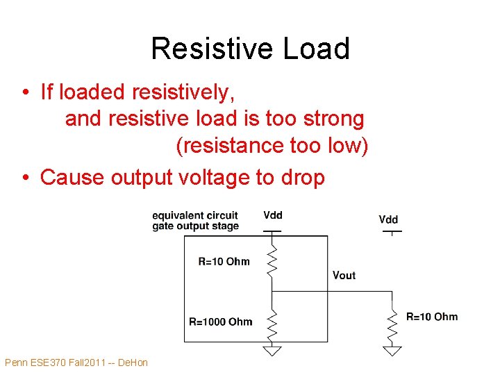
Resistive Load • If loaded resistively, and resistive load is too strong (resistance too low) • Cause output voltage to drop Penn ESE 370 Fall 2011 -- De. Hon 11

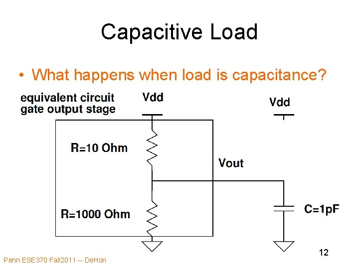
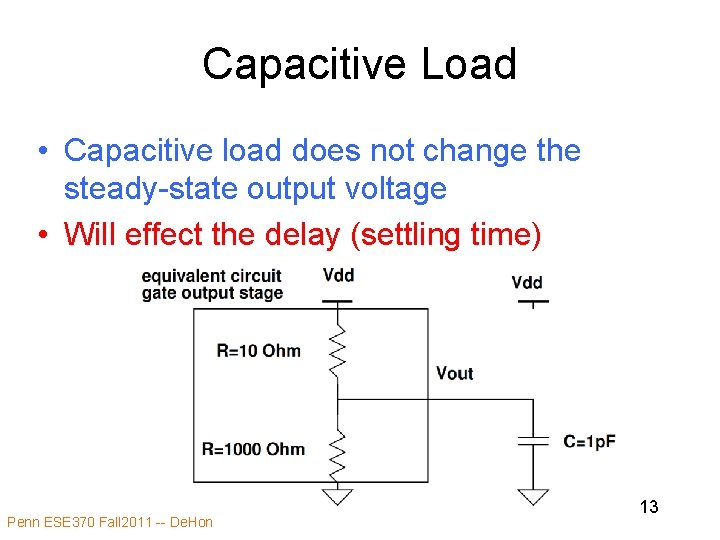
Capacitive Load • What happens when load is capacitance? Penn ESE 370 Fall 2011 -- De. Hon 12

Capacitive Load • Capacitive load does not change the steady-state output voltage • Will effect the delay (settling time) Penn ESE 370 Fall 2011 -- De. Hon 13

First Order Model • Switch – Loads gate input capacitively • Draw no current • Does not impact steady-state voltage • Impacts Delay – Has finite drive strength • Could form voltage divider with resistive load • Impacts Delay Penn ESE 370 Fall 2011 -- De. Hon 14

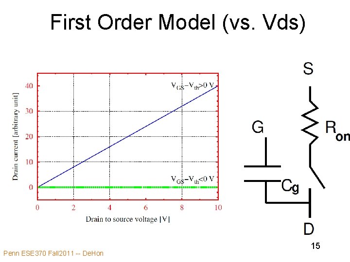
First Order Model (vs. Vds) Penn ESE 370 Fall 2011 -- De. Hon 15

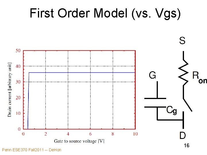
First Order Model (vs. Vgs) Penn ESE 370 Fall 2011 -- De. Hon 16

Refine to First Order Penn ESE 370 Fall 2011 -- De. Hon 17

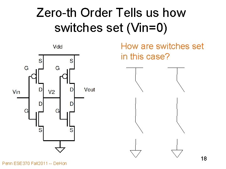
Zero-th Order Tells us how switches set (Vin=0) How are switches set in this case? Penn ESE 370 Fall 2011 -- De. Hon 18

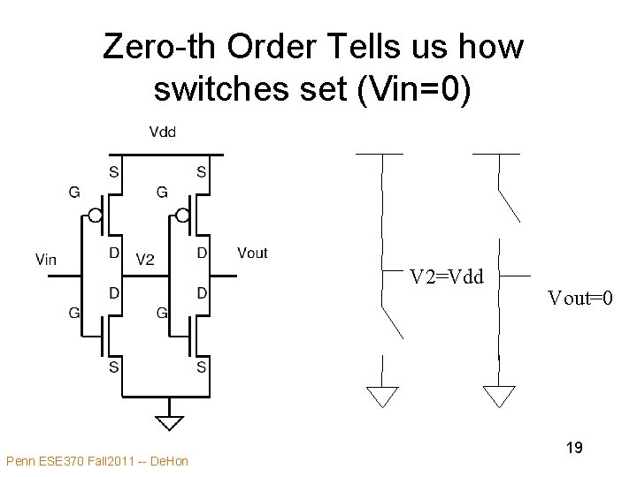
Zero-th Order Tells us how switches set (Vin=0) V 2=Vdd Penn ESE 370 Fall 2011 -- De. Hon Vout=0 19

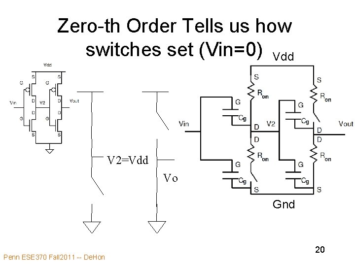
Zero-th Order Tells us how switches set (Vin=0) Vdd V 2=Vdd Vout=0 Gnd Penn ESE 370 Fall 2011 -- De. Hon 20

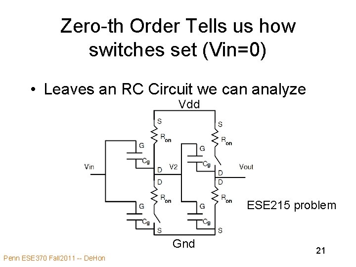
Zero-th Order Tells us how switches set (Vin=0) • Leaves an RC Circuit we can analyze Vdd ESE 215 problem Gnd Penn ESE 370 Fall 2011 -- De. Hon 21

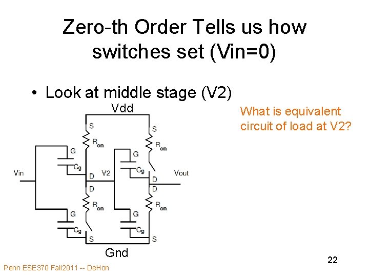
Zero-th Order Tells us how switches set (Vin=0) • Look at middle stage (V 2) Vdd Gnd Penn ESE 370 Fall 2011 -- De. Hon What is equivalent circuit of load at V 2? 22

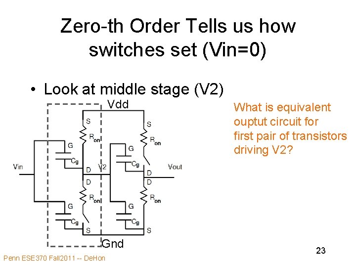
Zero-th Order Tells us how switches set (Vin=0) • Look at middle stage (V 2) Vdd Gnd Penn ESE 370 Fall 2011 -- De. Hon What is equivalent ouptut circuit for first pair of transistors driving V 2? 23

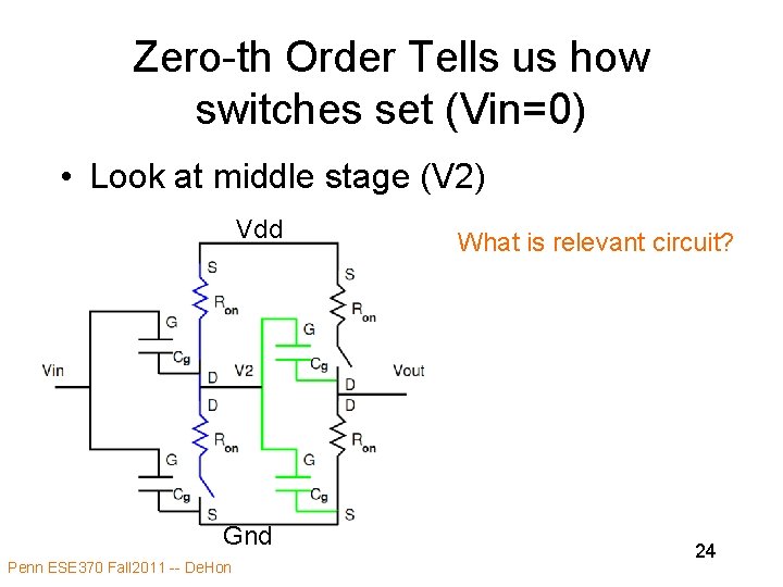
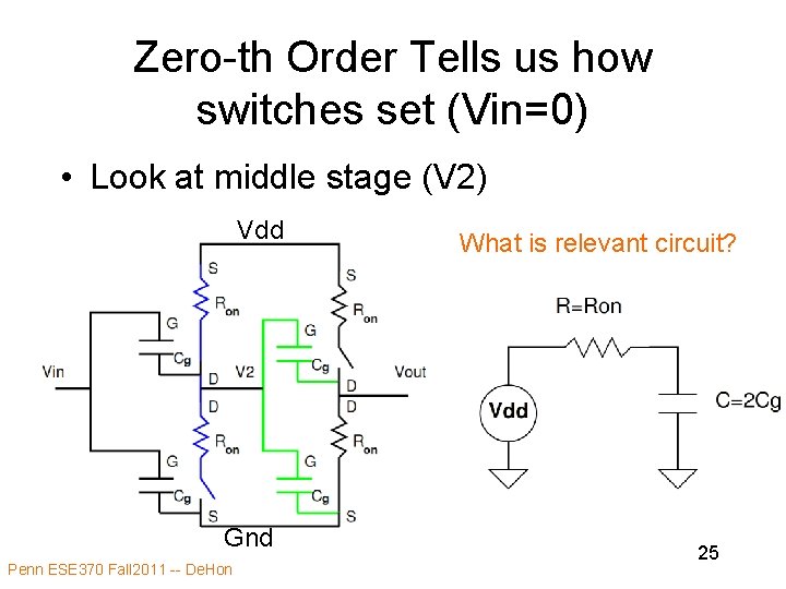
Zero-th Order Tells us how switches set (Vin=0) • Look at middle stage (V 2) Vdd Gnd Penn ESE 370 Fall 2011 -- De. Hon What is relevant circuit? 24

Zero-th Order Tells us how switches set (Vin=0) • Look at middle stage (V 2) Vdd Gnd Penn ESE 370 Fall 2011 -- De. Hon What is relevant circuit? 25

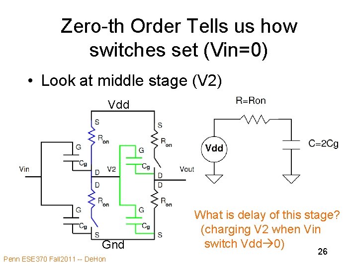
Zero-th Order Tells us how switches set (Vin=0) • Look at middle stage (V 2) Vdd Gnd Penn ESE 370 Fall 2011 -- De. Hon What is delay of this stage? (charging V 2 when Vin switch Vdd 0) 26

What more does first-order model tell us? • Delay • Quastistatic behavior • Voltage settling with resistive loads – At least some basis for reasoning Penn ESE 370 Fall 2011 -- De. Hon 27

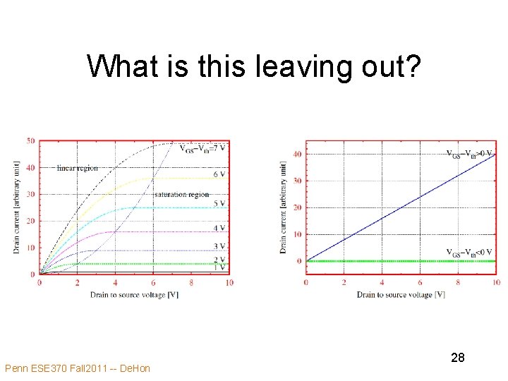
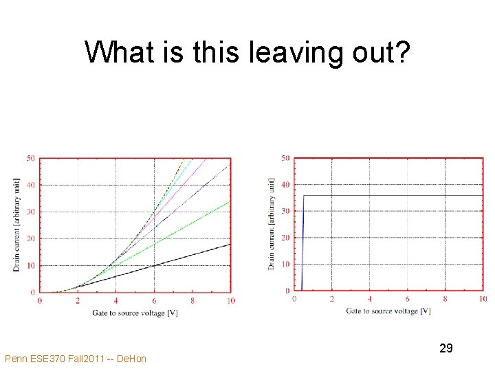
What is this leaving out? Penn ESE 370 Fall 2011 -- De. Hon 28

What is this leaving out? Penn ESE 370 Fall 2011 -- De. Hon 29

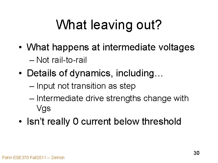
What leaving out? • What happens at intermediate voltages – Not rail-to-rail • Details of dynamics, including… – Input not transition as step – Intermediate drive strengths change with Vgs • Isn’t really 0 current below threshold Penn ESE 370 Fall 2011 -- De. Hon 30

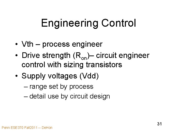
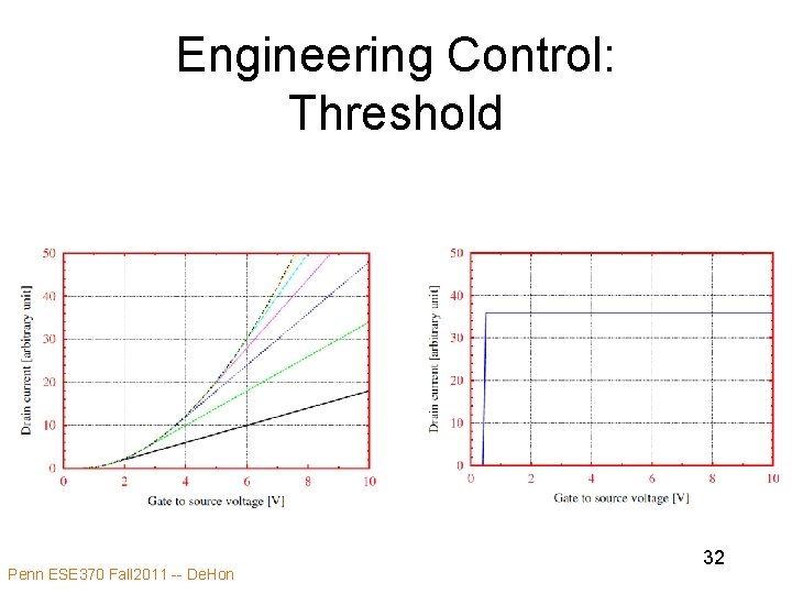
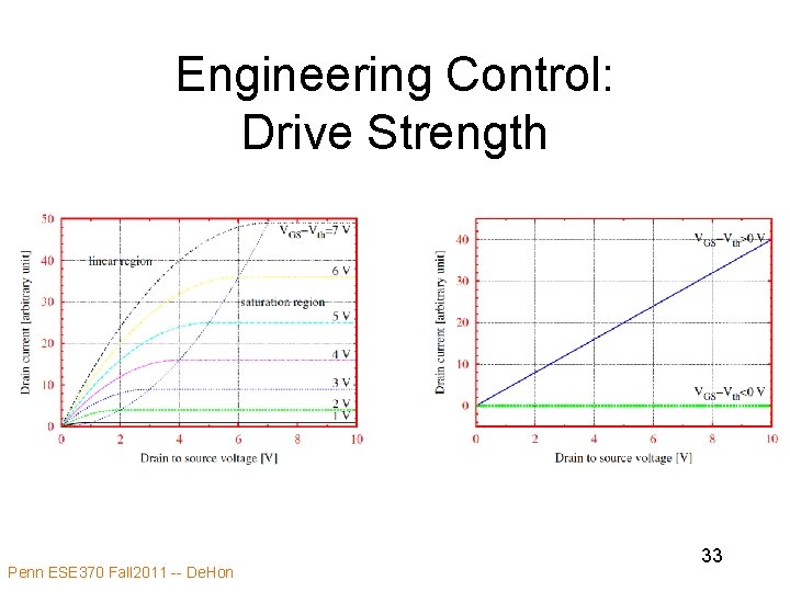
Engineering Control • Vth – process engineer • Drive strength (Ron)– circuit engineer control with sizing transistors • Supply voltages (Vdd) – range set by process – detail use by circuit design Penn ESE 370 Fall 2011 -- De. Hon 31

Engineering Control: Threshold Penn ESE 370 Fall 2011 -- De. Hon 32

Engineering Control: Drive Strength Penn ESE 370 Fall 2011 -- De. Hon 33

Rs and Cs Penn ESE 370 Fall 2011 -- De. Hon 34

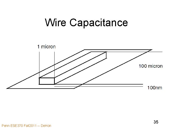
Wire Capacitance Penn ESE 370 Fall 2011 -- De. Hon 35

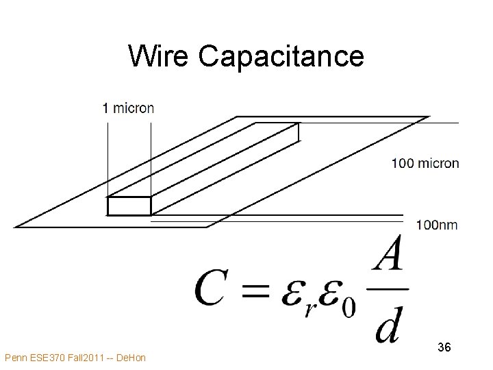
Wire Capacitance Penn ESE 370 Fall 2011 -- De. Hon 36

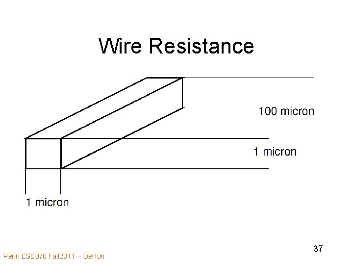
Wire Resistance Penn ESE 370 Fall 2011 -- De. Hon 37

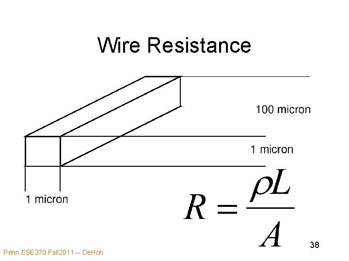
Wire Resistance Penn ESE 370 Fall 2011 -- De. Hon 38

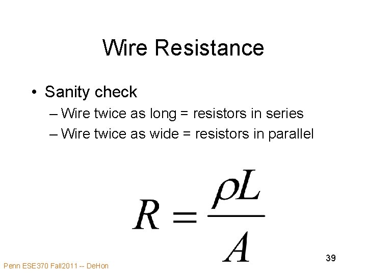
Wire Resistance • Sanity check – Wire twice as long = resistors in series – Wire twice as wide = resistors in parallel Penn ESE 370 Fall 2011 -- De. Hon 39

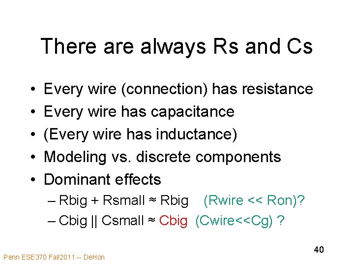
There always Rs and Cs • • • Every wire (connection) has resistance Every wire has capacitance (Every wire has inductance) Modeling vs. discrete components Dominant effects – Rbig + Rsmall ≈ Rbig (Rwire << Ron)? – Cbig || Csmall ≈ Cbig (Cwire<<Cg) ? Penn ESE 370 Fall 2011 -- De. Hon 40

Admin • TA: Paul Gurniak – Email: pgurniak seas – Office Hours: W 3 -4 pm, R 1: 30 -2: 30 pm • Ketterer • André office hours: T 4: 00 pm • Lecture Wednesday: building gates – Reading • Lab on Friday – Homework due, bring USB drive Penn ESE 370 Fall 2011 -- De. Hon 41

MOSFET Penn ESE 370 Fall 2011 -- De. Hon 42

Big Ideas • MOSFET Transistor as switch • Purpose-driven simplified modeling – Aid reasoning, sanity check, simplify design • Analysis methodology – zero-th order to understand switch state (logic) – First-order to get equivalent RC circuit (delay) • New perspective on Rs and Cs Penn ESE 370 Fall 2011 -- De. Hon 43