
ESE 370 CircuitLevel Modeling Design and Optimization for
- Slides: 49
ESE 370: Circuit-Level Modeling, Design, and Optimization for Digital Systems Day 27: November 14, 2011 Memory Core Penn ESE 370 Fall 2011 -- De. Hon 1
Today • 6 T SRAM review • 5 T SRAM – Charge sharing – Precharge • DRAM • Leakage • Multiport SRAM (time permitting) Penn ESE 370 Fall 2011 -- De. Hon 2
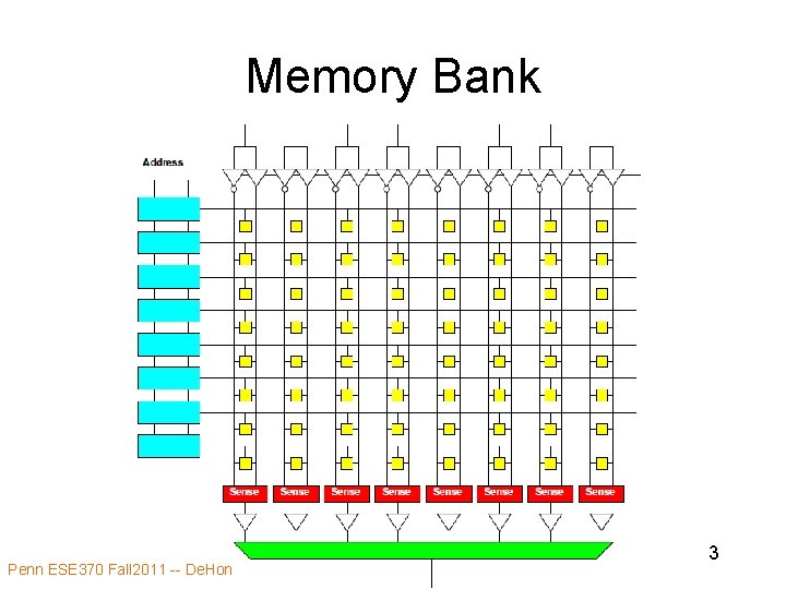
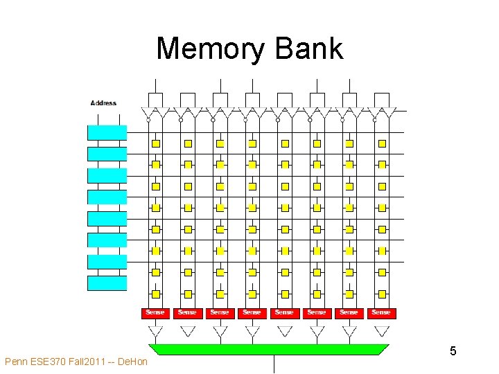
Memory Bank Penn ESE 370 Fall 2011 -- De. Hon 3
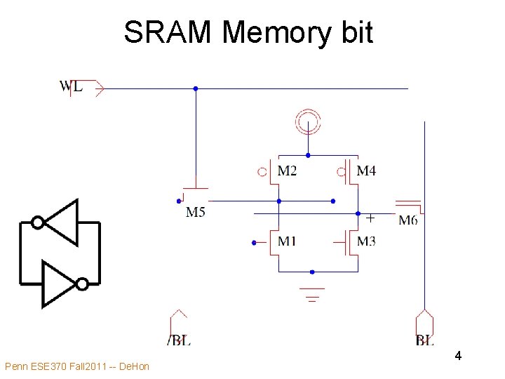
SRAM Memory bit Penn ESE 370 Fall 2011 -- De. Hon 4
Memory Bank Penn ESE 370 Fall 2011 -- De. Hon 5
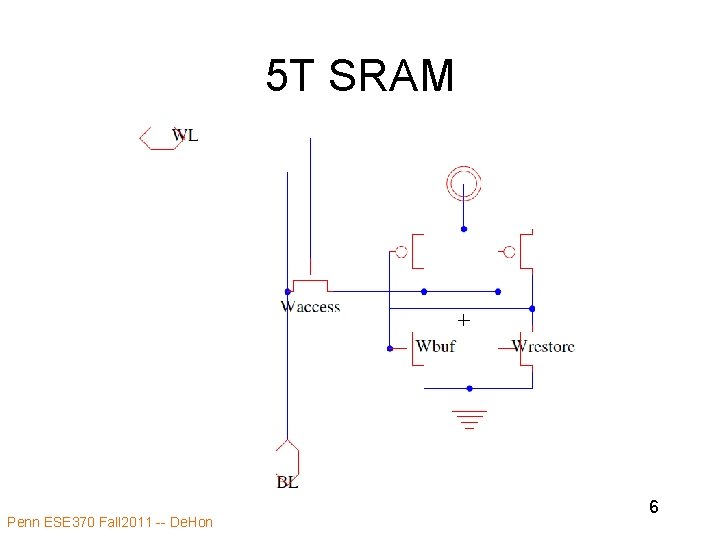
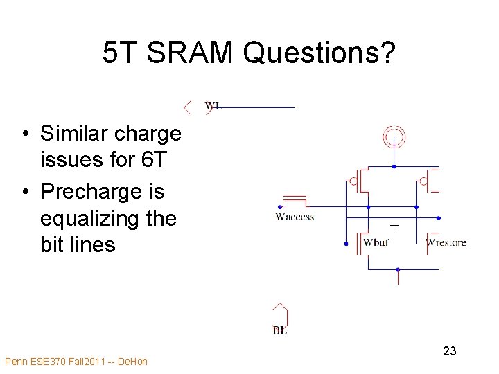
5 T SRAM Penn ESE 370 Fall 2011 -- De. Hon 6
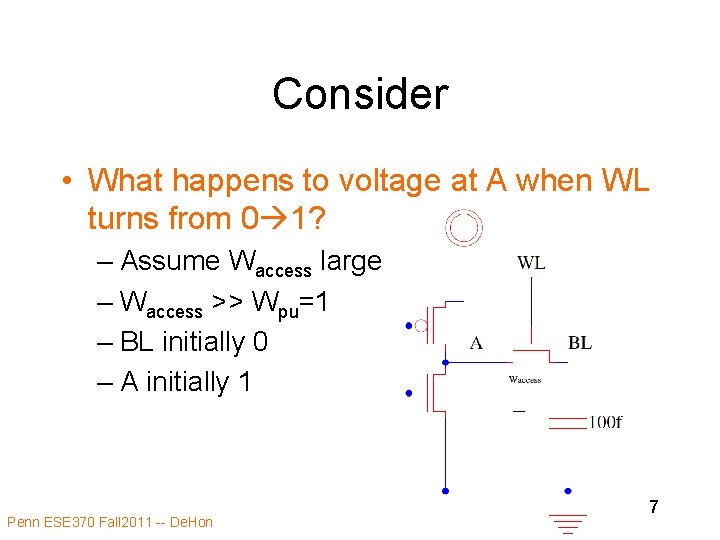
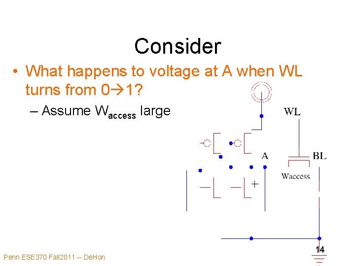
Consider • What happens to voltage at A when WL turns from 0 1? – Assume Waccess large – Waccess >> Wpu=1 – BL initially 0 – A initially 1 Penn ESE 370 Fall 2011 -- De. Hon 7
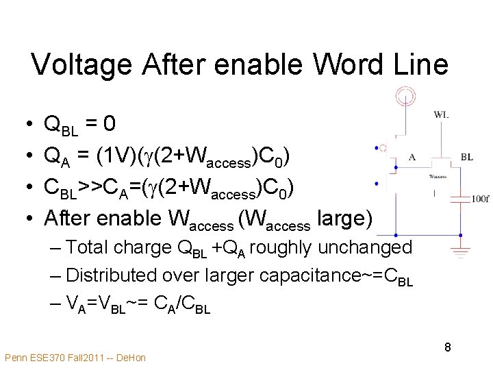
Voltage After enable Word Line • • QBL = 0 QA = (1 V)(g(2+Waccess)C 0) CBL>>CA=(g(2+Waccess)C 0) After enable Waccess (Waccess large) – Total charge QBL +QA roughly unchanged – Distributed over larger capacitance~=CBL – VA=VBL~= CA/CBL Penn ESE 370 Fall 2011 -- De. Hon 8
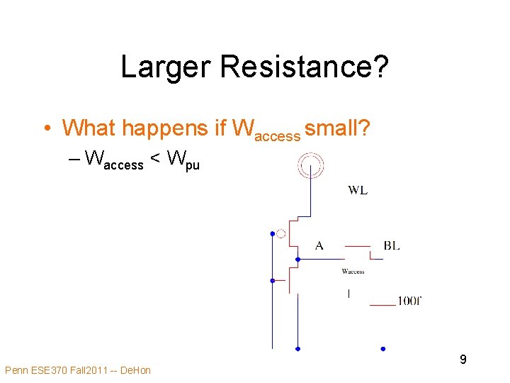
Larger Resistance? • What happens if Waccess small? – Waccess < Wpu Penn ESE 370 Fall 2011 -- De. Hon 9
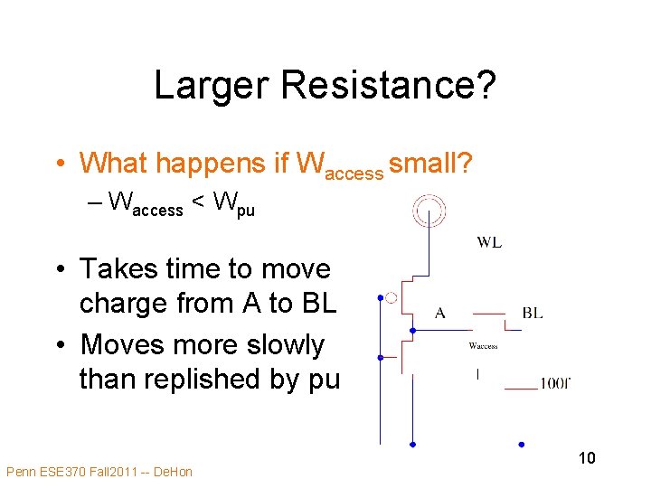
Larger Resistance? • What happens if Waccess small? – Waccess < Wpu • Takes time to move charge from A to BL • Moves more slowly than replished by pu Penn ESE 370 Fall 2011 -- De. Hon 10
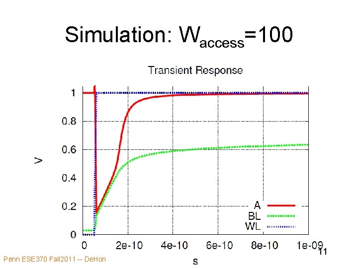
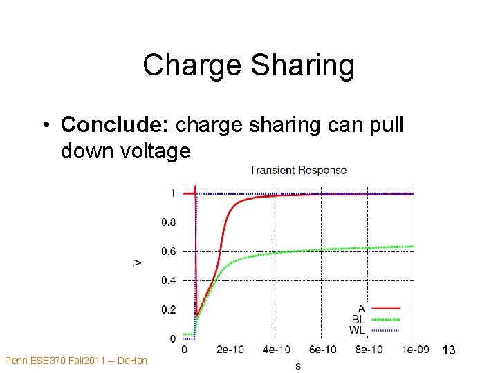
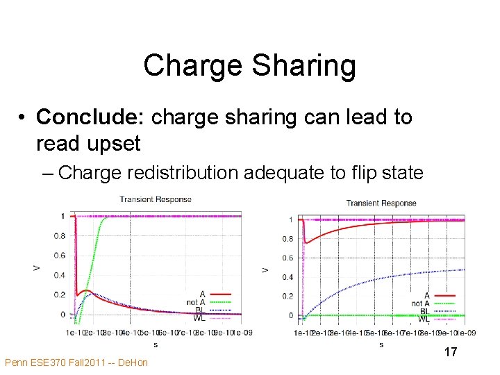
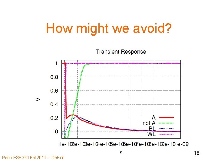
Simulation: Waccess=100 Penn ESE 370 Fall 2011 -- De. Hon 11
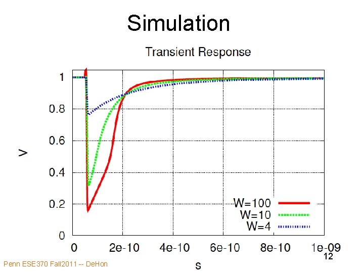
Simulation Penn ESE 370 Fall 2011 -- De. Hon 12
Charge Sharing • Conclude: charge sharing can pull down voltage Penn ESE 370 Fall 2011 -- De. Hon 13
Consider • What happens to voltage at A when WL turns from 0 1? – Assume Waccess large Penn ESE 370 Fall 2011 -- De. Hon 14
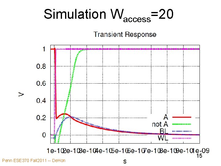
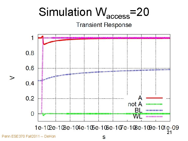
Simulation Waccess=20 Penn ESE 370 Fall 2011 -- De. Hon 15
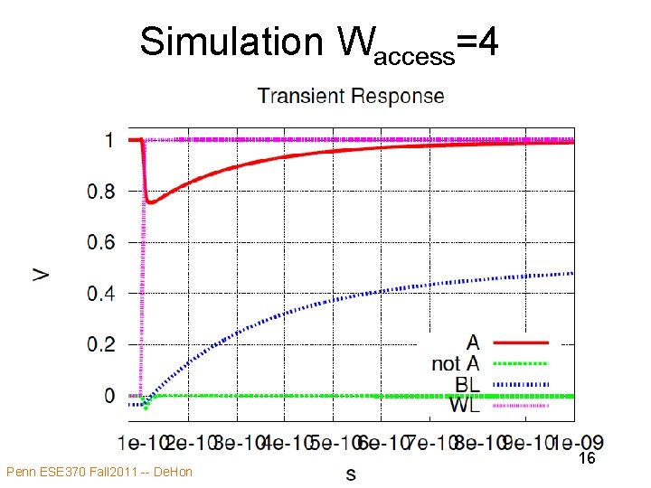
Simulation Waccess=4 Penn ESE 370 Fall 2011 -- De. Hon 16
Charge Sharing • Conclude: charge sharing can lead to read upset – Charge redistribution adequate to flip state of bit Penn ESE 370 Fall 2011 -- De. Hon 17
How might we avoid? Penn ESE 370 Fall 2011 -- De. Hon 18
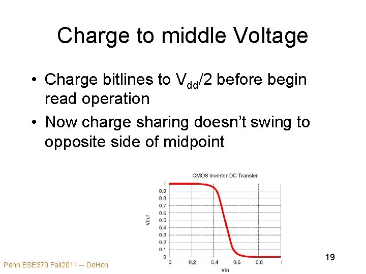
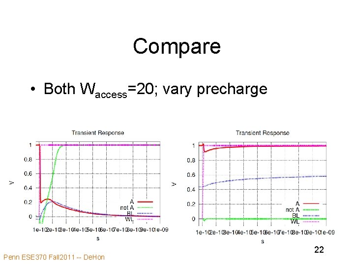
Charge to middle Voltage • Charge bitlines to Vdd/2 before begin read operation • Now charge sharing doesn’t swing to opposite side of midpoint Penn ESE 370 Fall 2011 -- De. Hon 19
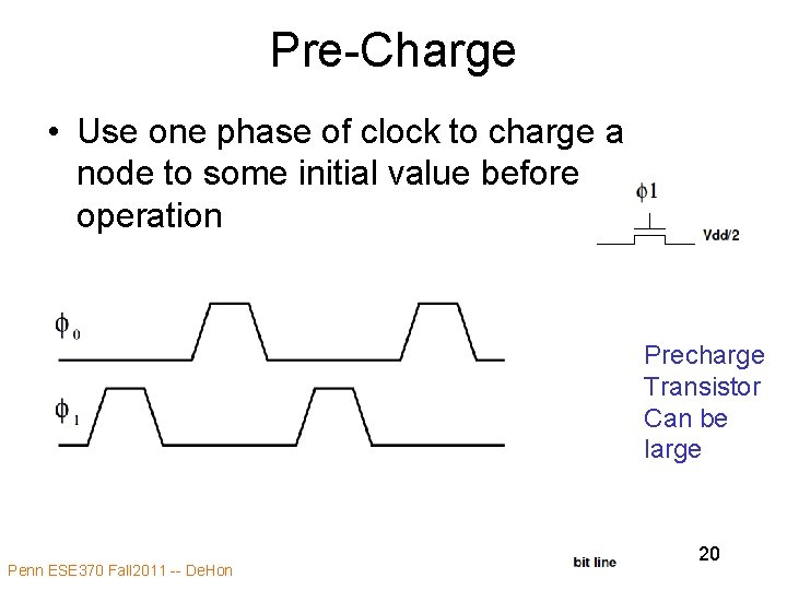
Pre-Charge • Use one phase of clock to charge a node to some initial value before operation Precharge Transistor Can be large Penn ESE 370 Fall 2011 -- De. Hon 20
Simulation Waccess=20 Penn ESE 370 Fall 2011 -- De. Hon 21
Compare • Both Waccess=20; vary precharge Penn ESE 370 Fall 2011 -- De. Hon 22
5 T SRAM Questions? • Similar charge issues for 6 T • Precharge is equalizing the bit lines Penn ESE 370 Fall 2011 -- De. Hon 23
DRAM Penn ESE 370 Fall 2011 -- De. Hon 24
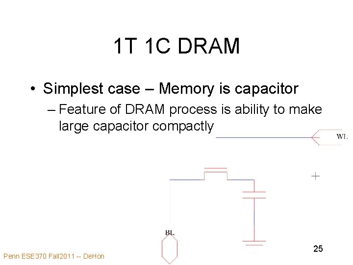
1 T 1 C DRAM • Simplest case – Memory is capacitor – Feature of DRAM process is ability to make large capacitor compactly Penn ESE 370 Fall 2011 -- De. Hon 25
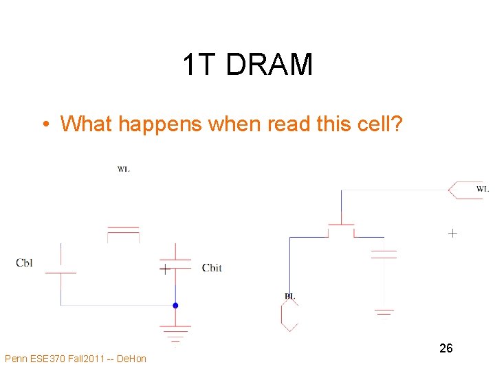
1 T DRAM • What happens when read this cell? Penn ESE 370 Fall 2011 -- De. Hon 26
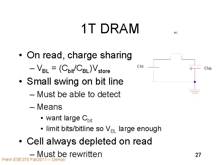
1 T DRAM • On read, charge sharing – VBL = (Cbit/CBL)Vstore • Small swing on bit line – Must be able to detect – Means • want large Cbit • limit bits/bitline so VBL large enough • Cell always depleted on read – Must be rewritten Penn ESE 370 Fall 2011 -- De. Hon 27
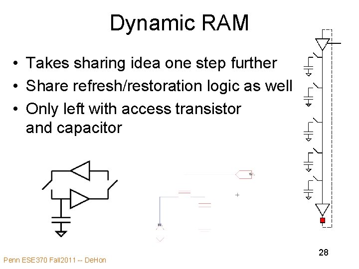
Dynamic RAM • Takes sharing idea one step further • Share refresh/restoration logic as well • Only left with access transistor and capacitor Penn ESE 370 Fall 2011 -- De. Hon 28
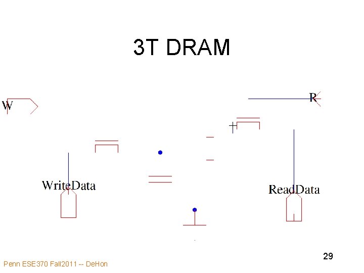
3 T DRAM Penn ESE 370 Fall 2011 -- De. Hon 29
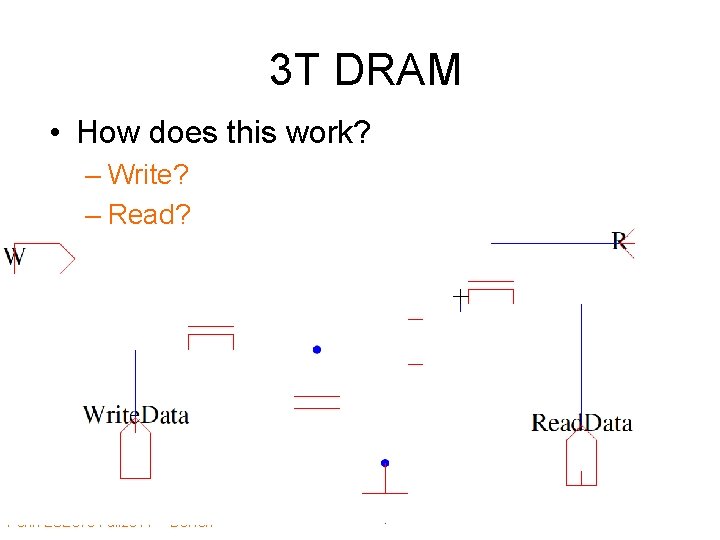
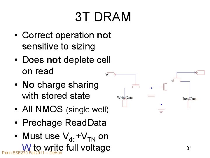
3 T DRAM • How does this work? – Write? – Read? Penn ESE 370 Fall 2011 -- De. Hon 30
3 T DRAM • Correct operation not sensitive to sizing • Does not deplete cell on read • No charge sharing with stored state • All NMOS (single well) • Prechage Read. Data • Must use Vdd+VTN on W to write full voltage Penn ESE 370 Fall 2011 -- De. Hon 31
Some Numbers (memory) • Register as stand-alone element (14 T) 4 Kl 2 • Static RAM cell (6 T) 1 Kl 2 – SRAM Memory (single ported) • Dynamic RAM cell (DRAM process) 100 l 2 • Dynamic RAM cell (SRAM process) 300 l 2 Penn ESE 370 Fall 2011 -- De. Hon 32
Energy Penn ESE 370 Fall 2011 -- De. Hon 33
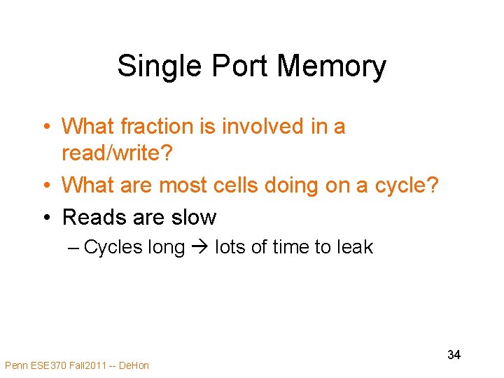
Single Port Memory • What fraction is involved in a read/write? • What are most cells doing on a cycle? • Reads are slow – Cycles long lots of time to leak Penn ESE 370 Fall 2011 -- De. Hon 34
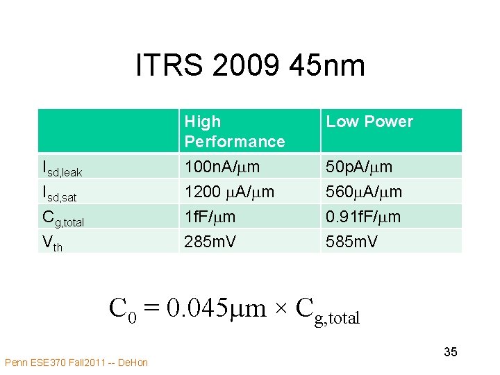
ITRS 2009 45 nm Isd, leak Isd, sat Cg, total Vth High Performance Low Power 100 n. A/mm 1200 m. A/mm 1 f. F/mm 285 m. V 50 p. A/mm 560 m. A/mm 0. 91 f. F/mm 585 m. V C 0 = 0. 045 mm × Cg, total Penn ESE 370 Fall 2011 -- De. Hon 35
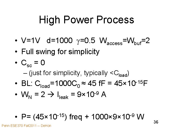
High Power Process • V=1 V d=1000 g=0. 5 Waccess=Wbuf=2 • Full swing for simplicity • Csc = 0 – (just for simplicity, typically <Cload) • BL: Cload=1000 C 0 ≈ 45 f. F = 45× 10 -15 F • WN = 2 Ileak = 9× 10 -9 A • P= (45× 10 -15) freq + 1000× 9× 10 -9 W Penn ESE 370 Fall 2011 -- De. Hon 36
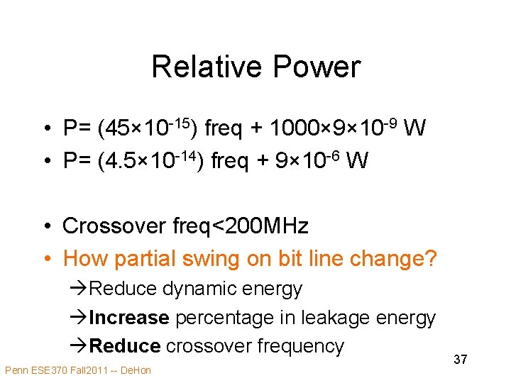
Relative Power • P= (45× 10 -15) freq + 1000× 9× 10 -9 W • P= (4. 5× 10 -14) freq + 9× 10 -6 W • Crossover freq<200 MHz • How partial swing on bit line change? Reduce dynamic energy Increase percentage in leakage energy Reduce crossover frequency Penn ESE 370 Fall 2011 -- De. Hon 37
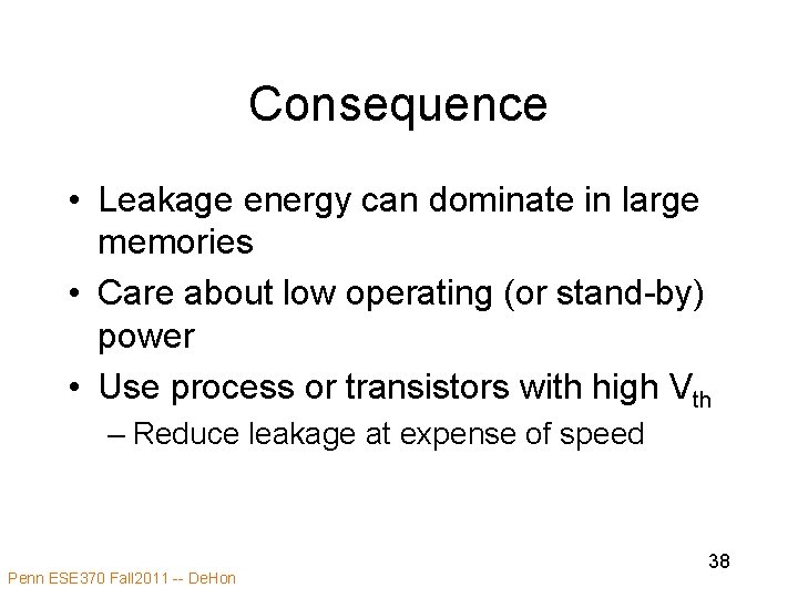
Consequence • Leakage energy can dominate in large memories • Care about low operating (or stand-by) power • Use process or transistors with high Vth – Reduce leakage at expense of speed Penn ESE 370 Fall 2011 -- De. Hon 38
Multiport RAM Skip to admin Penn ESE 370 Fall 2011 -- De. Hon 39
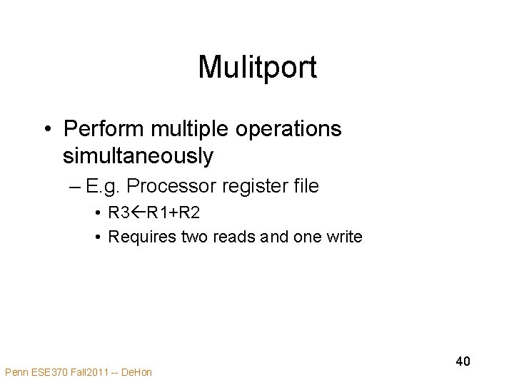
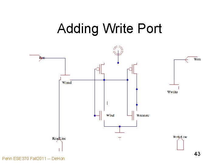
Mulitport • Perform multiple operations simultaneously – E. g. Processor register file • R 3 R 1+R 2 • Requires two reads and one write Penn ESE 370 Fall 2011 -- De. Hon 40
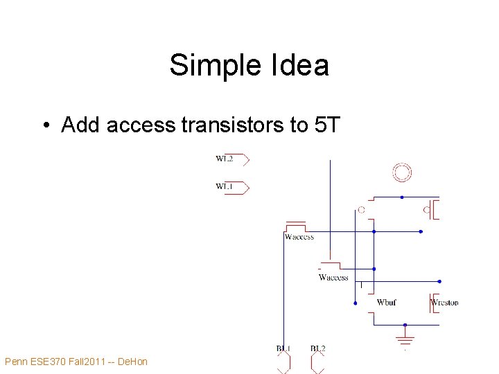
Simple Idea • Add access transistors to 5 T Penn ESE 370 Fall 2011 -- De. Hon 41
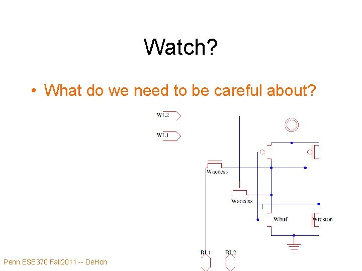
Watch? • What do we need to be careful about? Penn ESE 370 Fall 2011 -- De. Hon 42
Adding Write Port Penn ESE 370 Fall 2011 -- De. Hon 43
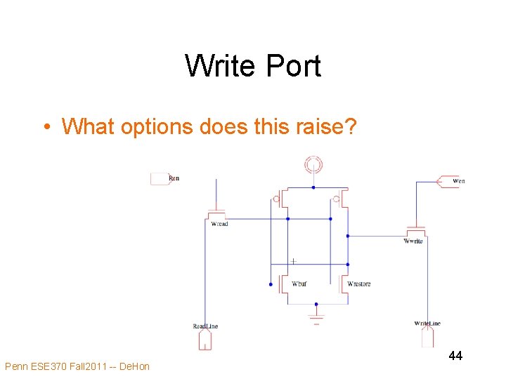
Write Port • What options does this raise? Penn ESE 370 Fall 2011 -- De. Hon 44
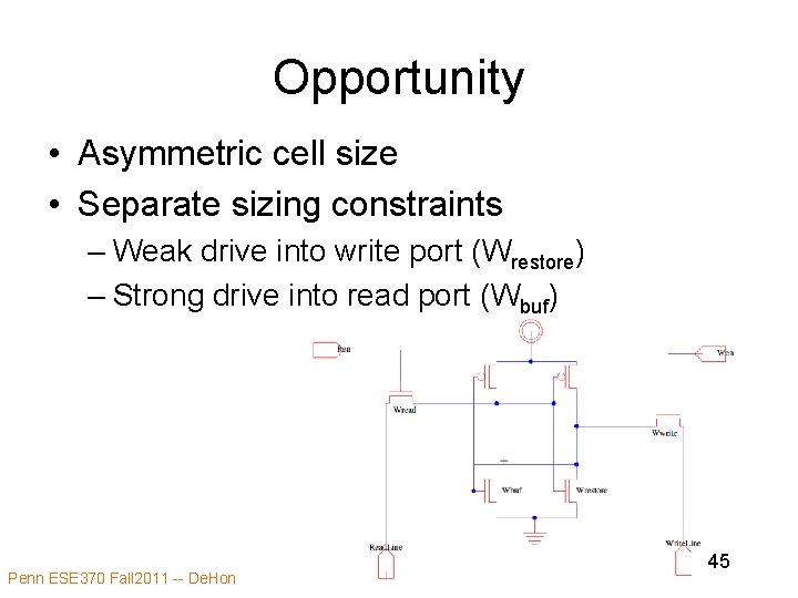
Opportunity • Asymmetric cell size • Separate sizing constraints – Weak drive into write port (Wrestore) – Strong drive into read port (Wbuf) Penn ESE 370 Fall 2011 -- De. Hon 45
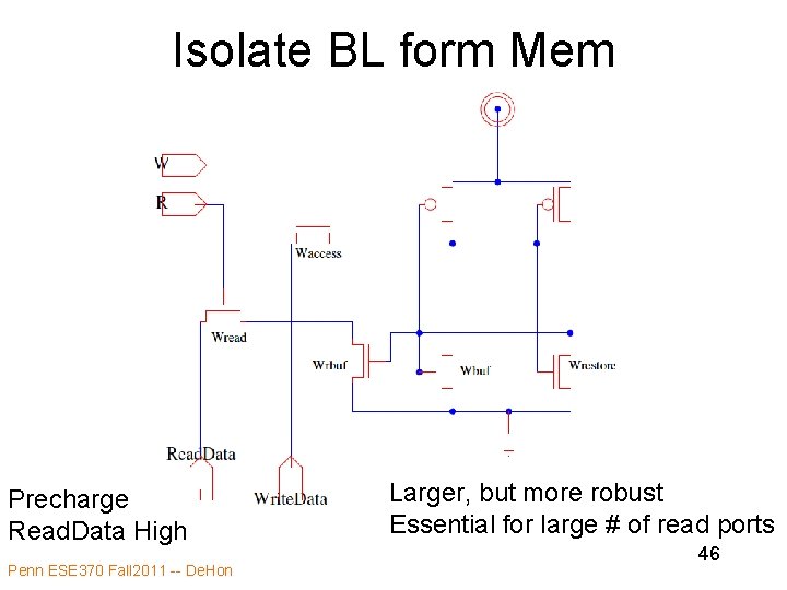
Isolate BL form Mem Precharge Read. Data High Penn ESE 370 Fall 2011 -- De. Hon Larger, but more robust Essential for large # of read ports 46
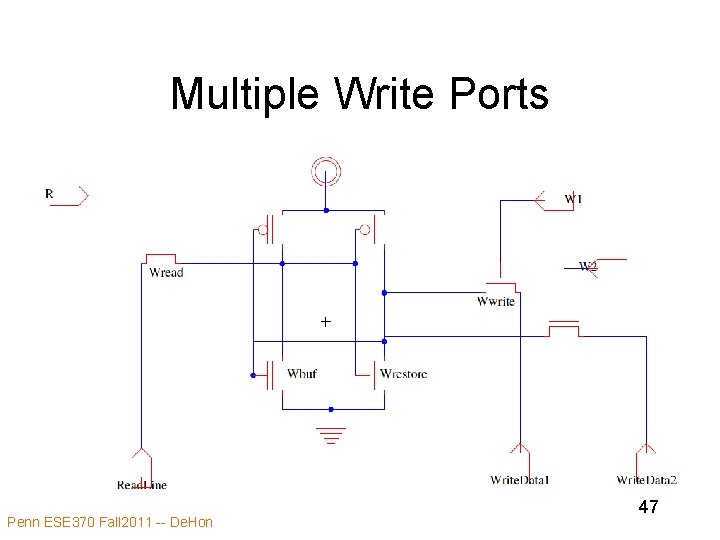
Multiple Write Ports Penn ESE 370 Fall 2011 -- De. Hon 47
Admin • Get started on Project 2 – Timing constraints for correct operation – Select and size your memory cell • Tuesday -- André away—no office hours • Lectures Wednesday and Friday as usual – Finish up memories on Wednesday Penn ESE 370 Fall 2011 -- De. Hon 48
Idea • Memory can be compact • Rich design space • Demands careful sizing Penn ESE 370 Fall 2011 -- De. Hon 49