ESD Basics BASIC CONCEPTS IN ELECTROSTATIC DISCHARGE ESD

ESD Basics BASIC CONCEPTS IN ELECTROSTATIC DISCHARGE (ESD) ©Copyright 2012 DESCO INDUSTRIES INC. Desco. Asia. com
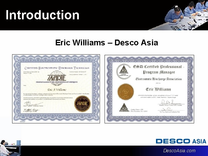
Introduction Eric Williams – Desco Asia Desco. Asia. com

Introduction DESCO INDUSTRIES INC. Desco. Asia. com
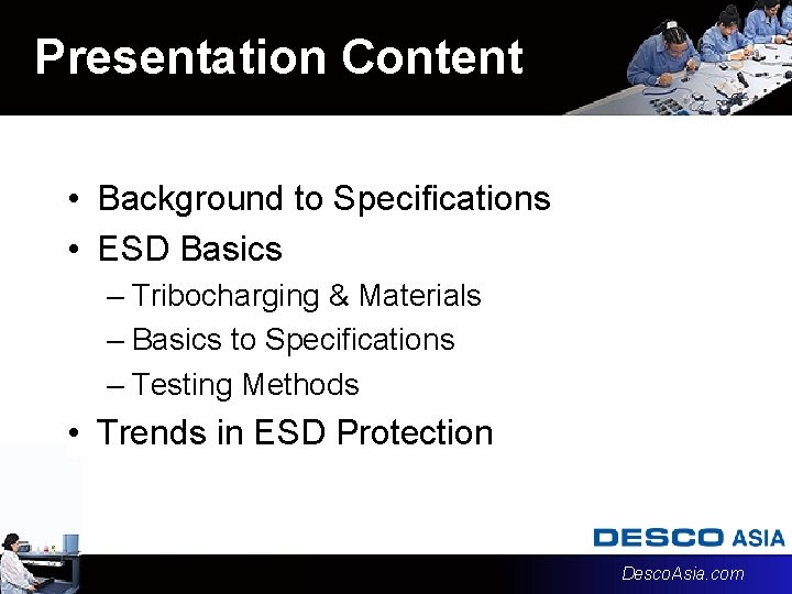
Presentation Content • Background to Specifications • ESD Basics – Tribocharging & Materials – Basics to Specifications – Testing Methods • Trends in ESD Protection Desco. Asia. com
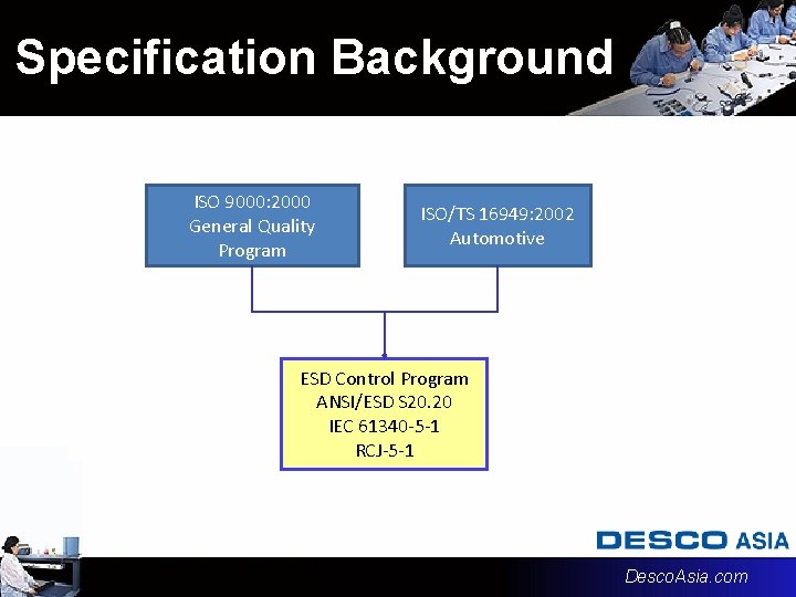
Specification Background ISO 9000: 2000 General Quality Program ISO/TS 16949: 2002 Automotive ESD Control Program ANSI/ESD S 20. 20 IEC 61340 -5 -1 RCJ-5 -1 Desco. Asia. com
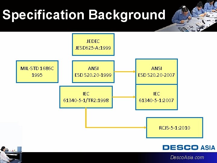
Specification Background JEDEC JESD 625 -A: 1999 MIL-STD 1686 C 1995 ANSI ESD S 20. 20 -1999 IEC 61340 -5 -1/TR 2: 1998 ANSI ESD S 20. 20 -2007 IEC 61340 -5 -1: 2007 RCJS-5 -1: 2010 Desco. Asia. com
ANSI/ESD S 20. 20 -2007 IEC 61340 -5 -1: 2007 Content 6. 0 & 5. 1 ESD Control Program • 6. 1 & 5. 1. 1 ESD Control Plan Requirements • 6. 2 & 5. 1. 2 ESD Control Program Manager or Coordinator • 6. 3 & 5. 1. 3 Tailoring. 7. 0 & 5. 2 ESD Control Program Admin. Requirements • 7. 1 & 5. 2. 1 ESD Control Program Plan • 7. 2 & 5. 2. 2 Training Plan • 7. 3 & 5. 2. 3 Compliance Verification Plan Desco. Asia. com
ANSI/ESD S 20. 20 -2007 IEC 61340 -5 -1: 2007 Content 8. 0 & 5. 3 ESD Control Program Technical Requirements • 8. 1 & 5. 3. 1 Grounding/Equipotential Bonding Systems • 8. 2 & 5. 3. 2 Personnel Grounding • 8. 3 & 5. 3. 3 ESD Protected Areas (EPAs) • 8. 4 & 5. 3. 4 Packaging • 8. 5 & 5. 3. 5 Marking Desco. Asia. com
ESD Basics ESD Control Training Desco. Asia. com
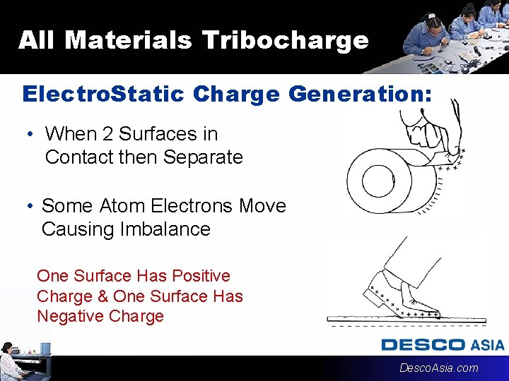
All Materials Tribocharge Electro. Static Charge Generation: • When 2 Surfaces in Contact then Separate • Some Atom Electrons Move Causing Imbalance One Surface Has Positive Charge & One Surface Has Negative Charge Desco. Asia. com
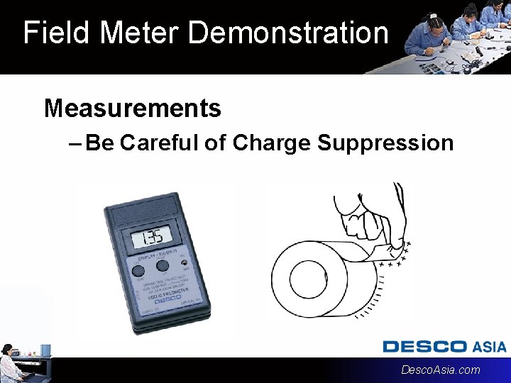
Field Meter Demonstration Measurements – Be Careful of Charge Suppression Desco. Asia. com
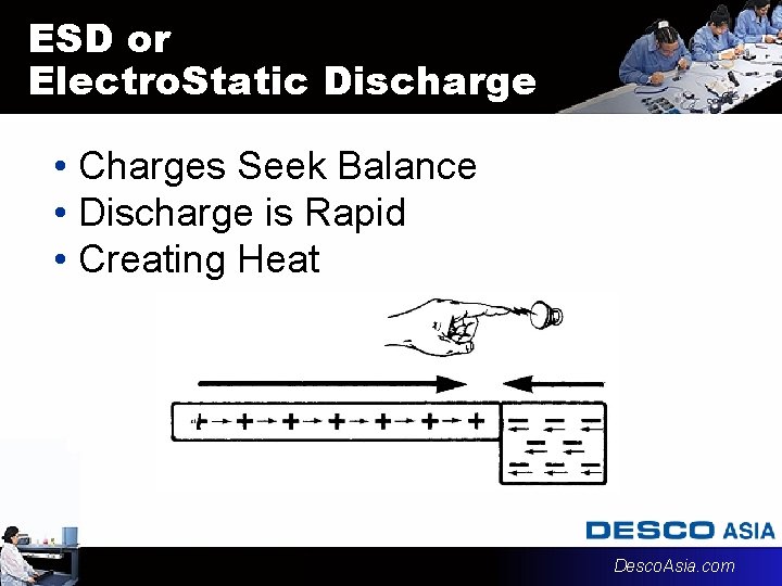
ESD or Electro. Static Discharge • Charges Seek Balance • Discharge is Rapid • Creating Heat Desco. Asia. com
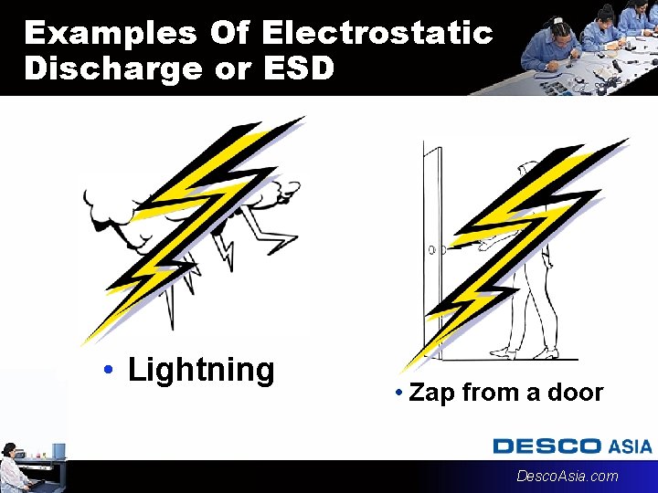
Examples Of Electrostatic Discharge or ESD • Lightning • Zap from a door Desco. Asia. com
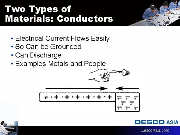
Two Types of Materials: Conductors • Electrical Current Flows Easily • So Can be Grounded • Can Discharge • Examples Metals and People Desco. Asia. com

Two Types of Materials: Insulators • Electrical Current Does Not Flow Easily • So Cannot be Grounded • Example: Plastics • Typically very high charging Desco. Asia. com
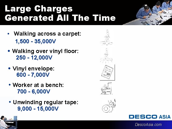
Large Charges Generated All The Time • Walking across a carpet: 1, 500 - 35, 000 V • Walking over vinyl floor: 250 - 12, 000 V • Vinyl envelope: 600 - 7, 000 V • Worker at a bench: 700 - 6, 000 V • Unwinding regular tape: 9, 000 - 15, 000 V Desco. Asia. com
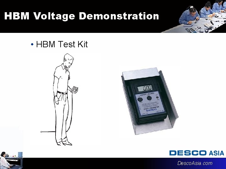
HBM Voltage Demonstration • HBM Test Kit Desco. Asia. com
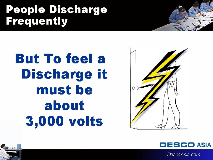
People Discharge Frequently But To feel a Discharge it must be about 3, 000 volts Desco. Asia. com
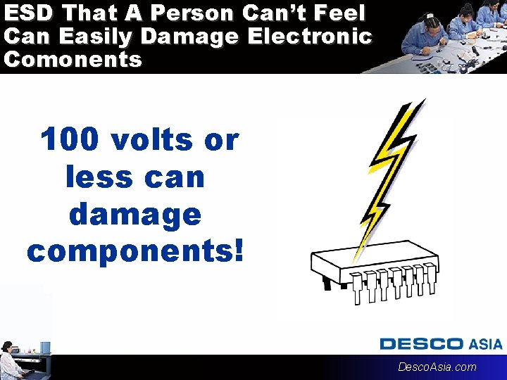
ESD That A Person Can’t Feel Can Easily Damage Electronic Comonents 100 volts or less can damage components! Desco. Asia. com
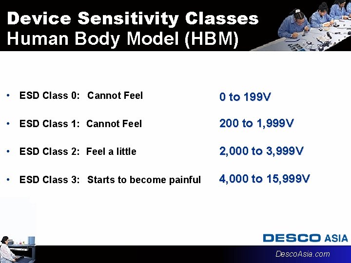
Device Sensitivity Classes Human Body Model (HBM) • ESD Class 0: Cannot Feel 0 to 199 V • ESD Class 1: Cannot Feel 200 to 1, 999 V • ESD Class 2: Feel a little 2, 000 to 3, 999 V • ESD Class 3: Starts to become painful 4, 000 to 15, 999 V Desco. Asia. com
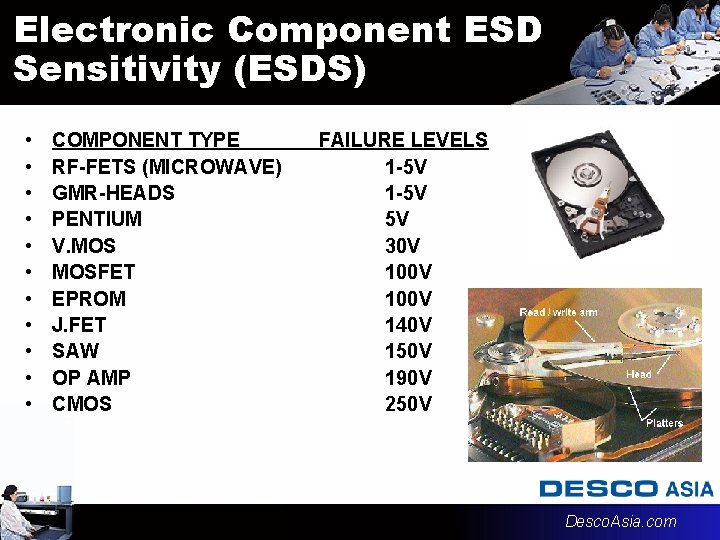
Electronic Component ESD Sensitivity (ESDS) • • • COMPONENT TYPE RF-FETS (MICROWAVE) GMR-HEADS PENTIUM V. MOSFET EPROM J. FET SAW OP AMP CMOS FAILURE LEVELS 1 -5 V 5 V 30 V 100 V 140 V 150 V 190 V 250 V Desco. Asia. com
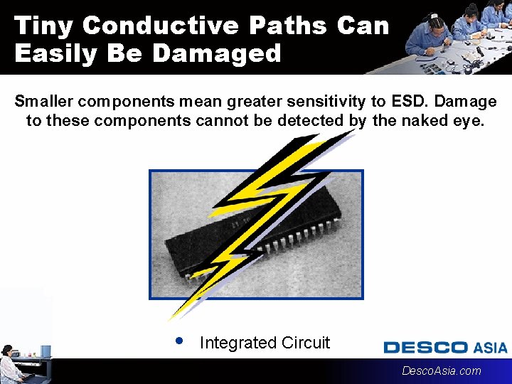
Tiny Conductive Paths Can Easily Be Damaged Smaller components mean greater sensitivity to ESD. Damage to these components cannot be detected by the naked eye. • Integrated Circuit Desco. Asia. com
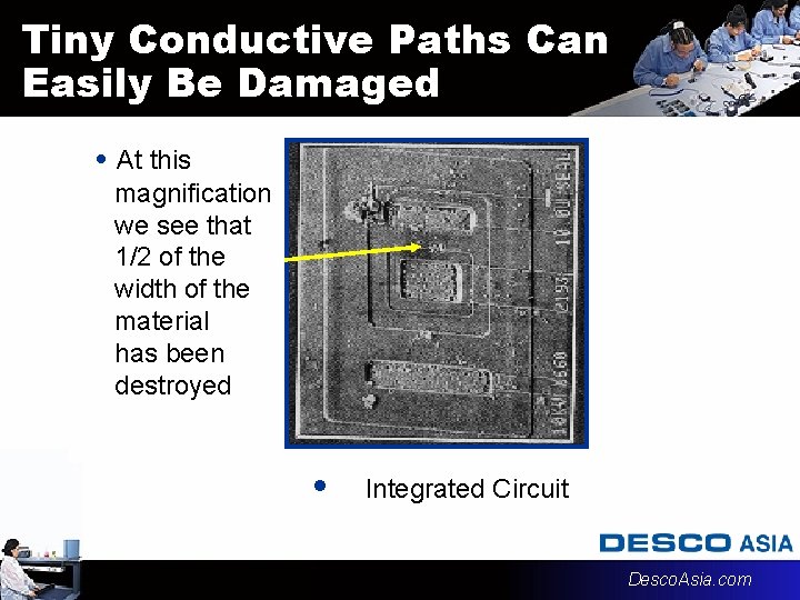
Tiny Conductive Paths Can Easily Be Damaged • At this magnification we see that 1/2 of the width of the material has been destroyed • Integrated Circuit Desco. Asia. com
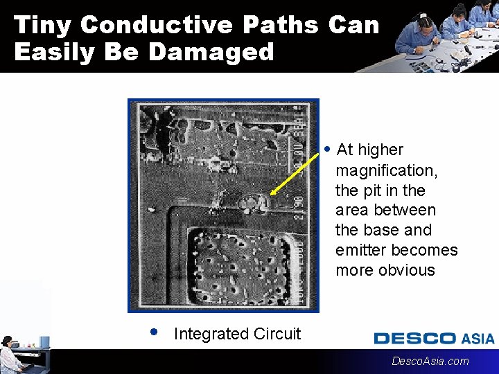
Tiny Conductive Paths Can Easily Be Damaged • At higher magnification, the pit in the area between the base and emitter becomes more obvious • Integrated Circuit Desco. Asia. com
High Magnification Photos of ESD Damage Images of Human Body Model (HBM) ESD damage. Damage visible using Scanning electron micrograph (SEM) after significant enhancement by delayering and etch enhancement. Used with permission of Hi-Rel Laboratories, Inc. Spokane WA 99217 www. hrlabs. com Desco. Asia. com
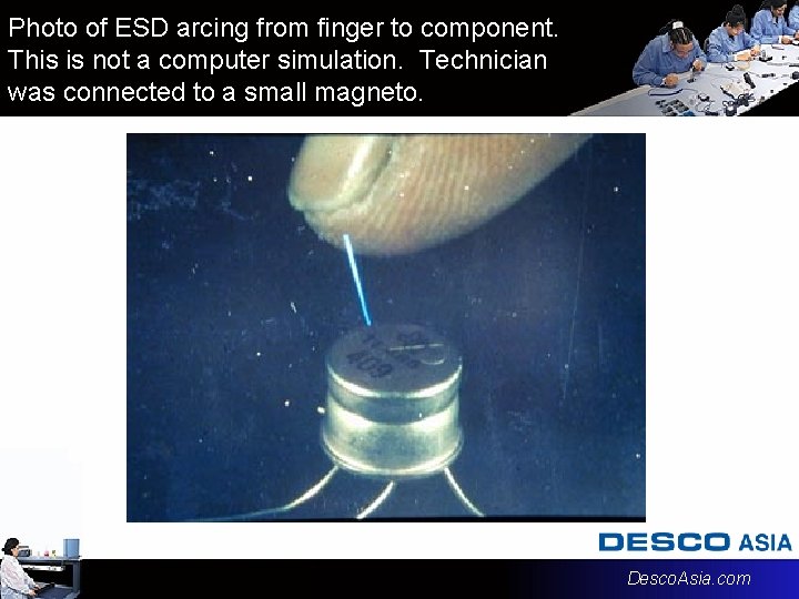
Photo of ESD arcing from finger to component. This is not a computer simulation. Technician was connected to a small magneto. Desco. Asia. com
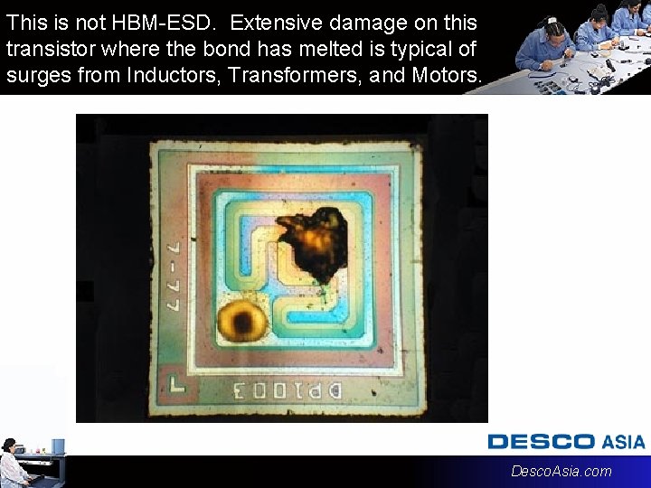
This is not HBM-ESD. Extensive damage on this transistor where the bond has melted is typical of surges from Inductors, Transformers, and Motors. Desco. Asia. com
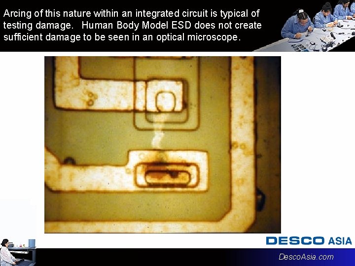
Arcing of this nature within an integrated circuit is typical of testing damage. Human Body Model ESD does not create sufficient damage to be seen in an optical microscope. Desco. Asia. com
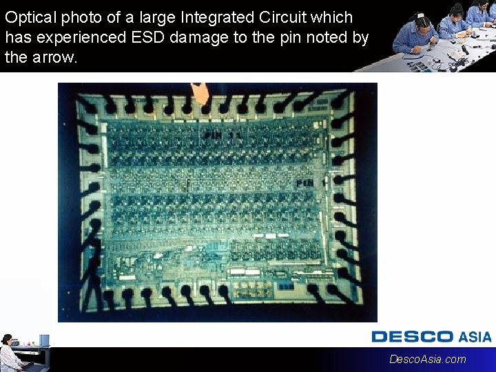
Optical photo of a large Integrated Circuit which has experienced ESD damage to the pin noted by the arrow. Desco. Asia. com
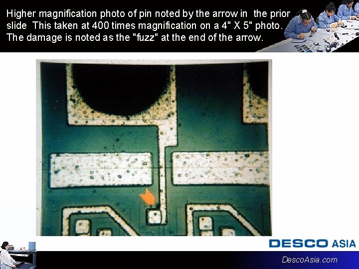
Higher magnification photo of pin noted by the arrow in the prior slide This taken at 400 times magnification on a 4" X 5" photo. The damage is noted as the "fuzz" at the end of the arrow. Desco. Asia. com
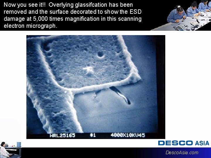
Now you see it!! Overlying glassifcation has been removed and the surface decorated to show the ESD damage at 5, 000 times magnification in this scanning electron micrograph. Desco. Asia. com
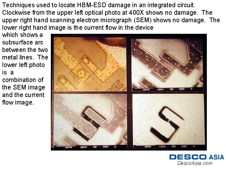
Techniques used to locate HBM-ESD damage in an integrated circuit. Clockwise from the upper left optical photo at 400 X shows no damage. The upper right hand scanning electron micrograph (SEM) shows no damage. The lower right hand image is the current flow in the device which shows a subsurface arc between the two metal lines. The lower left photo is a combination of the SEM image and the current flow image. Desco. Asia. com
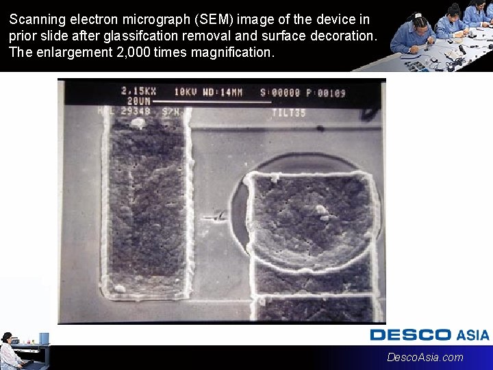
Scanning electron micrograph (SEM) image of the device in prior slide after glassifcation removal and surface decoration. The enlargement 2, 000 times magnification. Desco. Asia. com
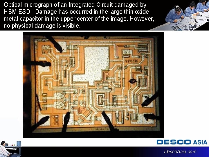
Optical micrograph of an Integrated Circuit damaged by HBM ESD. Damage has occurred in the large thin oxide metal capacitor in the upper center of the image. However, no physical damage is visible. Desco. Asia. com
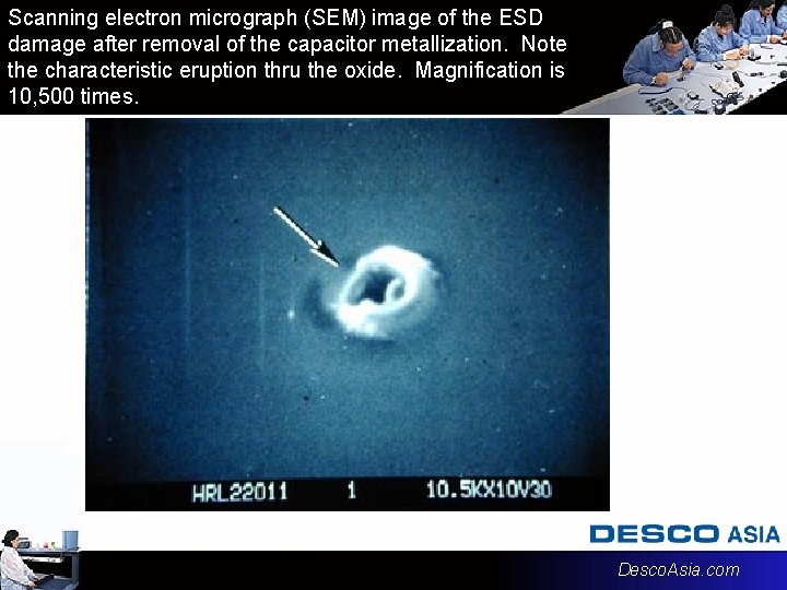
Scanning electron micrograph (SEM) image of the ESD damage after removal of the capacitor metallization. Note the characteristic eruption thru the oxide. Magnification is 10, 500 times. Desco. Asia. com
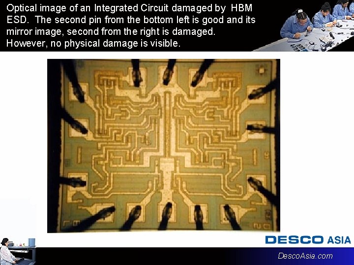
Optical image of an Integrated Circuit damaged by HBM ESD. The second pin from the bottom left is good and its mirror image, second from the right is damaged. However, no physical damage is visible. Desco. Asia. com
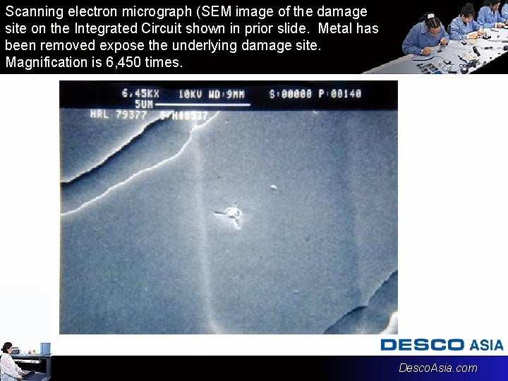
Scanning electron micrograph (SEM image of the damage site on the Integrated Circuit shown in prior slide. Metal has been removed expose the underlying damage site. Magnification is 6, 450 times. Desco. Asia. com
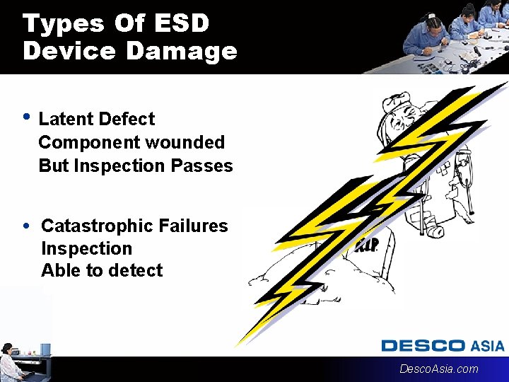
Types Of ESD Device Damage • Latent Defect Component wounded But Inspection Passes • Catastrophic Failures Inspection Able to detect Desco. Asia. com

Latent Defects More Costly • Sub Assembly passes inspection • Product passes inspection • Works a while for customer • Then Upsets & Mysterious Problems • More Returns • More Warranty Costs • Lower Customer Satisfaction Desco. Asia. com

Like Germs, ESD Is The Hidden Enemy Control Germs We are aware of sterilization in medicine Control ESD We should develop the same attitude about ESD Desco. Asia. com
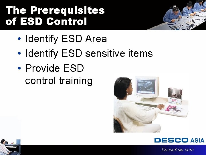
The Prerequisites of ESD Control • Identify ESD Area • Identify ESD sensitive items • Provide ESD control training Desco. Asia. com
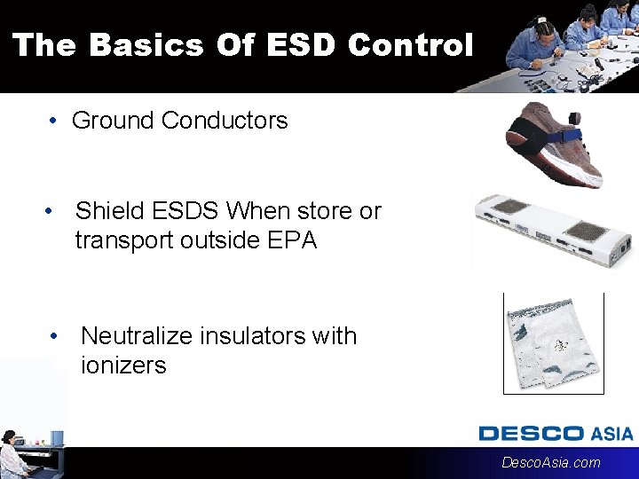
The Basics Of ESD Control • Ground Conductors • Shield ESDS When store or transport outside EPA • Neutralize insulators with ionizers Desco. Asia. com
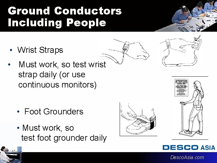
Ground Conductors Including People • Wrist Straps • Must work, so test wrist strap daily (or use continuous monitors) • Foot Grounders • Must work, so test foot grounder daily Desco. Asia. com

When in the EPA, Ground All Conductors Including People • Wrist Strap System Resistance to Ground • Footwear System Resistance to Ground • <3. 5x 10⁷Ω Desco. Asia. com
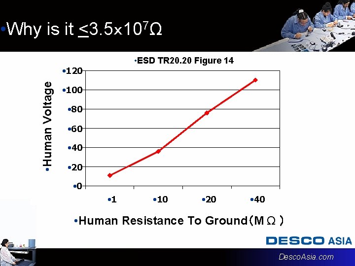
• Why is it <3. 5x 10⁷Ω • ESD TR 20. 20 Figure 14 • Human Voltage • 120 • 100 • 80 • 60 • 40 • 20 • 10 • 20 • 40 • Human Resistance To Ground(M Ω ) Desco. Asia. com
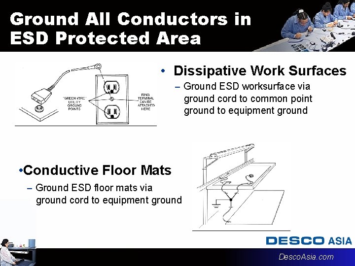
Ground All Conductors in ESD Protected Area • Dissipative Work Surfaces – Ground ESD worksurface via ground cord to common point ground to equipment ground • Conductive Floor Mats – Ground ESD floor mats via ground cord to equipment ground Desco. Asia. com
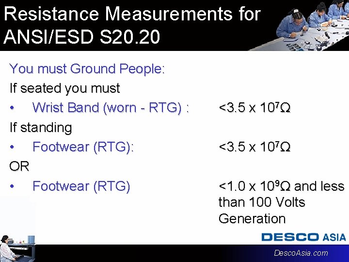
Resistance Measurements for ANSI/ESD S 20. 20 You must Ground People: If seated you must • Wrist Band (worn - RTG) : If standing • Footwear (RTG): OR • Footwear (RTG) <3. 5 x 10⁷Ω <1. 0 x 109Ω and less than 100 Volts Generation Desco. Asia. com
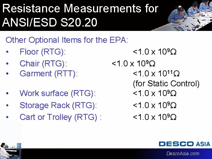
Resistance Measurements for ANSI/ESD S 20. 20 Other Optional Items for the EPA: • Floor (RTG): <1. 0 x 109Ω • Chair (RTG): <1. 0 x 109Ω • Garment (RTT): <1. 0 x 1011Ω (for Static Control) • Work surface (RTG): <1. 0 x 109Ω • Storage Rack (RTG): <1. 0 x 109Ω • Cart or Trolley (RTG) : <1. 0 x 109Ω Desco. Asia. com
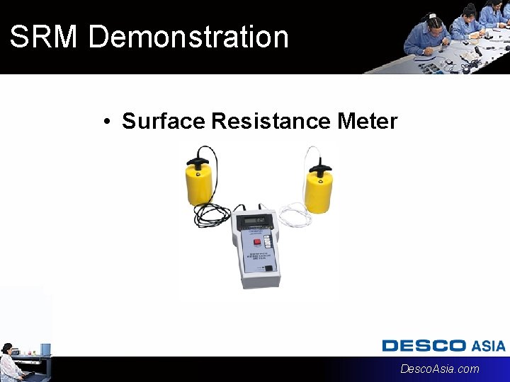
SRM Demonstration • Surface Resistance Meter Desco. Asia. com
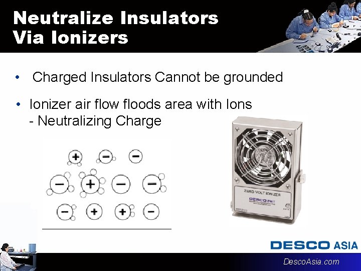
Neutralize Insulators Via Ionizers • Charged Insulators Cannot be grounded • Ionizer air flow floods area with Ions - Neutralizing Charge Desco. Asia. com
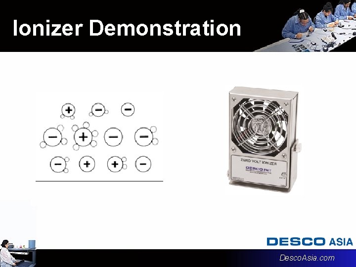
Ionizer Demonstration Desco. Asia. com
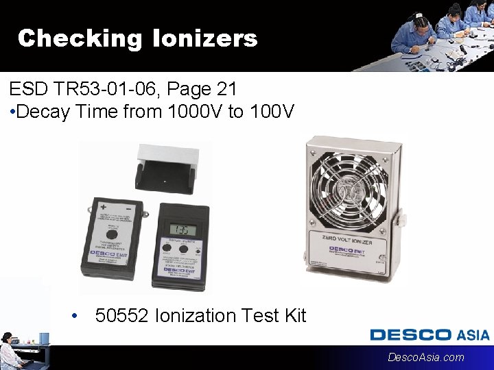
Checking Ionizers ESD TR 53 -01 -06, Page 21 • Decay Time from 1000 V to 100 V • 50552 Ionization Test Kit Desco. Asia. com
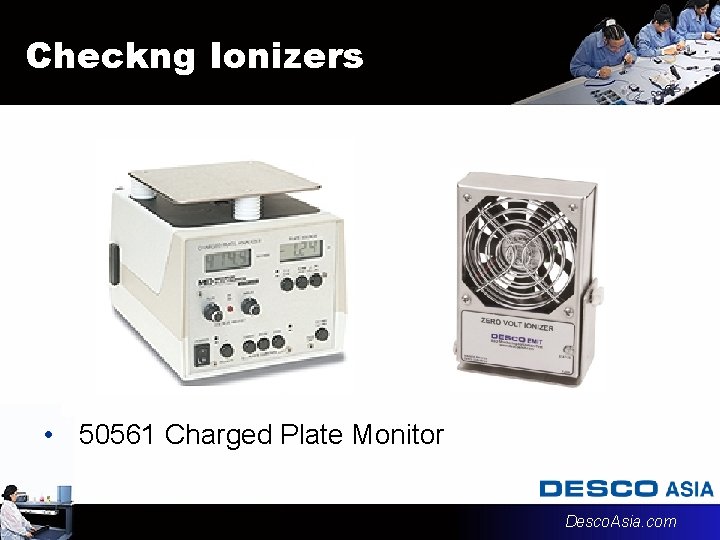
Checkng Ionizers • 50561 Charged Plate Monitor Desco. Asia. com
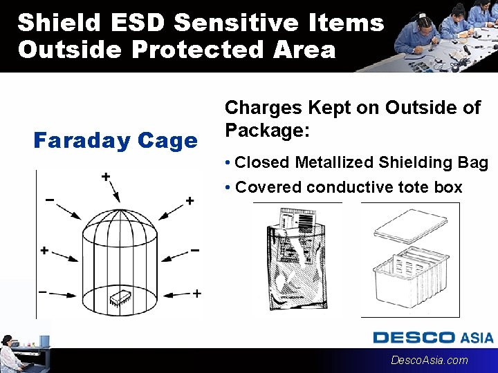
Shield ESD Sensitive Items Outside Protected Area Faraday Cage Charges Kept on Outside of Package: • Closed Metallized Shielding Bag • Covered conductive tote box Desco. Asia. com
Recent Trends in ESD • Focus on different models – Focus on the prevention of static generation and discharge • Difference between models • New Tools for Measurement Desco. Asia. com
Recent Trends 1. Machine Model General Solution - Grounding Machine and Material: Check Ground to Surface Resistance, Ionization, Machine Parts/Component Voltage Measurement. 2. Human Body Model General Solution - Grounding Human Body: ESD Safe Floor, ESD Safe Garment, Wrist Strap, Human Body Voltage Measurement. 3. Charge Device Model General Solution - Control Device Charge: ESD Safe Palette, Ionization, Device Charge Voltage Measurement. 4. Next Control Item: EMI/EMC Control Desco. Asia. com
What is the difference 100 V CDM more Damaging than 100 V HBM? • Q=CV • Coulomb Value 1. Human Body: 100 p. F (10 n. Q) 2. Charge Device: 1 p. F (0. 1 n. Q) *LCD Substrate: 200 to 300 p. F (20 to 30 n. Q) • Size of object 1. HBM(Human Body: 1. 5 to 2 m) 2. CDM(Device: few mm to 1 cm) * LCD Substrate: 2 m X 3 m (max) Desco. Asia. com
What is the difference 100 V CDM more Damaging than 100 V HBM? • Discharging Current 1. 100 VHBM(0. 06 A) 2. 100 VCDM(0. 90 A) * LCD (more than 10 A? ) • Discharge Time 1. HBM(500 n sec) 2. CDM( 1. 5 n sec) * LCD (same as CDM) Desco. Asia. com
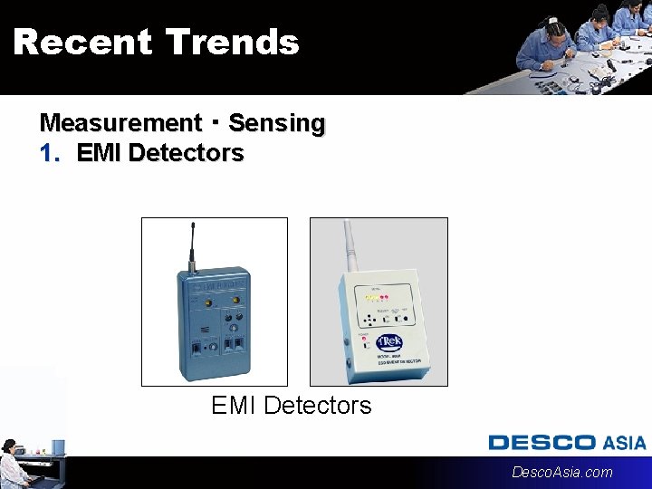
Recent Trends Measurement・Sensing 1. EMI Detectors Desco. Asia. com
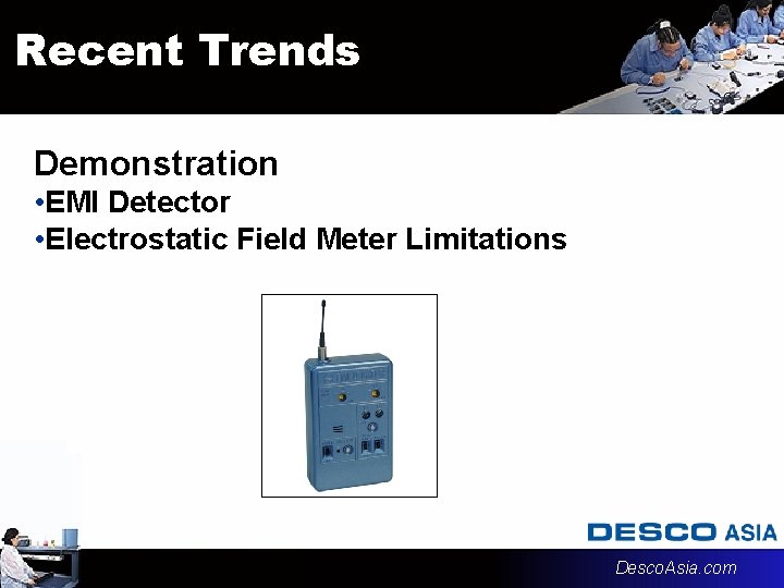
Recent Trends Demonstration • EMI Detector • Electrostatic Field Meter Limitations Desco. Asia. com

ESD Basice Thank you – �� ©Copyright 2012 DESCO INDUSTRIES INC. Desco. Asia. com
- Slides: 61