Epitaxy growth of thin crystalline layers upon a
- Slides: 18

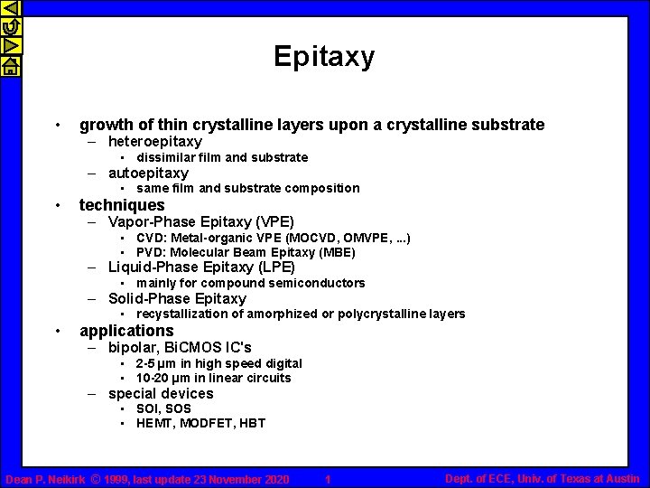
Epitaxy • growth of thin crystalline layers upon a crystalline substrate – heteroepitaxy • dissimilar film and substrate – autoepitaxy • • same film and substrate composition techniques – Vapor-Phase Epitaxy (VPE) • CVD: Metal-organic VPE (MOCVD, OMVPE, . . . ) • PVD: Molecular Beam Epitaxy (MBE) – Liquid-Phase Epitaxy (LPE) • mainly for compound semiconductors – Solid-Phase Epitaxy • • recystallization of amorphized or polycrystalline layers applications – bipolar, Bi. CMOS IC's • 2 -5 µm in high speed digital • 10 -20 µm in linear circuits – special devices • SOI, SOS • HEMT, MODFET, HBT Dean P. Neikirk © 1999, last update 23 November 2020 1 Dept. of ECE, Univ. of Texas at Austin

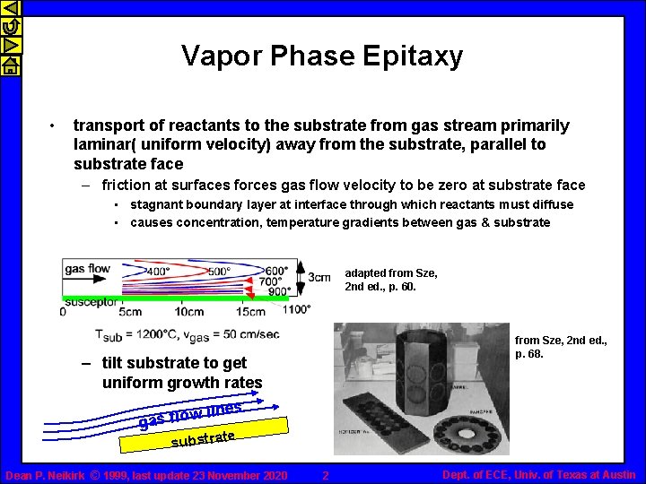
Vapor Phase Epitaxy • transport of reactants to the substrate from gas stream primarily laminar( uniform velocity) away from the substrate, parallel to substrate face – friction at surfaces forces gas flow velocity to be zero at substrate face • stagnant boundary layer at interface through which reactants must diffuse • causes concentration, temperature gradients between gas & substrate adapted from Sze, 2 nd ed. , p. 60. from Sze, 2 nd ed. , p. 68. – tilt substrate to get uniform growth rates ines wl gas flo substrate Dean P. Neikirk © 1999, last update 23 November 2020 2 Dept. of ECE, Univ. of Texas at Austin

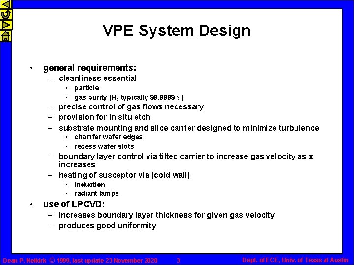
VPE System Design • general requirements: – cleanliness essential • particle • gas purity (H 2 typically 99. 9999%) – precise control of gas flows necessary – provision for in situ etch – substrate mounting and slice carrier designed to minimize turbulence • chamfer wafer edges • recess wafer slots – boundary layer control via tilted carrier to increase gas velocity as x increases – heating of susceptor via (cold wall) • induction • radiant lamps • use of LPCVD: – increases boundary layer thickness for given gas velocity – produces good uniformity Dean P. Neikirk © 1999, last update 23 November 2020 3 Dept. of ECE, Univ. of Texas at Austin

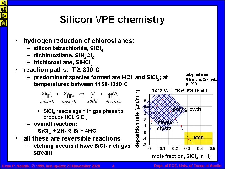
Silicon VPE chemistry • hydrogen reduction of chlorosilanes: – silicon tetrachloride, Si. Cl 4 – dichlorosilane, Si. H 2 Cl 2 – trichlorosilane, Si. HCl 3 • reaction paths: T ≥ 800˚C adapted from Ghandhi, 2 nd ed. , p. 298. • Si. Cl 4 reacts again in gas phase to produce HCl, Si. Cl 2 – overall reaction: Si. Cl 4 + 2 H 2 D Si + 4 HCl • all these are reversible reactions – etching occurs if have Si. Cl 4 rich gas stream Dean P. Neikirk © 1999, last update 23 November 2020 4 deposition rate (mm/min) – predominant species formed are HCl and Si. Cl 2; at temperatures between 1150 -1250˚C 1270°C, H 2 flow rate 1 l/min poly growth single crystal etch mole fraction, Si. Cl 4 in H 2 Dept. of ECE, Univ. of Texas at Austin

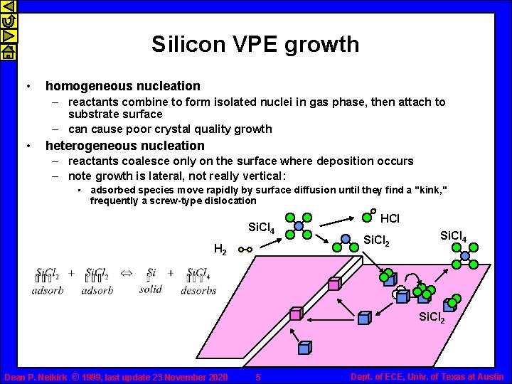
Silicon VPE growth • homogeneous nucleation – reactants combine to form isolated nuclei in gas phase, then attach to substrate surface – can cause poor crystal quality growth • heterogeneous nucleation – reactants coalesce only on the surface where deposition occurs – note growth is lateral, not really vertical: • adsorbed species move rapidly by surface diffusion until they find a "kink, " frequently a screw-type dislocation Si. Cl 4 H 2 HCl Si. Cl 2 Si. Cl 4 Si. Cl 2 Dean P. Neikirk © 1999, last update 23 November 2020 5 Dept. of ECE, Univ. of Texas at Austin

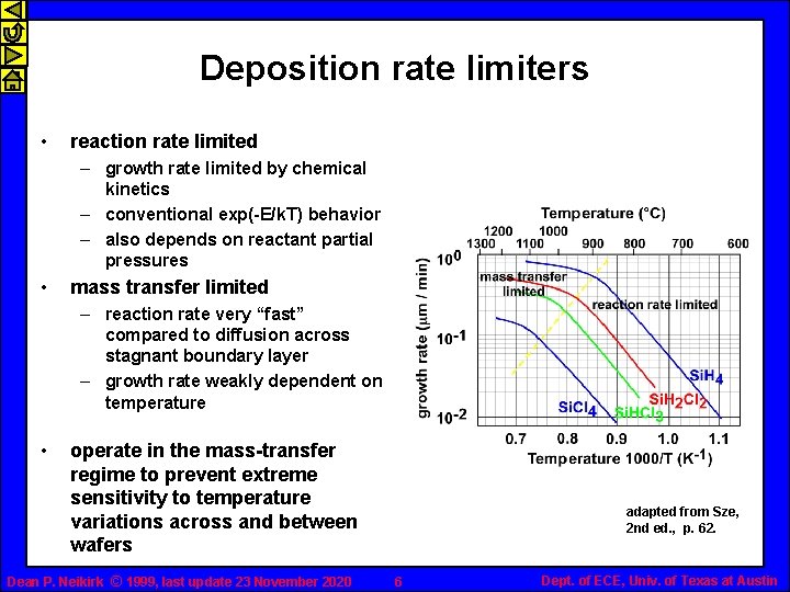
Deposition rate limiters • reaction rate limited – growth rate limited by chemical kinetics – conventional exp(-E/k. T) behavior – also depends on reactant partial pressures • mass transfer limited – reaction rate very “fast” compared to diffusion across stagnant boundary layer – growth rate weakly dependent on temperature • operate in the mass-transfer regime to prevent extreme sensitivity to temperature variations across and between wafers Dean P. Neikirk © 1999, last update 23 November 2020 adapted from Sze, 2 nd ed. , p. 62. 6 Dept. of ECE, Univ. of Texas at Austin

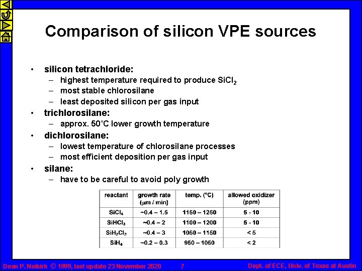
Comparison of silicon VPE sources • silicon tetrachloride: – highest temperature required to produce Si. Cl 2 – most stable chlorosilane – least deposited silicon per gas input • trichlorosilane: – approx. 50˚C lower growth temperature • dichlorosilane: – lowest temperature of chlorosilane processes – most efficient deposition per gas input • silane: – have to be careful to avoid poly growth Dean P. Neikirk © 1999, last update 23 November 2020 7 Dept. of ECE, Univ. of Texas at Austin

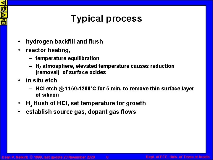
Typical process • hydrogen backfill and flush • reactor heating, – temperature equilibration – H 2 atmosphere, elevated temperature causes reduction (removal) of surface oxides • in situ etch – HCl etch @ 1150 -1200˚C for 5 min. to remove thin surface layer of silicon • H 2 flush of HCl, set temperature for growth • establish source gas, dopant gas flows Dean P. Neikirk © 1999, last update 23 November 2020 8 Dept. of ECE, Univ. of Texas at Austin

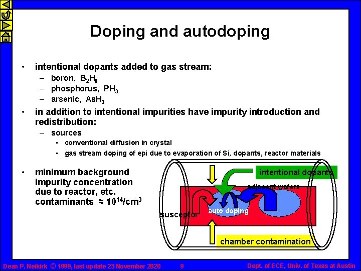
Doping and autodoping • intentional dopants added to gas stream: – boron, B 2 H 6 – phosphorus, PH 3 – arsenic, As. H 3 • in addition to intentional impurities have impurity introduction and redistribution: – sources • conventional diffusion in crystal • gas stream doping of epi due to evaporation of Si, dopants, reactor materials • minimum background impurity concentration due to reactor, etc. contaminants ≈ 1014/cm 3 intentional dopants adjacent wafers susceptor auto doping chamber contamination Dean P. Neikirk © 1999, last update 23 November 2020 9 Dept. of ECE, Univ. of Texas at Austin

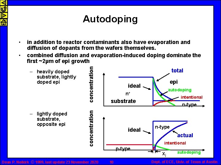
Autodoping – heavily doped substrate, lightly doped epi – lightly doped substrate, opposite epi concentration • in addition to reactor contaminants also have evaporation and diffusion of dopants from the wafers themselves. combined diffusion and evaporation-induced doping dominate the first ~2µm of epi growth total Dean P. Neikirk © 1999, last update 23 November 2020 epi ideal autodoping n+ intentional substrate concentration • ideal n-type actual intentional p-type 10 xj autodoping Dept. of ECE, Univ. of Texas at Austin

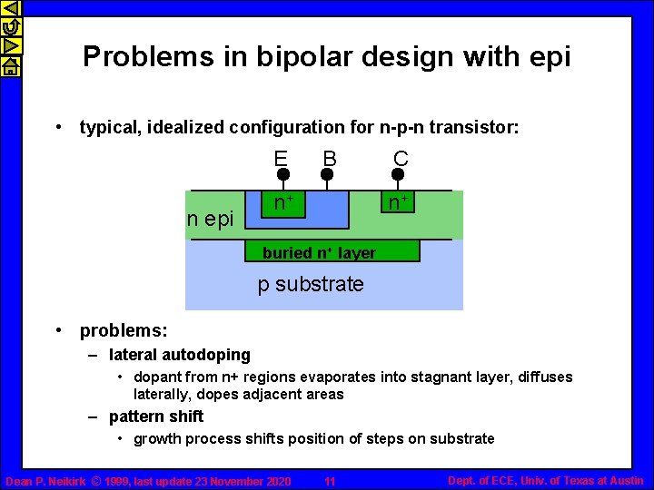
Problems in bipolar design with epi • typical, idealized configuration for n-p-n transistor: E n epi B n+ C n+ buried n+ layer p substrate • problems: – lateral autodoping • dopant from n+ regions evaporates into stagnant layer, diffuses laterally, dopes adjacent areas – pattern shift • growth process shifts position of steps on substrate Dean P. Neikirk © 1999, last update 23 November 2020 11 Dept. of ECE, Univ. of Texas at Austin

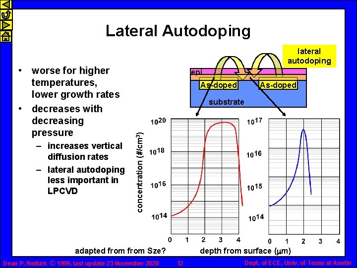
Lateral Autodoping – increases vertical diffusion rates – lateral autodoping less important in LPCVD epi As-doped substrate concentration (#/cm 3) • worse for higher temperatures, lower growth rates • decreases with decreasing pressure lateral autodoping depth from surface (mm) adapted from Sze? Dean P. Neikirk © 1999, last update 23 November 2020 12 Dept. of ECE, Univ. of Texas at Austin

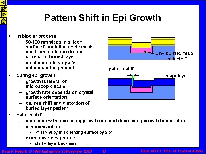
Pattern Shift in Epi Growth • • • in bipolar process: – 50 -100 nm steps in silicon surface from initial oxide mask and from oxidation during drive of n+ buried layer – must maintain steps for subsequent alignment n+ burried “subcollector” pattern shift during epi growth: n epi-layer – growth is lateral on microscopic scale – growth rate depends on crystal surface orientation – causes shift and distortion of buried layer pattern shift: – increases with increasing growth rate and decreasing growth temperature – is minimized for: • <111> Si by misorienting surface by 2 -5˚ – worst case design rule: • shift = layer thickness Dean P. Neikirk © 1999, last update 23 November 2020 13 Dept. of ECE, Univ. of Texas at Austin

Heteroepitaxy • growth of dissimilar film/substrate combination • what do you need? – chemical compatibility – thermal compatibility – “crystal” compatibility • similar lattice structure • similar lattice constants • examples – silicon-on-sapphire • violates lattice match – Alx. Ga 1 -x. As system Dean P. Neikirk © 1999, last update 23 November 2020 14 skip to metals Dept. of ECE, Univ. of Texas at Austin

Silicon on Sapphire • • heteroepitaxial process, usually pyrolisis of silane at 1000˚-1050˚C, ≈ 1 µm thick sapphire chosen for high temperature, chemical stability – – • lattice mismatched at interface aluminum silicate formed at interface aluminum autodoping from substrate thermal expansion coefficient mismatch high defect density: – stacking faults, misfit dislocations – density ≈ inverse with distance to interface – Very short minority-carrier lifetimes • cannot be used for bipolar IC's • used only in MOS devices for – radiation hardness – latch-up immunity Dean P. Neikirk © 1999, last update 23 November 2020 15 Dept. of ECE, Univ. of Texas at Austin

Molecular Beam Epitaxy • non-CVD vapor phase epitaxy via evaporation of material in ultrahigh vacuum environment. By utilizing very low growth rates (≈ 1µm/hour) can tailor doping profiles and composition on a monolayer scale. – – • growth temperatures 400° - 800°C background vacuum pressures ≈ 10 -11 Torr monolayer formation time > 2 days silicon, Si. Ge, Ga. As, Al. Ga. As, II-VI materials all grown machine design: – source materials evaporated from effusion cells • (Si MBE uses e-beam evaporators for Si source) – temperature control critical, up to 1600°C – beams interrupted with mechanical shutters to control composition and doping – all growth chamber surfaces cooled to LN 2 temp to prevent impurity incorporation in films Dean P. Neikirk © 1999, last update 23 November 2020 16 Dept. of ECE, Univ. of Texas at Austin

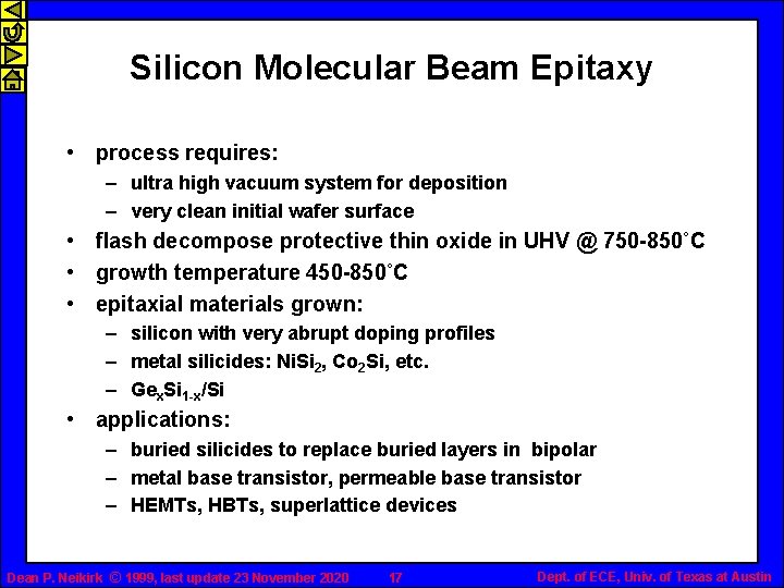
Silicon Molecular Beam Epitaxy • process requires: – ultra high vacuum system for deposition – very clean initial wafer surface • flash decompose protective thin oxide in UHV @ 750 -850˚C • growth temperature 450 -850˚C • epitaxial materials grown: – silicon with very abrupt doping profiles – metal silicides: Ni. Si 2, Co 2 Si, etc. – Gex. Si 1 -x/Si • applications: – buried silicides to replace buried layers in bipolar – metal base transistor, permeable base transistor – HEMTs, HBTs, superlattice devices Dean P. Neikirk © 1999, last update 23 November 2020 17 Dept. of ECE, Univ. of Texas at Austin

Summary Slide • • Epitaxy Silicon VPE growth Doping and autodoping Pattern Shift in Epi Growth Heteroepitaxy Epitaxial Growth of Ga. As next topic: metallization Dean P. Neikirk © 1999, last update 23 November 2020 18 Dept. of ECE, Univ. of Texas at Austin