EPDTDD Detector Development SSD Solid State Detectors SSD
![SSD: Generic R&D Damage: We are loosing the gain! val [SSD: submitted for publication] SSD: Generic R&D Damage: We are loosing the gain! val [SSD: submitted for publication]](https://slidetodoc.com/presentation_image_h2/8eee285bed69468031d46aef4cfd42e0/image-6.jpg)
- Slides: 7

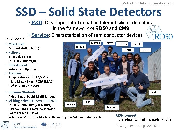
EP-DT-DD – Detector Development SSD – Solid State Detectors SSD Team: • R&D: Development of radiation tolerant silicon detectors in the framework of RD 50 and CMS • Service: Characterization of semiconductor devices • CERN Staff Michael Moll (0. 6 FTE) Matteo Esteban Pedro Marcos Joaquin Sofia • Fellows Laura Julio Calvo Pinto Matteo Centis Vignali • Ph. D student Sofia Otero Ugobono • Trainees Joaquin Gonzalez (SSD/CMS) Isidro Mateu Suau (RD 50/IRRAD) Pedro Almeida (RD 50) • Summer Students Isidro Pablo, Jared, David, Matthias, Ana • Visiting Scientist (>2 m at CERN ): Julio Geetika Marcos Fernandez (Santander) Michael Esteban Curras Rivera (Santander) Laura Franconi (Oslo) RD 50 support: Sebastian White , Geetika Jain (Delhi), Rogelio Palomo Pinto (Sevilla), … Veronique Wedlake, Maurice Glaser EP-DT group meeting 22. 6. 2017

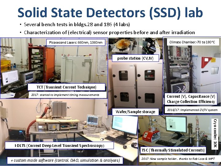
Solid State Detectors (SSD) lab • Several bench tests in bldgs. 28 and 186 (4 labs) • Characterization of (electrical) sensor properties before and after irradiation Climate Chamber: -70 to 180 C Picosecond Lasers: 660 nm, 1060 nm probe station (CV, IV) TCT (Transient Current Technique) 2017: started to implement timing measurements Current (V), Capacitance (V) Charge Collection Efficiency Wafer/Sample storage + custom made software (control, DAQ, simulation & analyses) TSC (Thermally Stimulated Currents) Cryo cooler: 10 K I-DLTS (Current Deep Level Transient Spectroscopy) 2016/17: Implemented CV/IV system 2017: New sample holder…thanks to Rob Loos & MPT EP-DT group meeting 22. 6. 2017 2

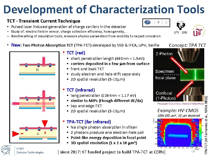
Development of Characterization Tools TCT - Transient Current Technique • Pulsed laser induced generation of charge carriers in the detector – Study of: electric field in sensor, charge collection efficiency, homogeneity, . . – Benchmarking of simulation tools, measure physics parameters from mobility to impact ionization • New: Two Photon Absorption TCT (TPA-TCT) developed by SSD & IFCA, UPV, Seville Concept: TPA TCT • TCT (red) § § § short penetration length (660 nm = 1. 9 e. V) carriers deposited in a few mm from surface front and back TCT study electron and hole drift separately 2 D spatial resolution (5 -10 mm) § § long penetration (1064 nm = 1. 17 e. V) similar to MIPs (though different d. E/dx) top and edge-TCT 2 D spatial resolution (5 -10 mm) Example: HV-CMOS 100 x 100 mm 2, 10 mm depleted • TPA-TCT (far infrared) § § No single photon absorption in silicon 2 photons produce one electron-hole pair Point-like energy deposition in focal point 3 D spatial resolution (1 x 10 mm 3) [ since 2017: KT funded project to build TPA-TCT at CERN] -3 - TPA-TCT [M. Fernandez et al. , NIMA 2016] • TCT (infrared)

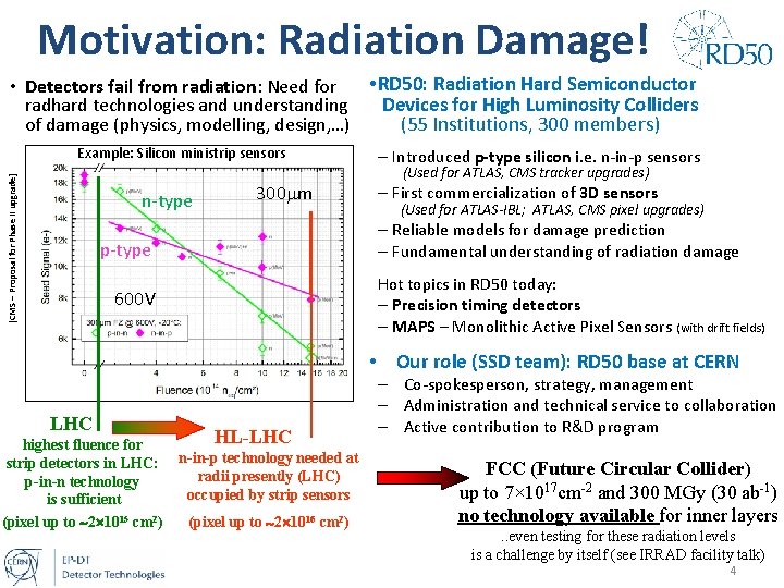
Motivation: Radiation Damage! • RD 50: Radiation Hard Semiconductor • Detectors fail from radiation: Need for Devices for High Luminosity Colliders radhard technologies and understanding of damage (physics, modelling, design, …) (55 Institutions, 300 members) [CMS – Proposal for Phase II upgrade] Example: Silicon ministrip sensors n-type 300 mm – Introduced p-type silicon i. e. n-in-p sensors (Used for ATLAS, CMS tracker upgrades) – First commercialization of 3 D sensors (Used for ATLAS-IBL; ATLAS, CMS pixel upgrades) – Reliable models for damage prediction – Fundamental understanding of radiation damage p-type Hot topics in RD 50 today: – Precision timing detectors – MAPS – Monolithic Active Pixel Sensors (with drift fields) 600 V • Our role (SSD team): RD 50 base at CERN LHC highest fluence for strip detectors in LHC: p-in-n technology is sufficient (pixel up to 2 1015 cm 2) HL-LHC n-in-p technology needed at radii presently (LHC) occupied by strip sensors (pixel up to 2 1016 cm 2) – Co-spokesperson, strategy, management – Administration and technical service to collaboration – Active contribution to R&D program FCC (Future Circular Collider) up to 7× 1017 cm-2 and 300 MGy (30 ab-1) no technology available for inner layers. . even testing for these radiation levels is a challenge by itself (see IRRAD facility talk) 4

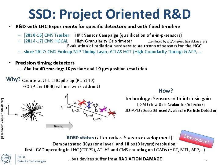
SSD: Project Oriented R&D • R&D with LHC Experiments for specific detectors and with fixed timeline – [2010 -16] CMS Tracker HPK Sensor Campaign (qualification of n-in-p-sensors) – [2014 -17] CMS HGCAL High Granularity Calorimeter …continued by LCD/DT group (Eva Sicking et al. ) Evaluation of radiation hardness to neutrons of sensors for the HGC – since 2017: CMS Endcap MIP Timing Layer, ATLAS HGT (High Granularity Timing) & AFP, … • Precision timing detectors – Aim for 4 D tracking: 10 ps time and 10 mm position resolution Why? Counteract HL-LHC pile-up (PU 140) [H. Sadrozinski ar. Xiv: 1704. 08666] FCC (PU 1000) will not work without! How? Technology: Sensors with intrinsic gain LGAD (Low Gain Avalanche Detectors) DD-APD (Deep Diffused Avalanche Particle Detector) RD 50 status (after only 5 years development) Impr essiv e! Demonstrated 30 ps (one layer) and 18 ps (3 layers) resolution; first LGAD operating in LHC (CTPPS), ATLAS and CMS counting on LGADs (HGT, MTL, AFP, …) …but devices suffer from RADIATION DAMAGE 5
![SSD Generic RD Damage We are loosing the gain val SSD submitted for publication SSD: Generic R&D Damage: We are loosing the gain! val [SSD: submitted for publication]](https://slidetodoc.com/presentation_image_h2/8eee285bed69468031d46aef4cfd42e0/image-6.jpg)
SSD: Generic R&D Damage: We are loosing the gain! val [SSD: submitted for publication] • LGAD Low Gain Avalanche Detector Exa Accep mple: tor rem o A gain layer produced by Boron doping provides a high electric field that leads to charge multiplication (i. e. increased signal improved timing) • Problem: Loss of gain in LGAD sensors due to radiation damage • Reason (most likely, ongoing R&D effort): Boron doping is de-activated by radiation damage After irradiation: Boron bound in defects; visible as defect levels Signal [f. F] [SSD & L. Makarenko (Minsk) ] [B] B i Cs B i Oi Temperature [K] Damage parameterization Silicon with different Boron content (i. e. different resisitivity) 10 Wcm 50 Wcm 250 Wcm Epi-p, 50 mm 1000 Wcm • Mitigation approach (under study) Fluence [neq/cm 2] – Replace Boron by Gallium (another acceptor type) – Enrich silicon with Carbon (acts as defect getter) 6 [SSD: presented on RD 50 Workshop in June 2017] Defect spectroscopy (DLTS) Fluence [neq/cm 2]

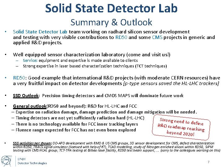
Solid State Detector Lab Summary & Outlook • Solid State Detector Lab team working on radhard silicon sensor development and testing with very visible contributions to RD 50 and some CMS projects in generic and applied R&D projects. • Well equipped sensor characterization laboratory (come and visit us!) – Service: equipment and expertise is made available to clients – Strong expertise in laser based characterization techniques (TCT techniques) • RD 50: Good example that international R&D projects (with moderate CERN resources) have a very fruitful impact on detector developments [p-type sensors saved the HL-LHC trackers] • SSD Outlook: Precision timing detectors and CMOS MAPS will dominate future work • • General outlook(RD 50 and beyond): R&D for HL-LHC and FCC – Expertise on radiation damage, damage prediction and damage mitigation will be needed. – Timing detectors are not yet sufficiently radiation hard (HL-LHC) Strong need to define – There is no technology available for FCC inner tracking layers R&D roadma p reaching – Fluence range expected for FCC has not even been explored beyond 2020 ! SSD activities not shown: DD-APD development with RMD & US CMS groups, 3 D sensor development for CMS, defect characterization within RD 50, TRACS signal simulator (licensed with help of KT), TCAD modelling, study of Nitrogen enriched silicon within RD 50, Si. PM testing with CMS HCAL group; TCT-TPA testing at Bilbao laser facility, RD 50 test beam support, …. (sorry to the colleagues working on this) 7