ENT 162 Analog Electronics Assignment 1 2 Stage
- Slides: 6

ENT 162 Analog Electronics Assignment 1 2 -Stage Amplifier

Overview • Audio preamplifier is to be developed for small PA system. Preamplifier will have microphone input, and its output will drive power amplifier. Power amplifier will drive speaker. DC supply voltages are provided by a battery pack or by electronic power supply. Amplifier should operate from 30 Vdc to get a large enough signal voltage swing to provide 6 W to speaker.

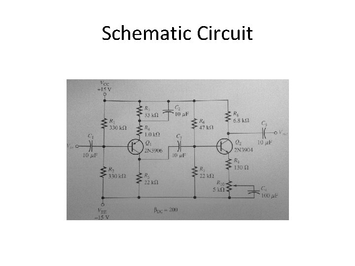
Schematic Circuit

• Input to first stage is from microphone, output of second stage will drive power amplifier. • Because IC regulators are not available above 24 V, dual +/-15 Vdc supplies are used in this system instead of single supply. The operation is essentially the same as if single 30 Vdc source is used. Potentiometer at output provides gains adjustment for volume control. Preamp is to operate with peak input signal range from 25 m. V to 50 m. V. Minimum range of voltage gain adjustment is from 90 to 170. Assume beta ac = beta DC =200

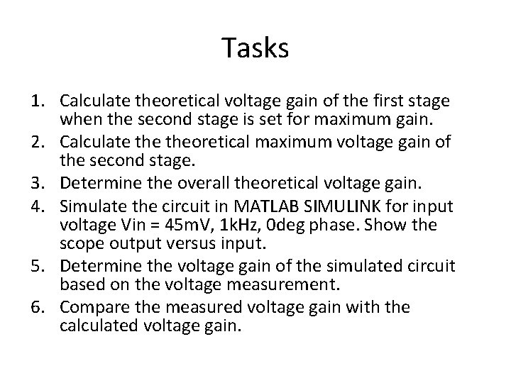
Tasks 1. Calculate theoretical voltage gain of the first stage when the second stage is set for maximum gain. 2. Calculate theoretical maximum voltage gain of the second stage. 3. Determine the overall theoretical voltage gain. 4. Simulate the circuit in MATLAB SIMULINK for input voltage Vin = 45 m. V, 1 k. Hz, 0 deg phase. Show the scope output versus input. 5. Determine the voltage gain of the simulated circuit based on the voltage measurement. 6. Compare the measured voltage gain with the calculated voltage gain.

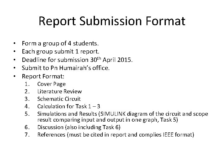
Report Submission Format • • • Form a group of 4 students. Each group submit 1 report. Deadline for submission 30 th April 2015. Submit to Pn Humairah’s office. Report Format: 1. 2. 3. 4. 5. 6. 7. Cover Page Literature Review Schematic Circuit Calculation for Task 1 – 3 Simulations and Results (SIMULINK diagram of the circuit and scope result comparing input and output in one graph, Task 5) Discussion (also including Task 6) References (must be cited in report and complies IEEE format)