ENT 116 DIGITAL ELECTRONIC PRINCIPLES Combinational Logic Circuits
ENT 116 -DIGITAL ELECTRONIC PRINCIPLES Combinational Logic Circuits Part-1 Prepared by Dr M. MURUGAPPAN Bio-Medical Electronics Programme School of Mechatronics Engineering Universiti Malaysia Perlis
Topic Coverage Define, Analyze, and Design Arithmetic logic circuit, logic control, project logic, and time diagram Define, Analyze, and Design the applications of Combinational Logic Circuit design (E. g: Adder, MUX, DEMUX, Decoders, and Encoder)
Part-1 – Design Procedure ◦ Design Steps Specification Formulation Optimization Technology Mapping ◦ Beginning Hierarchical Design ◦ Technology Mapping - AND, OR, and NOT to NAND or NOR ◦ Verification Manual Simulation
Introduction Logic Gates: Electronic components that compute a Boolean function of their inputs. Logic Circuit: A combination of logic gates that computes some Boolean function. ◦ Every circuit can be expressed in three ways: ◦ Schematic Diagram ◦ Logic Expression ◦ Truth Table
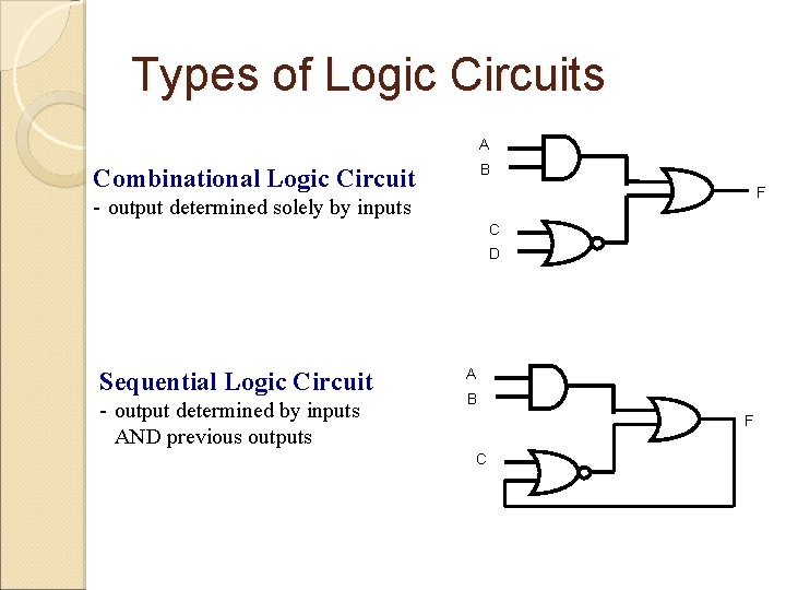
Types of Logic Circuits A B Combinational Logic Circuit F - output determined solely by inputs C D Sequential Logic Circuit - output determined by inputs AND previous outputs A B F C
Part 2 – Combinational Logic ◦ Functions and functional blocks ◦ Rudimentary logic functions ◦ Decoding using Decoders Implementing Combinational Functions with Decoders ◦ Encoding using Encoders ◦ Selecting using Multiplexers Implementing Combinational Functions with Multiplexers
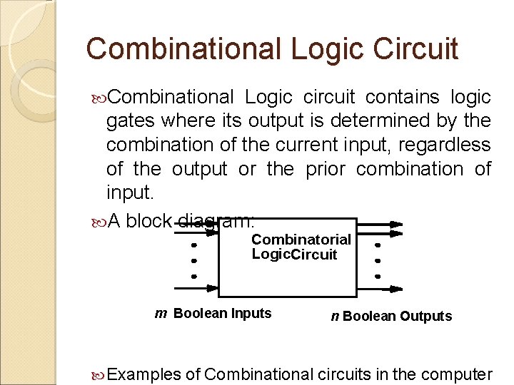
Combinational Logic Circuit Combinational Logic circuit contains logic gates where its output is determined by the combination of the current input, regardless of the output or the prior combination of input. A block diagram: Combinatorial Logic. Circuit m Boolean Inputs n Boolean Outputs Examples of Combinational circuits in the computer
Basic Combinational Logic Circuits AND-OR Logic AND-OR Invert Logic Exclusive OR (EXOR) Logic Exclusive NOR (EXNOR) Logic
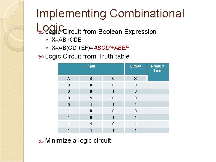
Implementing Combinational Logic Circuit from Boolean Expression ◦ X=AB+CDE ◦ X=AB(CD’+EF)=ABCD’+ABEF Logic Circuit from Truth table Input Output A B C X 0 0 0 1 1 0 0 0 1 1 1 1 0 1 1 1 Minimize a logic circuit Product Term
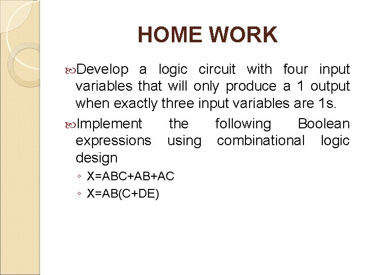
HOME WORK Develop a logic circuit with four input variables that will only produce a 1 output when exactly three input variables are 1 s. Implement the following Boolean expressions using combinational logic design ◦ X=ABC+AB+AC ◦ X=AB(C+DE)
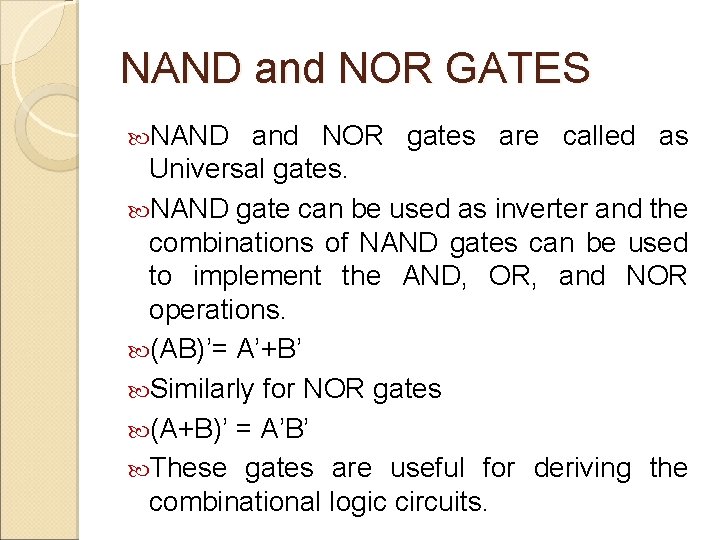
NAND and NOR GATES NAND and NOR gates are called as Universal gates. NAND gate can be used as inverter and the combinations of NAND gates can be used to implement the AND, OR, and NOR operations. (AB)’= A’+B’ Similarly for NOR gates (A+B)’ = A’B’ These gates are useful for deriving the combinational logic circuits.
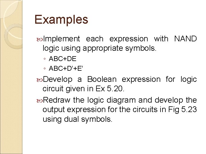
Examples Implement each expression with NAND logic using appropriate symbols. ◦ ABC+DE ◦ ABC+D’+E’ Develop a Boolean expression for logic circuit given in Ex 5. 20. Redraw the logic diagram and develop the output expression for the circuits in Fig 5. 23 using dual symbols.
Combinational Logic Design A process with 5 steps ◦ Specification ◦ Formulation ◦ Optimization ◦ Technology mapping ◦ Verification Examples of functional logic circuits ◦ Decoders ◦ Encoders ◦ Code converters ◦ Multiplexers
Specifications step Write a specification for the circuits Specification includes ◦ What are the inputs: how many, how many bits in a given output, how are they grouped, , are they control, are they active high? ◦ What are the outputs: how many and how many bits in a each, active high, active low, tristate output? ◦ The functional operation that takes place in the chip, i. e. , for given inputs what will appear on the outputs. 14
Formulation step Convert the specifications into a variety forms for optimal implementation. ◦ Possible forms Truth Tables Boolean Expressions K-maps Binary Decision Diagrams IF THE SPECIFCATION IS ERRONOUS OR INCOMPLETE (open for various interpretation) then the circuit will perform as specified but will not perform as desired. 15
Last 3 steps Best illustrated by example ◦ A BCD to Excess-3 code converter 16
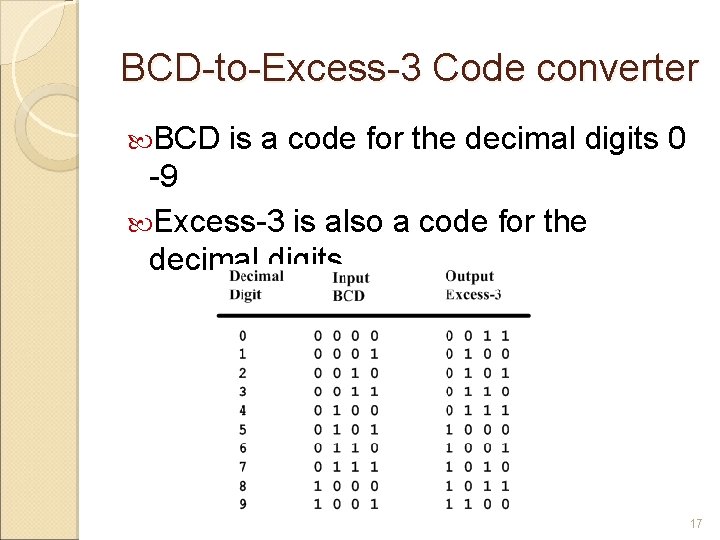
BCD-to-Excess-3 Code converter BCD is a code for the decimal digits 0 -9 Excess-3 is also a code for the decimal digits 17
Specification of BCD-to. Excess 3 Inputs: a BCD input, A, B, C, D with A as the most significant bit and D as the least significant bit. Outputs: an Excess-3 output W, X, Y, Z that corresponds to the BCD input. Internal operation – circuit to do the conversion in combinational logic. 18
Formulation of BCD-to. Excess-3 code is easily formed by adding a binary 3 to the binary or BCD for the digit. There are 16 possible inputs for both BCD and Excess-3. It can be assumed that only valid BCD inputs will appear so the six combinations not used can be treated as don’t cares. 19
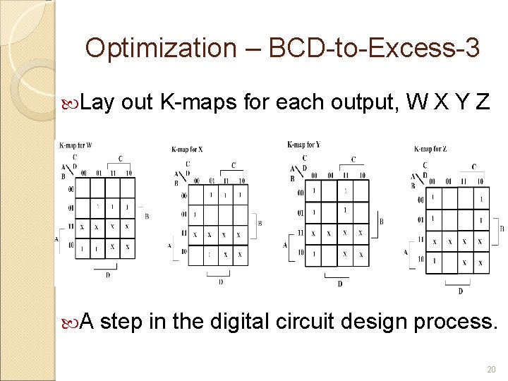
Optimization – BCD-to-Excess-3 Lay A out K-maps for each output, W X Y Z step in the digital circuit design process. 20
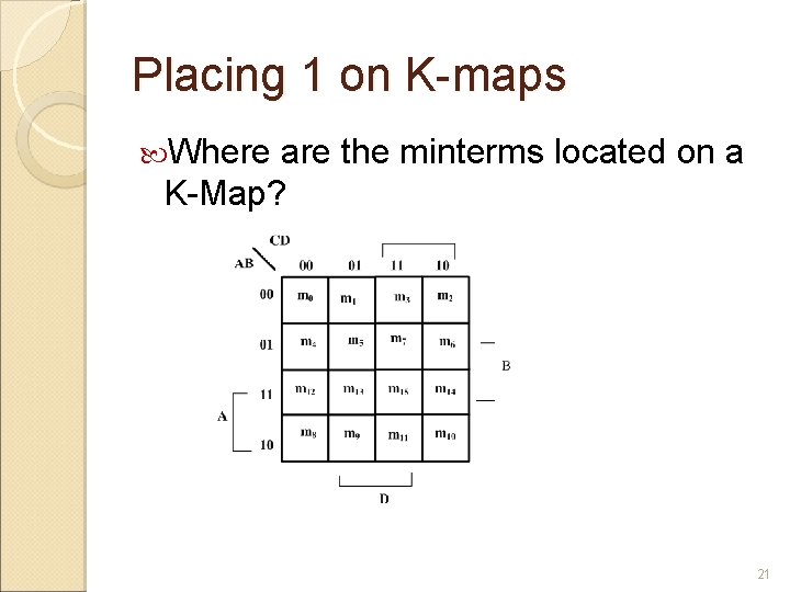
Placing 1 on K-maps Where are the minterms located on a K-Map? 21
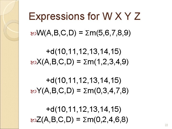
Expressions for W X Y Z W(A, B, C, D) = Σm(5, 6, 7, 8, 9) +d(10, 11, 12, 13, 14, 15) X(A, B, C, D) = Σm(1, 2, 3, 4, 9) +d(10, 11, 12, 13, 14, 15) Y(A, B, C, D) = Σm(0, 3, 4, 7, 8) +d(10, 11, 12, 13, 14, 15) Z(A, B, C, D) = Σm(0, 2, 4, 6, 8) 22
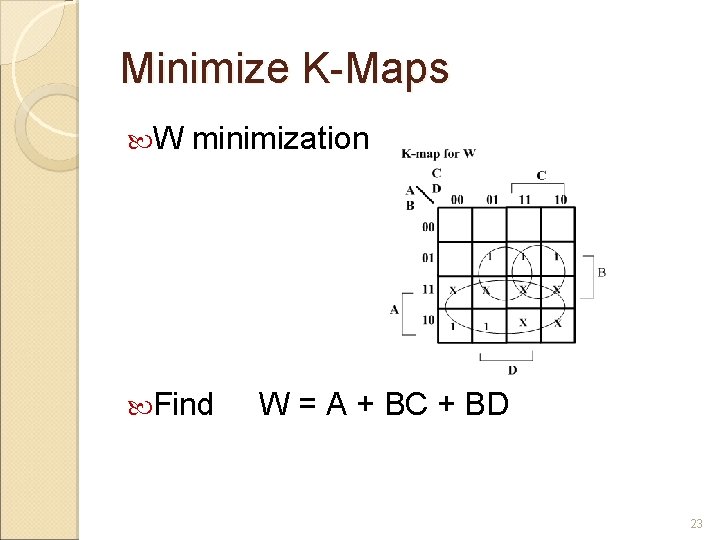
Minimize K-Maps W minimization Find W = A + BC + BD 23
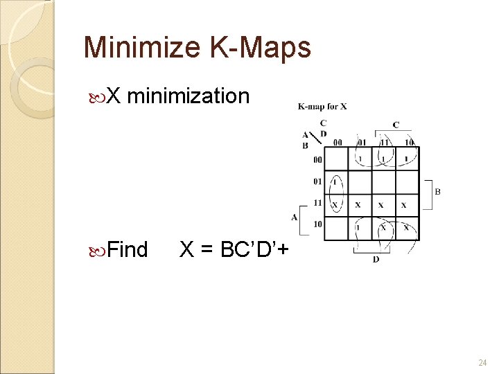
Minimize K-Maps X minimization Find X = BC’D’+B’C+B’D 24
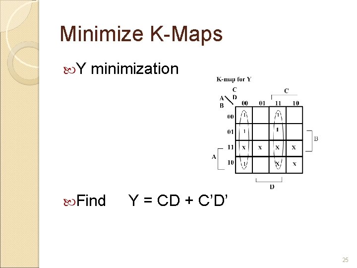
Minimize K-Maps Y minimization Find Y = CD + C’D’ 25
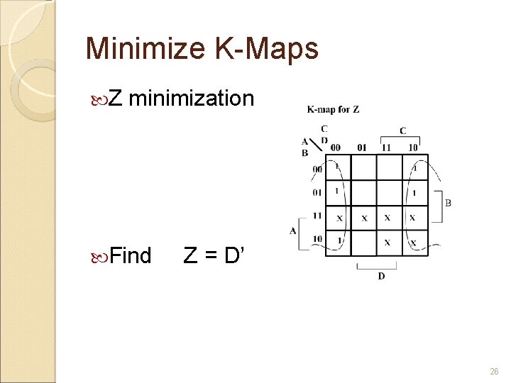
Minimize K-Maps Z minimization Find Z = D’ 26
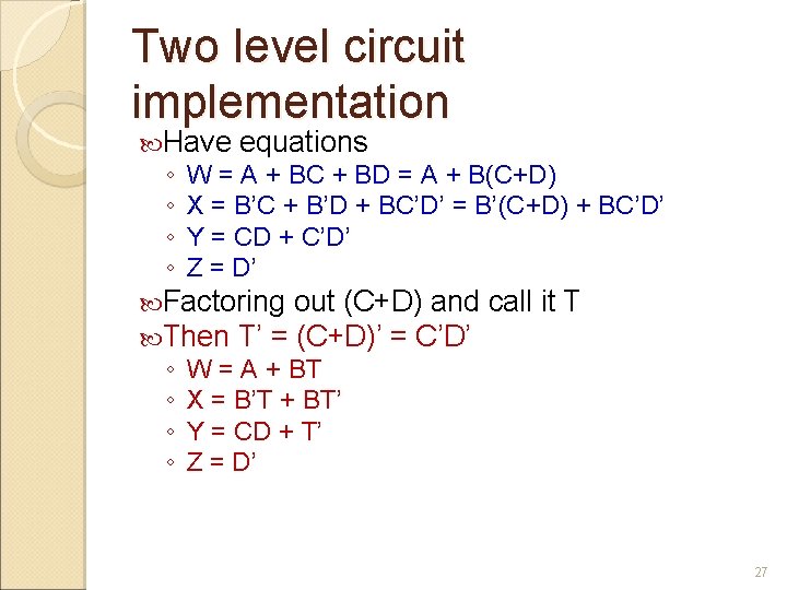
Two level circuit implementation Have ◦ ◦ equations W = A + BC + BD = A + B(C+D) X = B’C + B’D + BC’D’ = B’(C+D) + BC’D’ Y = CD + C’D’ Z = D’ Factoring out (C+D) and Then T’ = (C+D)’ = C’D’ ◦ ◦ call it T W = A + BT X = B’T + BT’ Y = CD + T’ Z = D’ 27
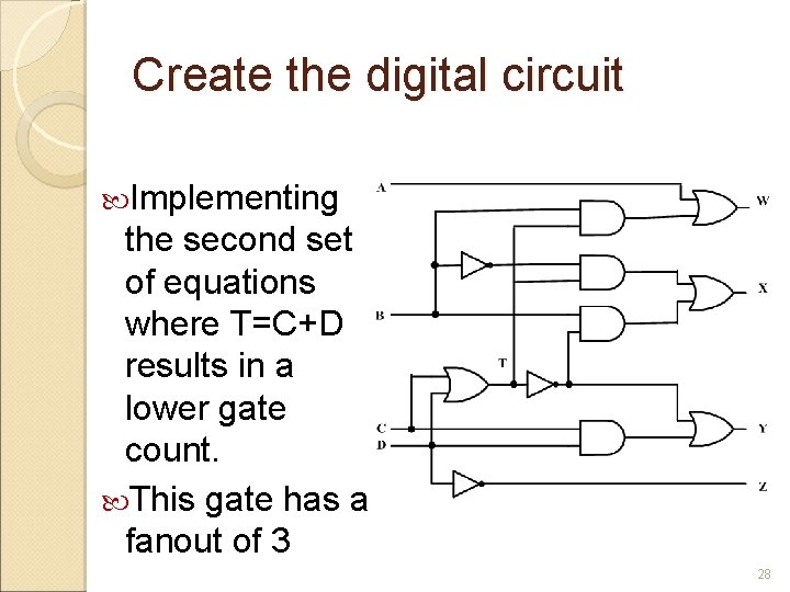
Create the digital circuit Implementing the second set of equations where T=C+D results in a lower gate count. This gate has a fanout of 3 28
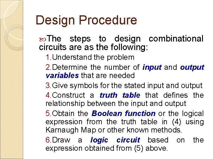
Design Procedure The steps to design combinational circuits are as the following: 1. Understand the problem 2. Determine the number of input and output variables that are needed 3. Give symbols for the stated input and output 4. Construct a truth table that defines the relationship between the input and output 5. Obtain the Boolean function or the logical expression from the truth table in (4) using Karnaugh Map or other known methods. 6. Draw a logic circuit based on the expression obtained from (5) above.
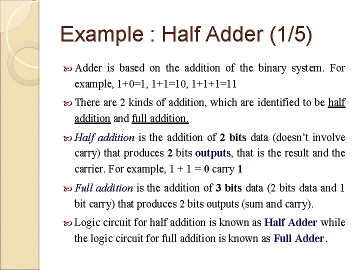
Example : Half Adder (1/5) Adder is based on the addition of the binary system. For example, 1+0=1, 1+1=10, 1+1+1=11 There are 2 kinds of addition, which are identified to be half addition and full addition. Half addition is the addition of 2 bits data (doesn’t involve carry) that produces 2 bits outputs, that is the result and the carrier. For example, 1 + 1 = 0 carry 1 Full addition is the addition of 3 bits data (2 bits data and 1 bit carry) that produces 2 bits outputs (sum and carry). Logic circuit for half addition is known as Half Adder while the logic circuit for full addition is known as Full Adder.
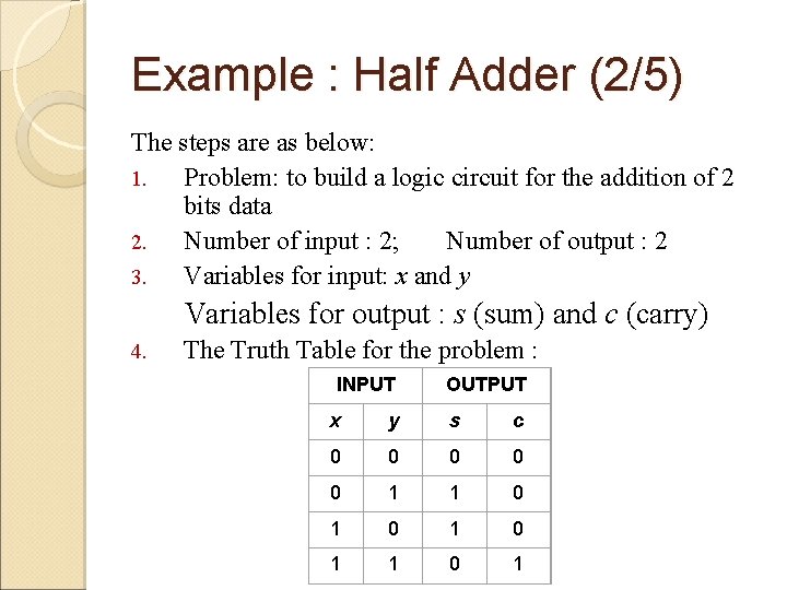
Example : Half Adder (2/5) The steps are as below: 1. Problem: to build a logic circuit for the addition of 2 bits data 2. Number of input : 2; Number of output : 2 3. Variables for input: x and y Variables for output : s (sum) and c (carry) 4. The Truth Table for the problem : INPUT OUTPUT x y s c 0 0 0 1 1 0 1 0 1
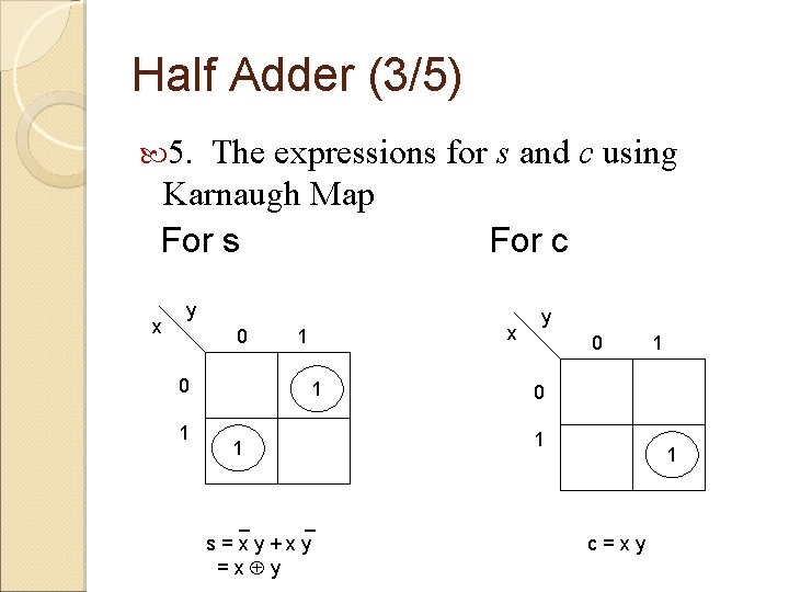
Half Adder (3/5) 5. The expressions for s and c using Karnaugh Map For s For c x y 0 0 1 x 1 1 1 _ _ s=xy+xy =x y y 0 1 1 c=xy
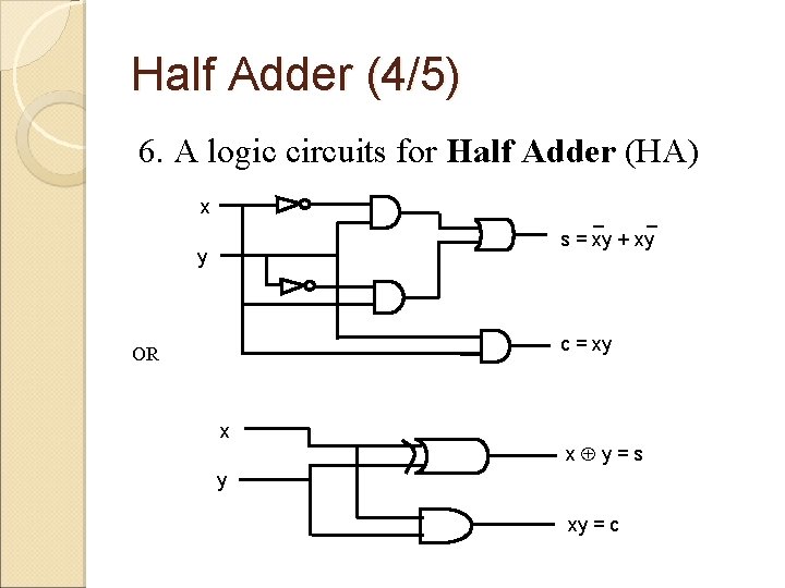
Half Adder (4/5) 6. A logic circuits for Half Adder (HA) x _ _ s = xy + xy y c = xy OR x x y=s y xy = c
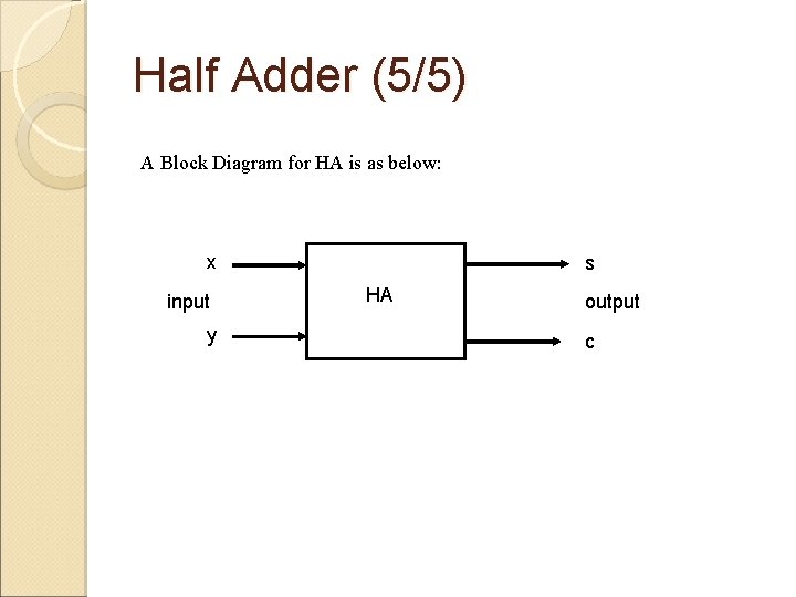
Half Adder (5/5) A Block Diagram for HA is as below: x input y s HA output c
Designing a Circuit for Full Adder (FA) The same method used to design HA. Problem: Build logic circuit for the addition of 3 bits data Number of input : 3 Number of output : 2 Variables for input: x , y and ci Variables for output : s (sum) and co (carry)
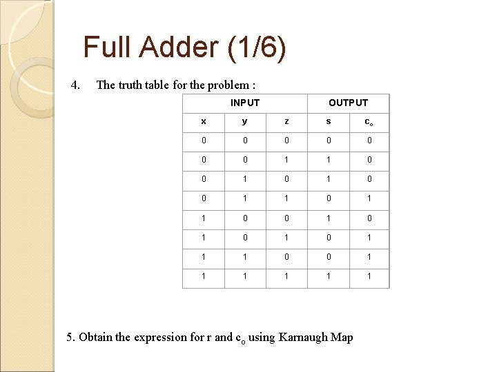
Full Adder (1/6) 4. The truth table for the problem : INPUT OUTPUT x y z s co 0 0 0 0 1 1 0 0 1 0 1 1 1 0 0 1 1 1 5. Obtain the expression for r and co using Karnaugh Map
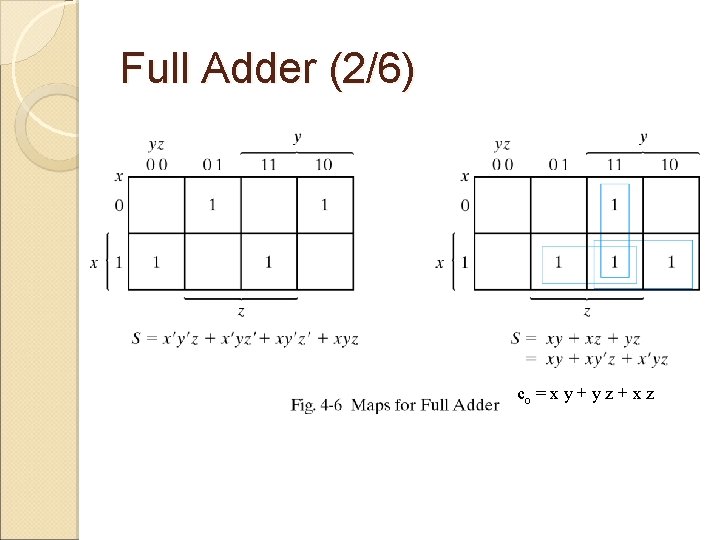
Full Adder (2/6) co = x y + y z + x z
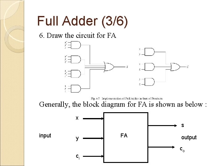
Full Adder (3/6) 6. Draw the circuit for FA Generally, the block diagram for FA is shown as below : x s input y ci FA output co
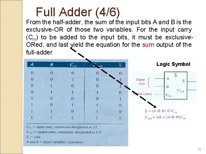
Full Adder (4/6) From the half-adder, the sum of the input bits A and B is the exclusive-OR of those two variables. For the input carry (Cin) to be added to the input bits, it must be exclusive. ORed, and last yield the equation for the sum output of the full-adder Logic Symbol 39
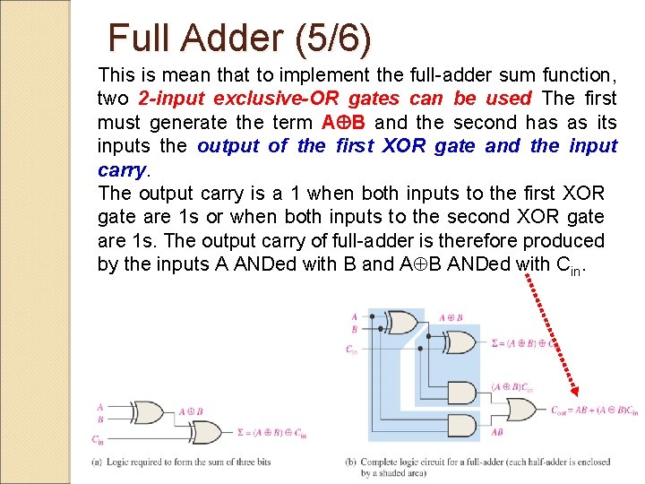
Full Adder (5/6) This is mean that to implement the full-adder sum function, two 2 -input exclusive-OR gates can be used The first must generate the term A B and the second has as its inputs the output of the first XOR gate and the input carry. The output carry is a 1 when both inputs to the first XOR gate are 1 s or when both inputs to the second XOR gate are 1 s. The output carry of full-adder is therefore produced by the inputs A ANDed with B and A B ANDed with Cin. 40
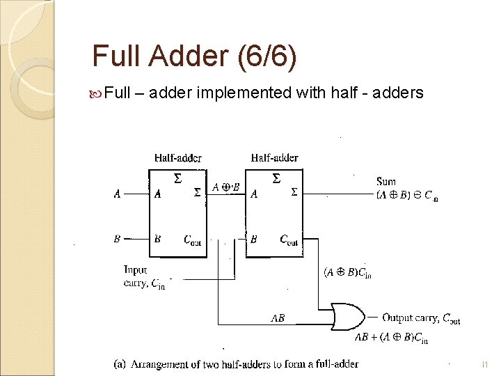
Full Adder (6/6) Full – adder implemented with half - adders 41
Binary Adders - Introduction Question: ◦ How do you design a adder circuit when you have more than 3 binary inputs? Solution: Binary adder that produces the arithmetic sum of binary numbers can be constructed with full adders connected in cascade. Here, the output carry from each full adder connected to the input carry of the next full adder in the chain. Note that the input carry C 0 in the least significant position must be 0.
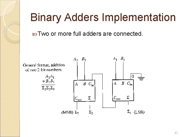
Binary Adders Implementation Two or more full adders are connected. 43
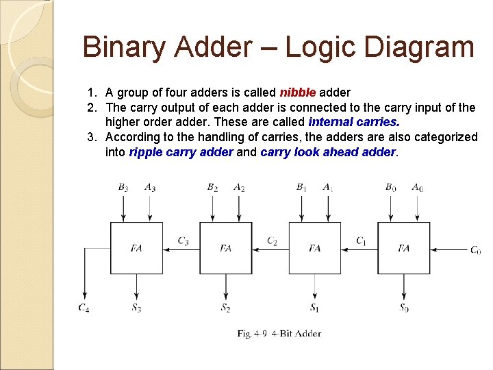
Binary Adder – Logic Diagram 1. A group of four adders is called nibble adder 2. The carry output of each adder is connected to the carry input of the higher order adder. These are called internal carries. 3. According to the handling of carries, the adders are also categorized into ripple carry adder and carry look ahead adder.
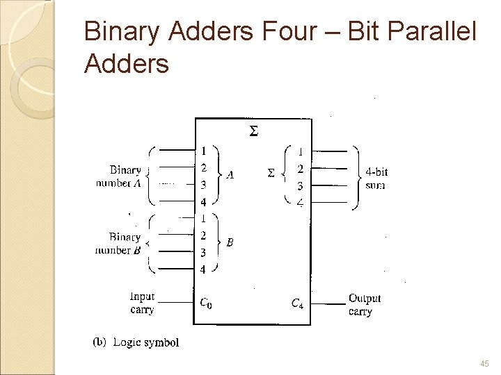
Binary Adders Four – Bit Parallel Adders 45
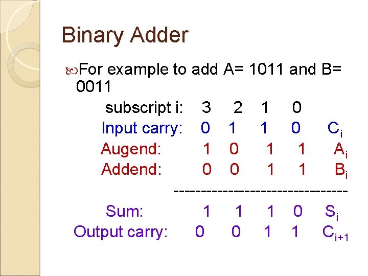
Binary Adder For example to add A= 1011 and B= 0011 subscript i: 3 2 1 0 Input carry: 0 1 1 0 Ci Augend: 1 0 1 1 Ai Addend: 0 0 1 1 Bi ----------------Sum: 1 1 1 0 Si Output carry: 0 0 1 1 Ci+1
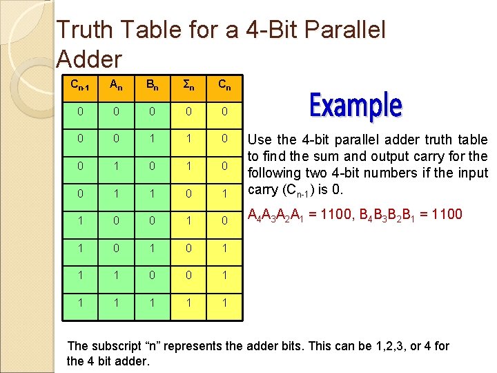
Truth Table for a 4 -Bit Parallel Adder Cn-1 An Bn Σn Cn 0 0 0 0 1 1 0 0 1 1 0 1 Use the 4 -bit parallel adder truth table to find the sum and output carry for the following two 4 -bit numbers if the input carry (Cn-1) is 0. 1 0 0 1 0 A 4 A 3 A 2 A 1 = 1100, B 4 B 3 B 2 B 1 = 1100 1 0 1 1 1 0 0 1 1 1 The subscript “n” represents the adder bits. This can be 1, 2, 3, or 4 for the 4 bit adder.
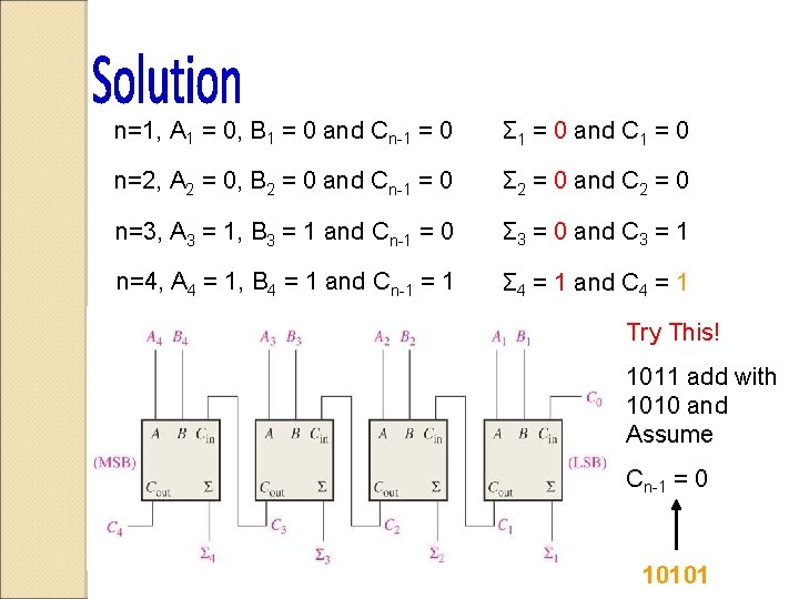
n=1, A 1 = 0, B 1 = 0 and Cn-1 = 0 Σ 1 = 0 and C 1 = 0 n=2, A 2 = 0, B 2 = 0 and Cn-1 = 0 Σ 2 = 0 and C 2 = 0 n=3, A 3 = 1, B 3 = 1 and Cn-1 = 0 Σ 3 = 0 and C 3 = 1 n=4, A 4 = 1, B 4 = 1 and Cn-1 = 1 Σ 4 = 1 and C 4 = 1 Try This! 1011 add with 1010 and Assume Cn-1 = 0 10101
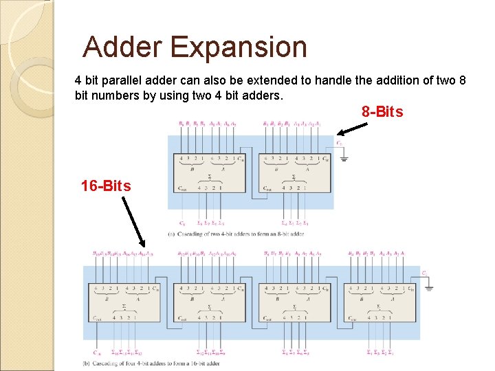
Adder Expansion 4 bit parallel adder can also be extended to handle the addition of two 8 bit numbers by using two 4 bit adders. 8 -Bits 16 -Bits
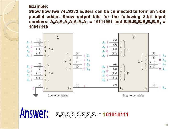
Example: Show two 74 LS 283 adders can be connected to form an 8 -bit parallel adder. Show output bits for the following 8 -bit input numbers: A 8 A 7 A 6 A 5 A 4 A 3 A 2 A 1 = 10111001 and B 8 B 7 B 6 B 5 B 4 B 3 B 2 B 1 = 10011110 Σ 8Σ 7Σ 6Σ 5Σ 4Σ 3Σ 2Σ 1 = 101010111 50
Home Work How do you develop a Binary Subtractor using combinational logic?
Comparators The basic function of a comparator is to compare the magnitude of two binary quantities to determine the relationship of those quantities. n n n 1 -Bit Comparator 2 -Bit Comparator 4 -Bit Comparator 52
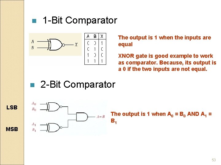
n 1 -Bit Comparator The output is 1 when the inputs are equal XNOR gate is good example to work as comparator. Because, its output is a 0 if the two inputs are not equal. n 2 -Bit Comparator LSB The output is 1 when A 0 = B 0 AND A 1 = B 1 MSB 53
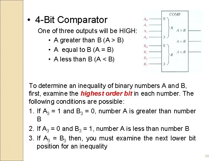
• 4 -Bit Comparator One of three outputs will be HIGH: • A greater than B (A > B) • A equal to B (A = B) • A less than B (A < B) To determine an inequality of binary numbers A and B, first, examine the highest order bit in each number. The following conditions are possible: 1. If A 3 = 1 and B 3 = 0, number A is greater than number B 2. If A 3 = 0 and B 3 = 1, number A is less than number B 3. If A 3 = B 3 then, you must examine the next lower bit position for an inequality 54
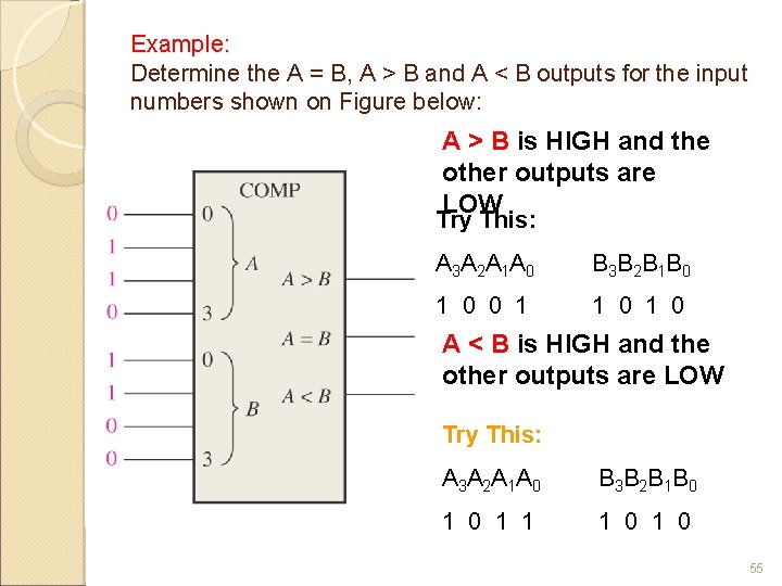
Example: Determine the A = B, A > B and A < B outputs for the input numbers shown on Figure below: A > B is HIGH and the other outputs are LOW Try This: A 3 A 2 A 1 A 0 B 3 B 2 B 1 B 0 1 0 0 1 1 0 A < B is HIGH and the other outputs are LOW Try This: A 3 A 2 A 1 A 0 B 3 B 2 B 1 B 0 1 1 1 0 55
Decoders Basic function of decoder is to detect the presence of a specified combinations of bits (code) on its inputs and to indicate the presence of that code by a specified output level. Its general form, a decoder has n input lines to handle n bits and from one to 2 n output line to indicate the presence of one or more n – bit combinations.
Basic Binary Decoder If you need to determine when a binary 1001 occurs on the input of a digital circuit. An AND gate can be used to produce HIGH when all the inputs are high. In order to make all the inputs are HIGH, we need two inverters for 2’nd and 3’rd bits. Therefore, 57
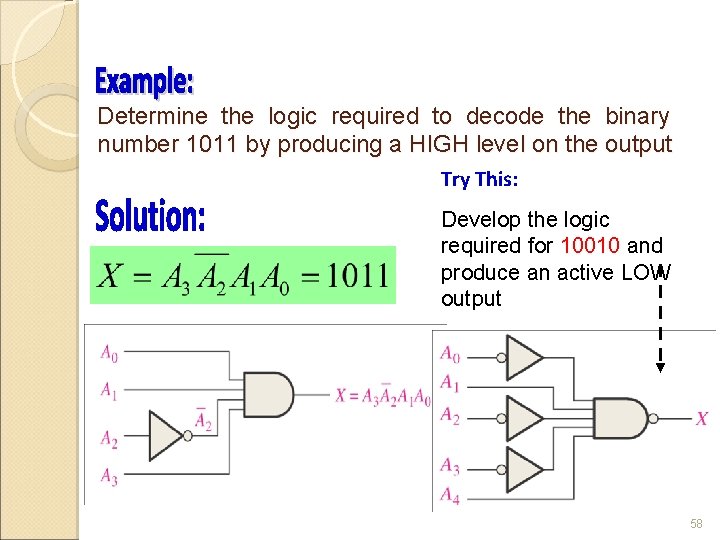
Determine the logic required to decode the binary number 1011 by producing a HIGH level on the output Try This: Develop the logic required for 10010 and produce an active LOW output 58
4 – Bit Decoder In order to decode all possible combinations of four bits, sixteen decoding gates are required (24 = 16). This decoder commonly called either a 4 – line – to – 16 – line decoder because there are four inputs and sixteen outputs. It can also be called 1 – of – 16 decoders because for any given code on the inputs, one of the sixteen outputs is activated. 59
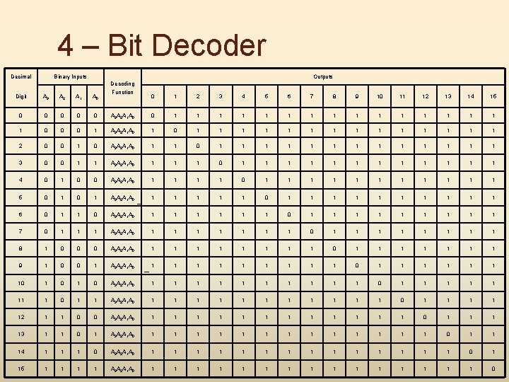
4 – Bit Decoder Decimal Binary Inputs Outputs Digit A 3 A 2 A 1 A 0 0 0 1 0 0 0 2 0 0 3 0 4 Decoding Function 0 1 2 3 4 5 6 7 8 9 10 11 12 13 14 15 A 3 A 2 A 1 A 0 0 1 1 1 1 A 3 A 2 A 1 A 0 1 1 1 1 1 1 1 1 0 1 1 A 3 A 2 A 1 A 0 1 1 1 1 0 0 A 3 A 2 A 1 A 0 1 1 1 1 5 0 1 A 3 A 2 A 1 A 0 1 1 1 1 6 0 1 1 0 A 3 A 2 A 1 A 0 1 1 1 1 1 7 0 1 1 1 A 3 A 2 A 1 A 0 1 1 1 1 8 1 0 0 0 A 3 A 2 A 1 A 0 1 1 1 1 9 1 0 0 1 A 3 A 2 A 1 A 0 1 1 1 1 1 0 1 1 1 10 1 0 A 3 A 2 A 1 A 0 1 1 1 1 1 0 1 1 11 1 0 1 1 A 3 A 2 A 1 A 0 1 1 1 0 1 1 12 1 1 0 0 A 3 A 2 A 1 A 0 1 1 1 0 1 13 1 1 0 1 A 3 A 2 A 1 A 0 1 1 1 1 0 1 1 14 1 1 1 0 A 3 A 2 A 1 A 0 1 1 1 1 0 1 15 1 1 A 3 A 2 A 1 A 0 1 1 1 1 0
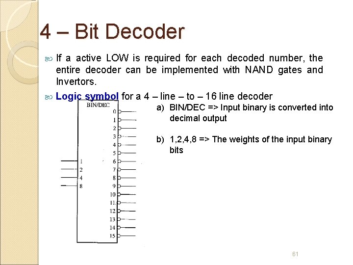
4 – Bit Decoder If a active LOW is required for each decoded number, the entire decoder can be implemented with NAND gates and Invertors. Logic symbol for a 4 – line – to – 16 line decoder a) BIN/DEC => Input binary is converted into decimal output b) 1, 2, 4, 8 => The weights of the input binary bits 61
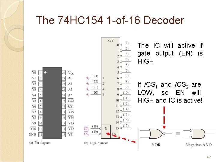
The 74 HC 154 1 -of-16 Decoder The IC will active if gate output (EN) is HIGH If /CS 1 and /CS 2 are LOW, so EN will HIGH and IC is active! 62
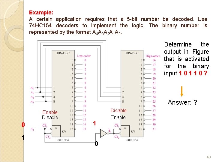
Example: A certain application requires that a 5 -bit number be decoded. Use 74 HC 154 decoders to implement the logic. The binary number is represented by the format A 4 A 3 A 2 A 1 A 0. Determine the output in Figure that is activated for the binary input 1 0 1 1 0 ? Answer: ? Enable Disable 0 1 1 Disable Enable 0 63
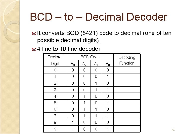
BCD – to – Decimal Decoder It converts BCD (8421) code to decimal (one of ten possible decimal digits). 4 line to 10 line decoder Decimal BCD Code Digit A 3 A 2 A 1 A 0 0 0 1 2 0 0 1 0 3 0 0 1 1 4 0 1 0 0 5 0 1 6 0 1 1 0 7 0 1 1 1 8 1 0 0 0 9 1 0 0 1 Decoding Function 64
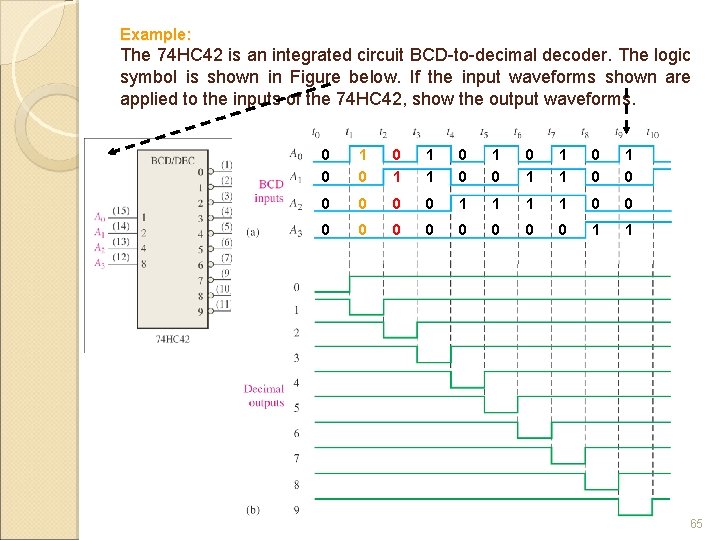
Example: The 74 HC 42 is an integrated circuit BCD-to-decimal decoder. The logic symbol is shown in Figure below. If the input waveforms shown are applied to the inputs of the 74 HC 42, show the output waveforms. 0 0 1 1 1 0 0 0 1 1 0 0 0 0 0 1 1 65
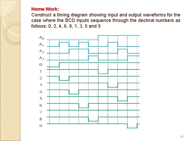
Home Work: Construct a timing diagram showing input and output waveforms for the case where the BCD inputs sequence through the decimal numbers as follows: 0, 2, 4, 6, 8, 1, 3, 5 and 9 66
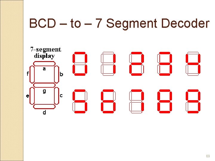
BCD – to – 7 Segment Decoder Accepts the BCD code on its inputs and provides outputs to drive 7 – segment display devices to produce a decimal readout. 67
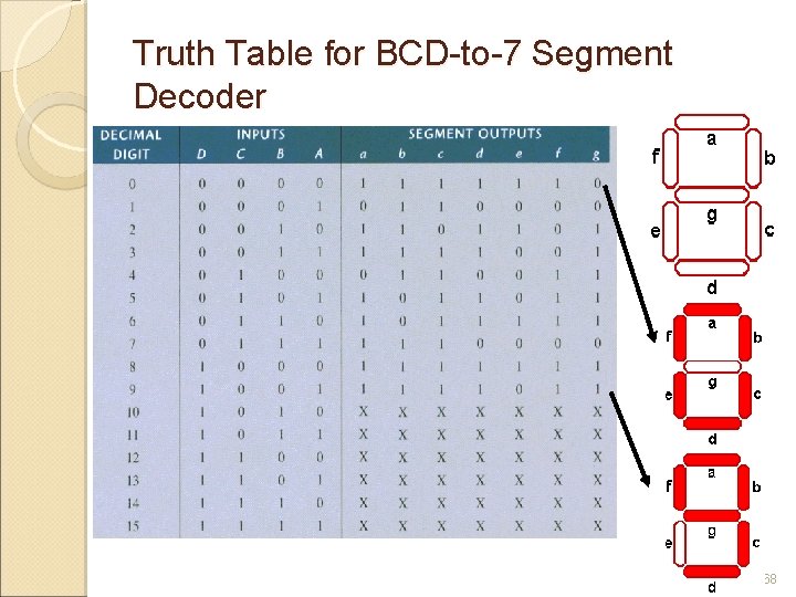
Truth Table for BCD-to-7 Segment Decoder 68
BCD – to – 7 Segment Decoder 69
Encoders Combinational logic circuit that essentially performs a “reverse” decoder function. Encoder accepts an active level on one of its input representing a digit, such as a decimal or octal digit, and convert it to a coded output, such as BCD or binary. Encoders can also be devised to encode various symbols and alphabetic characters. Process of converting from familiar symbols or numbers to a coded format is called coding. 70
Decimal – to – BCD Encoders Has 10 inputs – one for each decimal digit – and four outputs corresponding to the BCD code. This is a basic 10 – line – to – 4 – line encoder. 71
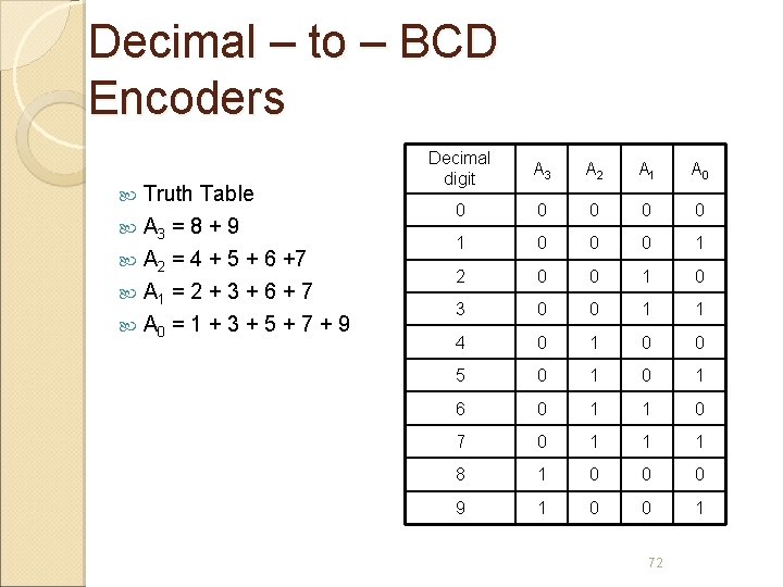
Decimal – to – BCD Encoders Truth Table A 3 = 8 + 9 A 2 = 4 + 5 + 6 +7 A 1 = 2 + 3 + 6 + 7 A 0 = 1 + 3 + 5 + 7 + 9 Decimal digit A 3 A 2 A 1 A 0 0 0 1 2 0 0 1 0 3 0 0 1 1 4 0 1 0 0 5 0 1 6 0 1 1 0 7 0 1 1 1 8 1 0 0 0 9 1 0 0 1 72
Decimal – to – BCD Encoders Basic logic diagram 73
Decimal – to – BCD Encoders Priority Encoder will produce a BCD output corresponding to the highest – order decimal digit input that is active and will ignore any other lower – order active inputs. Example : If 6 and 3 inputs are both active, BCD output is 0110 (represent decimal number 6). 74
8 – Line – to – 3 – Line Encoder 75
Code Converters Methods of using combinational logic circuits to convert from one code to another. 76
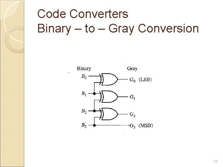
Code Converters Binary – to – Gray Conversion 77
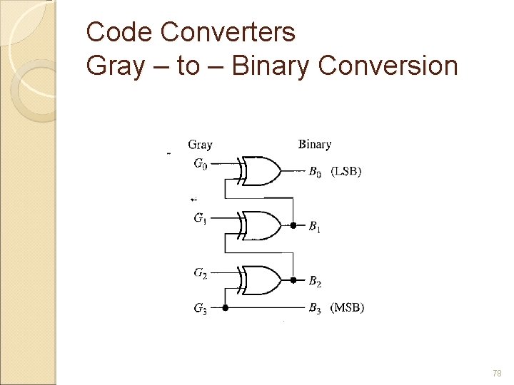
Code Converters Gray – to – Binary Conversion 78
Multiplexers A device that allows a digital information from several sources to be routed onto a single line for transmission over that line to a common destination. Basic multiplexer has several data – input lines and a single output line. It also has data – select inputs, which permit digital data on any one of the inputs to be switched to the output line. Also known as data selectors. 79
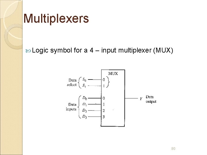
Multiplexers Logic symbol for a 4 – input multiplexer (MUX) 80
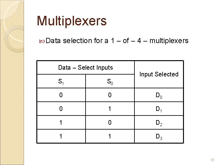
Multiplexers Data selection for a 1 – of – 4 – multiplexers Data – Select Inputs Input Selected S 1 S 0 0 0 D 0 0 1 D 1 1 0 D 2 1 1 D 3 81
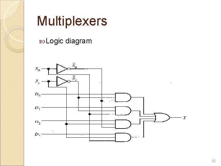
Multiplexers Logic diagram 82
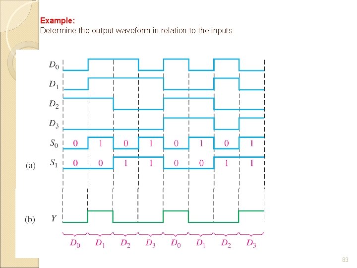
Example: Determine the output waveform in relation to the inputs 83
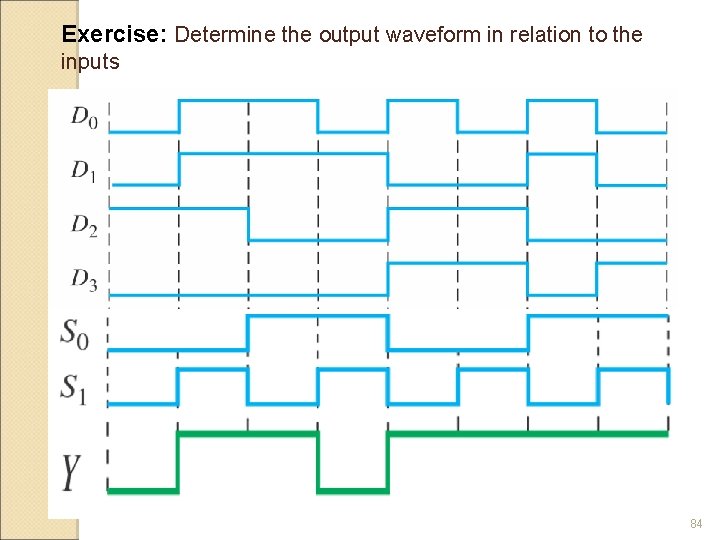
Exercise: Determine the output waveform in relation to the inputs 84
Demultiplexers Reverse the multiplexing function. It takes digital line and distributes it to a given number of output lines. Also known as data distributor. 85
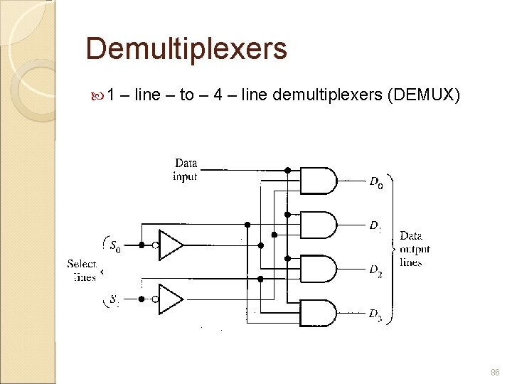
Demultiplexers 1 – line – to – 4 – line demultiplexers (DEMUX) 86
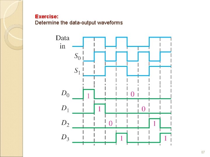
Exercise: Determine the data-output waveforms 87
Parity Generators / Checkers Errors can occur as digital codes are being transferred from one point to another within a digital system or while codes are being transmitted from one system to another. Errors can take form of undesired changes in the bits (1 change to 0 or vice versa). Parity method of error detection is when a parity bit is attached to a group of information bits in order to make the total number of 1 s either even or odd (depending on the system) 88
Basic Parity Logic In order to check for or to generate the proper parity in a given code, a basic principle can be used : The sum (disregarding carriers) of an even number of 1 s is always 0, and the sum of an odd number of 1 s is always 1. To determine if a given code has even parity or odd parity, all the bits in that code are summed. 89
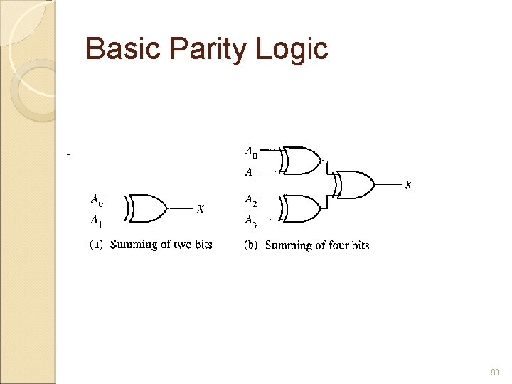
Basic Parity Logic 90
Parity Checker When the device is used as an even parity checker, the number of input bits should always be even; and when parity error occurs, the Even output goes LOW and the Odd output goes HIGH. When it used as odd parity checker, the number of input bits should always be odd; and when parity error occurs, the Odd output goes LOW and the Even output goes HIGH. 91
Parity Generator Even parity generator The parity bit is taken at the Odd output because this output is: 0 if there is an even number of input bits 1 if there is an odd number. Odd parity generator The parity bit is taken at the Even output because this output is: 0 if there is an odd number of input bits 1 if there is an even number. 92
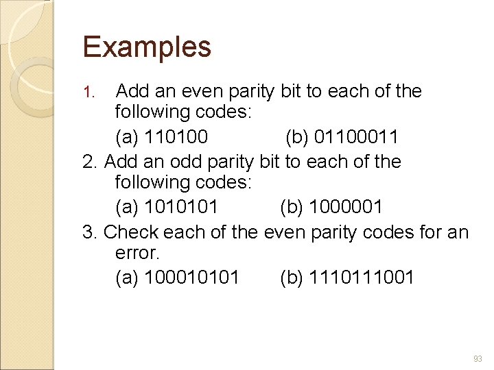
Examples Add an even parity bit to each of the following codes: (a) 110100 (b) 01100011 2. Add an odd parity bit to each of the following codes: (a) 1010101 (b) 1000001 3. Check each of the even parity codes for an error. (a) 100010101 (b) 111001 1. 93
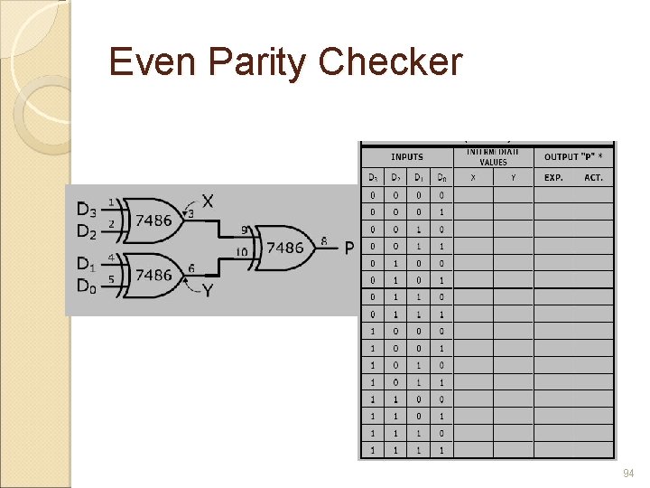
Even Parity Checker 94
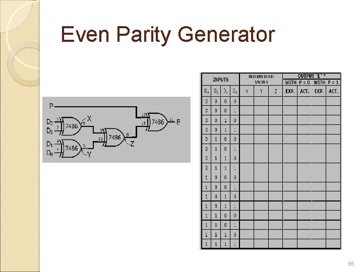
Even Parity Generator 95
Exercises Homework: Odd Parity Checker and Odd Parity Generator. 96

THANK YOU END OF CHAPTER 4
- Slides: 97